Abstract
Tip-enhanced near-field optical microscopy (TENOM) is a scanning probe technique capable of providing a broad range of spectroscopic information on single objects and structured surfaces at nanometer spatial resolution and with highest detection sensitivity. In this review, we first illustrate the physical principle of TENOM that utilizes the antenna function of a sharp probe to efficiently couple light to excitations on nanometer length scales. We then discuss the antenna-induced enhancement of different optical sample responses including Raman scattering, fluorescence, generation of photocurrent and electroluminescence. Different experimental realizations are presented and several recent examples that demonstrate the capabilities of the technique are reviewed.
1 Introduction
Since the first reports about 15 years ago tip-enhanced near-field optical microscopy (TENOM) has continuously developed and is now a powerful and versatile technique capable of producing high-spatial resolution optical images combined with strong signal enhancement. This development has been followed by a number of review articles.1-6 In this review we briefly illustrate the physical principle of TENOM and describe the different experimental realizations. We focus on more recent progress within the last five years both with respect to our conceptual understanding of tip-enhancement and regarding experimental improvements.
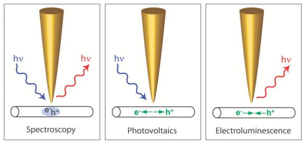
Conceptually the development of a clear description of the antenna function of the tip that is the origin of signal enhancement was an important step leading to the introduction of the term optical antenna and the definition of its key parameters.7-9 Following this concept tips can enhance several distinct photophysical sample responses including photo-induced light emission, photovoltaic responses and electrically driven light emission (Fig. 1).7
Fig. 1.
Optical antennas formed by metal nanostructures efficiently convert propagating radiation into localized energy in a nearby object. Conversely, localized energy is coupled to propagating radiation. Applications of antenna enhancement: (a) optical spectroscopy, (b) photovoltaics and (c) electroluminescence (adapted with permission from ref. 7. Copyright OSA 2009).
Experimental improvements have been achieved mainly regarding new probe designs often stimulated by antenna structures used in the radio and microwave frequency range. Moreover, the development of new probes was substantially supported by refined modeling of their enhancement characteristics and facilitated by our improving capabilities regarding nanofabrication. Besides being tailored towards optimum signal enhancement antenna structures were also designed to open up new illumination and detection schemes.
We then review several recent examples of TENOM applications with the focus on single molecule and single nanoobject experiments to illustrate the capabilities of the technique. In contrast to high-resolution far-field schemes such as photo-activated localization microscopy (PALM), stochastic optical reconstruction microscopy (STORM) and stimulated emission depletion microscopy (STED) that are limited to date to fluorescent samples, tip-enhancement turned out to be a more general and versatile scheme. TENOM is shown to be applicable to various types of signals including Raman scattering and fluorescence as well as photocurrent and electroluminescence. In addition, the enhanced detection sensitivity of TENOM makes it ideally suited to study very weak responses resulting from single molecules or single nanoobjects.
2 Physical background
2.1 Diffraction, optical near-field/far-field
The diffraction limit of conventional optical microscopy is the result of limited spatial frequencies being carried by propagating optical fields from the sample to the detector. This can be visualized for example using the angular spectrum representation of optical fields10 in which free-space propagation of spectral field components (kx, ky, z = 0) into the z-direction can be calculated by multiplication with the propagator exp(ikzz). The wave vector component is given by the wavelength of light λ and the refractive index n. For small spatial frequencies (kx2 + ky2) < (2πn/λ)2 the z-component kz is real and the associated waves propagate along the z-direction. For larger spatial frequencies (kx2 + ky2) > (2πn/λ)2 the z-component kz is imaginary and the associated wave becomes evanescent.
We note that for optical detection after sample illumination the window of spatial frequencies (kx2 + ky2) can be shifted in k-space by structuring the illumination intensity (structured illumination microscopy, SIM). This can be used to extend the detected spatial frequency range and can provide a spatial resolution factor of 2 below the Abbe limit.
High-resolution near-field optical techniques exploit short-ranged sample–probe interactions mediated by evanescent fields. First near-field microscopy images of single fluorescent molecules have been reported using aperture probes that make use of the near-field interaction between a sub-wavelength aperture and the sample.11 Another approach utilizes active probes such as fluorescent molecules or defect centers in diamond. Here the near-field interaction with the sample, typically dipole–dipole based, is detected as a change in the optical properties of the probe (e.g. ref. 12-14).
In tip-enhanced near-field optical microscopy the evanescent near-field in the vicinity of sharp metallic probes is used to interact with the sample. Crucially, the antenna function of the probe provides efficient coupling between the far-field and the probe’s near-field. As a result signal enhancement for objects in the vicinity of the probe can be achieved using a laser source and a detector in the far-field. This signal enhancement and the correspondingly improved detection sensitivity are essential since high spatial resolution is connected to a shrinking sample volume and weaker signals.
2.2 Optical antennas
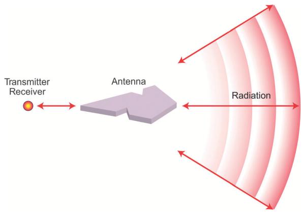
In tip-enhanced near-field optical microscopy the tip acts as an optical antenna by efficiently converting free propagating radiation into localized energy and vice versa.7-9,15 This localized energy can be used to optically excite a receiving object that is in the near-field of the antenna’s feed point leading to enhanced absorption of radiation (Fig. 2). Conversely, energy released by a transmitting object can be radiated more efficiently. The analogy to radio frequency and microwave antennas stimulated the adoption of their well-developed concepts and of the corresponding formalism and terminology.
Fig. 2.
Transmitting/receiving antenna. Arrows indicate the direction of energy flow. The two configurations are related by the principle of reciprocity. In spectroscopy and microscopy, the two antenna concepts are combined; that is, the antenna is used both as a receiver and as a transmitter (Figure adapted with permission from ref. 9, ©2011 NPG.).
Enhanced absorption can be discussed in terms of the antenna aperture A(θ, φ, npol) = Pexc/I(θ, φ) that describes the efficiency with which the radiation of intensity I and polarization npol incident from the direction (θ, φ) is captured by the antenna to excite the receiver with power Pexc. Formally, the antenna aperture corresponds to the absorption cross section of the receiver in the presence of the antenna σ = A.7 Assuming a dipole-like receiver oriented along np with cross section σ0 without antenna, σ can be expressed in terms of the local fields E and E0 with and without antenna as
| (1) |
Neglecting their vectorial character or assuming the same direction of enhanced and non-enhanced fields, the absorption enhancement can then be expressed by the local field enhancement factor f = E/E0 as σ/σ0 = f2. On the other hand, eqn (1) clearly illustrates that the absorption enhancement provided by an antenna in general depends on the direction and the polarization of the incident radiation. For metallic antennas particularly strong local fields can result in the optical regime from localized surface plasmon resonances, collective electron oscillations that are controlled by their shape and their material composition (see Section 3.1).
Enhanced spontaneous emission can be discussed in terms of the antenna efficiency εrad and the antenna gain G. While the efficiency measures the ratio between emitted power Prad and the total dissipated power P corresponding to εrad = Prad/P, the antenna gain also considers the angular distribution of the radiated power determined by the directivity D(θ, φ) following
| (2) |
Absorption and emission at the same optical frequency can be connected following the reciprocity theorem. For a dipolar absorber/emitter, reciprocity leads to a relationship between its excitation rate Γexc and its spontaneous emission rate Γrad.7,9
| (3) |
Here, the superscript “0” refers to the absence of the antenna and the subscript “θ” indicates the polarization state; that is, the electric field vector points in the direction of the θ unit vector. An equivalent equation holds for polarization in the φ direction. A good transmitting antenna is therefore also a good receiving antenna. Interestingly, excitation in a direction of high directivity allows the excitation rate to be enhanced more strongly than the radiative rate.7,9 Neglecting again the vectorial character or assuming the same direction of enhanced and non-enhanced fields, the spontaneous emission rate enhancement can also be expressed by the local field enhancement factor f = E/E0 as Γrad/ = f2.
Evidently, the angular dependence of the antenna aperture A and directivity D are of prime importance for the resulting signal enhancement and need to be considered in the design of the experiment and the optical microscope (Section 3.2). In addition, both antenna characteristics can exhibit a pronounced frequency dependence, e.g. in the case of plasmonic particle resonances of different multipolar orders (Section 2.3).
Several important differences between optical antennas based on metals and their long-wavelength counterparts exist that are mostly due to the fact that metals are not perfect conductors at optical frequency. Key distinctions include intrinsic material resonances such as quantum state excitations (metals, semiconductor homo- and heterostructures) and extrinsic resonances (surface plasmon/phonon polaritons) at optical frequencies. Moreover, in the absence of discrete inductors, capacitors, and resistors, used in connection with RF antennas new design strategies must be developed to impedance match the antenna to the load, ultimately in the form of a vibrational, electronic, or spin excitation on the quantum level.15
2.3 Signal enhancement
As discussed in the previous section, it is the antenna function of a tip that enhances the optical response of the sample by increasing both the excitation and the spontaneous emission rate. In the experiment care has to be taken in order to match the excitation profile and the angular detection range of the optical microscope to the antenna aperture and directivity (Section 3.2). The following discussion shows how distinct optical processes can be enhanced using optical antennas.
2.3.1 Tip-enhanced Raman scattering (TERS)
In the case of Raman scattering the signal depends on the product of the transition rates Γexc, θ(θ, φ)Γrad, the directivity Dθ(θ, φ) and the detection efficiency ηθ(θ, φ) of the experimental setup. Furthermore all these quantities will be wavelength dependent. The total signal at a given wavelength then results from angular integration
| (4) |
The φ integration can be limited to the maximum collection/detection angle φm = arcsin(NA/n) determined by the numerical aperture NA of the microscope objective and the refractive index n of the enclosing medium.
Antenna-enhanced Raman and fluorescence spectra can differ substantially from their far-field counterpart. In both cases the emission spectrum reflects the spectrally varying spontaneous emission rates Γrad connecting the same initial (virtual) state to different final states. Following the discussion in Section 2.2 and noting the frequency dependence of the antenna gain G in eqn (2) the antenna can thus substantially modify the spectral shape of emission. In the case of sharp antenna resonances and emission with large spectral bandwidth this will become particularly relevant.
Often, the angular and polarization dependence in eqn (4) is neglected together with the vectorial character of the electric fields (eqn (1)). As a consequence the total signal enhancement is found to scale approximately with the fourth power of the field enhancement for small differences between the excitation and emission wavelength and assuming that the field enhancement at the tip does not depend sensitively on the wavelength.
| (5) |
For the general case of surfaced enhanced Raman scattering (SERS), Raman enhancement factors are reported reaching up to 12 orders of magnitude for colloidal particle aggregates, rough metal films and particular multiple particle configurations involving interstitial sites between particles or outside sharp surface protrusions.16-18 Since the signal scales approximately with the fourth power, already moderate local field enhancement, predicted for a single spherical particle to be in the range of f ≈ 2–5 depending on its size and composition,10,17 is sufficient for significant signal enhancement.
Recent experimental reports of TERS investigations with sub-nanometer resolution that revealed the inner structure of single phorphyrin molecules on the silver surface point to an additional signal enhancement mechanism that occurs for very small tip-sample distances that depend very sensitively on the spectral resonance profile of the tip-surface system.19 Remarkably, this Raman signal featured a non-linear dependence on the laser intensity suggesting the occurrence of stimulated Raman scattering.
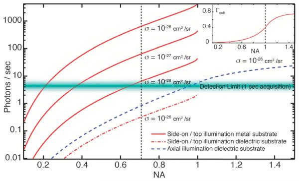
A semiquantitative analysis of the signal levels that can be expected in TERS from different sample materials and in different experimental geometries was performed by Berweger and Raschke.20 The authors discuss how high a signal level can actually be expected within the physical limitations set by field enhancement, damage threshold, tip scattering efficiency, collection and detection efficiency, and the Raman scattering cross section of the sample material for different experimental configurations (see Section 3.2 and Fig. 7).
Fig. 7.
Number of detected photons on a detector pixel as a function of the objective NA. Red curves are in a side-on/top illumination geometry with and without the use of a metallic substrate as indicated. With the dielectric substrate, we assume a Raman enhancement of ≈105. The dashed line indicates the maximum NA achievable in side-on illumination without the use of a parabolic mirror. The blue curve is under axial illumination (nsubstrate = noil = 1.5). The collection efficiency (inset) of the oil-immersion lens under axial illumination is based on results from ref. 106. The increased emission of light into the denser medium at angles greater than the critical angle is highly beneficial to TERS measurements. Thick green line represents the detection limit for 1 s acquisition time. It can be seen that side illumination benefits significantly from the increased field enhancement that arises due to plasmonic coupling to the metallic substrate. In contrast, the emission pattern of an emitter placed on a dielectric substrate significantly increases collection efficiency in an axial geometry when using oil-immersion objectives (Reprinted with permission from ref. 20. Copyright 2010 Elsevier.).
2.3.2 Tip-enhanced fluorescence
The fluorescence intensity depends on the excitation rate Γexc and the quantum yield q denoting the fraction of transitions from the excited state to the ground state that give rise to an emitted photon. The quantum yield is expressed in terms of the radiative rate Γrad and the non-radiative rate Γnon-rad through q = Γrad/(Γrad + Γnon-rad). Accordingly, the fluorescence enhancement due to the presence of the metal tip can be written as
| (6) |
As in the discussion of the Raman scattering signal in eqn (4) this simplified form neglects the orientation and polarization dependence of the transition rates and of the detection sensitivity together with the vectorial character of the electric field (eqn (1)).
From eqn (6) it is clear that TENOM works most efficiently for samples with small intrinsic fluorescence quantum yield q0 such as e.g. semiconducting single-walled carbon nanotubes and fullerenes.21-23 For a very low quantum yield emitter (q0 ≪ 1) the radiative rate can be neglected compared to the non-radiative rate. The quantum yield can then be approximated by q = Γrad/Γnon-rad. If the influence of the antenna on the non-radiative rate is small, the fluorescence enhancement is expected to scale with MFlu ≈ f4 as in the case of Raman scattering. For highly fluorescent samples, such as dye molecules, on the other hand, the quantum yield q0 is already close to unity and cannot be enhanced further. In this case fluorescence enhancement will only reflect the excitation rate enhancement MFlu ≤ Γexc/.
Because of the small separation between the emitter and the metal tip required for high spatial resolution (below 10 nm in typical experiments) non-radiative transfer of energy from the electronically excited molecule to the metal followed by non-radiative dissipation in the metal has to be taken into account. This process represents an additional non-radiative relaxation channel and reduces the number of detected fluorescence photons. While the theory of energy transfer between molecules and flat metal interfaces is well understood in the framework of phenomenological classical theory,24,25 nanometer sized objects are more difficult to quantify. Tip- and particle-induced radiative rate enhancement and quenching has been studied in the literature theoretically.26-32 Experiments on model systems formed by single dipole emitters such as molecules and semiconductor nanocrystals and spherical metal particles revealed a distance dependent interplay between competing enhancement and quenching processes.33-39 Here the role of emitter dipole orientation for the interplay between quenching and fluorescence enhancement becomes apparent.40 Small cone angles in tip-shaped metal structure are predicted to reduce energy dissipation as compared to spherical particles.30
Although semiconducting tips will cause less efficient quenching41,42 they will also provided weaker enhancement because of lower conductivity at optical frequencies. In addition, they do not support surface plasmon resonances.
While not directly observable in the experiment the change in the radiative rate can be extracted in principle from the measured excited state lifetime as the inverse of the sum of all decay rates τ−1 = Γrad + Γnon-rad and the measured intensity I. For a constant excitation rate with and without antenna, the radiative rate enhancement scales with the intensity ratio Γrad/ = I/I0. In most cases however, antenna-induced excitation rate modifications will complicate this analysis.
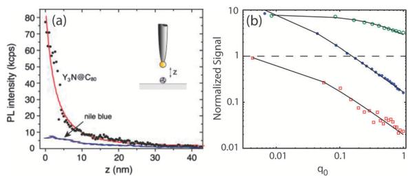
The influence of the intrinsic quantum yield q0 on the fluorescence enhancement was studied experimentally by several groups. Bharadwaj and Novotny23 realized the two limiting cases for high and low quantum yield emitters using nile blue and endohedral metallofullerene molecules. The antenna–molecule distance dependent measurements shown in Fig. 3(a) demonstrate stronger enhancement for the low quantum yield emitter and pronounced short-ranged quenching for the high quantum yield emitter as expected from the discussion made above.
Fig. 3.
(a) Fluorescence from a single endohedral metallofullerene molecule as a function of separation between the molecule and the gold nanoparticle. At short separations the nanoparticle antenna enhances the fluorescence by a factor of ≈100. For a single nile blue molecule the enhancement is in the range of 8–10. Dots are experimental data and the solid line is a fit according to a dipole model (Reprinted with permission from J. Phys. Chem. C, 2010, 114, 7444. Copyright 2010 American Chemical Society.). (b) Influence of the intrinsic quantum yield of a fluorescence emitter q0 on the detected signal intensity for gold coated (blue solid circles), silicon (green open circles) and CNT (red open circles) tips. The signal is normalized to the signal detected for large tip-sample distances. The dashed line separates enhancement and quenching (Reprinted with permission from E. Shafran, B. D. Mangum and J. M. Gerton, Phys. Rev. Lett., 107, 037403 (2011). Copyright (2011) by the American Physical Society.).
Shafran et al.43 investigated the influence of q0 on the signal enhancement for different tip materials by recording the dynamic fluctuations in quantum yield that occur during intensity blinking of single semiconductor nanocrystals (quantum dots). Intensity fluctuations were suppressed by efficient near-field coupling between the tip and emitter that causes rapid energy transfer to the tip. Tuning between tip-induced enhancement and quenching realized by a vertically oscillating tip made it possible to separate their contributions to the net fluorescence signal. These measurements showed that the near-field signal is dominated by enhancement for silicon tips, quenching for CNT tips, and can be tuned via q0 to either enhancement or quenching for gold-coated tips.
As discussed in Section 2.3.1 the spectral dependence of the antenna gain can lead to a significant modification of the shape of the emission spectrum. For a metal sphere antenna and single fluorescent molecules this has been demonstrated by Kühn et al.35
The influence of the antenna directivity and the resulting spatial redirection of emission has been studied for different antenna types including metal spheres, finite-length rod antennas and semi-infinite metal tips.35,44,45 These studies also highlighted the substantial influence of the dielectric substrate and the associated spatial emission distribution. Using back focal plane imaging of the photoluminescence (PL) emission excitation and emission rate enhancement could be distinguished and quantified for single semiconducting single-walled carbon nanotubes as was shown by Böhmler and co-workers.45
2.3.3 Photocurrent and electroluminescence
Photocurrent and electroluminescence spectroscopy provide insight into the optoelectronic properties of materials by probing correlated optical and charge carrier transport phenomena. Following the scheme in Fig. 1 the photovoltaic response is expected to benefit only from excitation rate enhancement and should thus scale with the square of the local field enhancement factor f2. Compared to the optical schemes discussed above this should lead to weaker enhancement and lower spatial resolution.
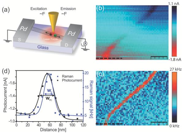
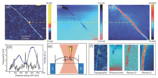
Fig. 4(b) and (c) show the simultaneously recorded antenna-enhanced Raman and zero-bias photocurrent signal of a single electrically contacted carbon nanotube. While the nanotube can be seen in both images with sub-diffraction resolution, the width of the photocurrent signal is apparently broader than that of the Raman signal. This can also be seen in the corresponding cross sections in Fig. 4(d). Both cross sections can be modeled using a Gaussian lineshape function using the peak width w as fitting parameter. Using the simplified scaling relation for the Raman signal enhancement in eqn (5) the Gaussian curve reflects the spatial dependence of the field enhancement factor f4(r). The photocurrent signal cross section should thus follow f2(r), the square root of the Raman signal cross section. The ratio of the Raman and photocurrent signal width is thus expected to be , very close to the experimentally determined ratio of 1.47. This supports the signal enhancement mechanism discussed above. Following the discussion of the signal enhancement of the photocurrent the electroluminescence should only benefit from emission rate enhancement.
Fig. 4.
Antenna-enhanced photocurrent microscopy. (a) Schematic of the experimental configuration using a carbon nanotube based device. (b) and (c) Simultaneously recorded zero-bias photocurrent and Raman scattering image, respectively. (d) Cross sections taken along the dashed lines in (b) and (c) together with fits using a Gaussian line shape function. The photocurrent signal features lower spatial resolution. The experimentally determined ratio of the Gaussian widths wPC/wR = 1.47 indicates that the photocurrent signal benefits only from excitation rate enhancement ∝f2 (Reprinted with permission from ACS Nano, 2012, 6, 6416. Copyright 2012 American Chemical Society.).
2.3.4 Quantification of near-field enhancement
Typical experimental configurations of tip-enhanced microscopy utilize far-field illumination of the tip antenna. As a result a far-field contribution without the tip is detected besides the signal resulting from the near-field interaction between the tip and the sample referred to as far-field background. The near-field to far-field background ratio depends on the probed volume and the dimensionality of the sample.46 For high-resolution imaging of surfaces the near-field signal results approximately from a circular sample surface area with a diameter dnf corresponding to the spatial resolution of π(dnf/2)2 whereas the confocal area is about π(λ/4)2 resulting in a surface area ratio of (λ/(2dnf))2. Considering bulk samples and taking into account the finite decay length of the near-field of about 10 nm and the longitudinal focal depth of about 500 nm in far-field microscopy, this ratio increases further by a factor of 50. From this discussion it is apparent that TENOM works most efficiently for spatially separated low dimensional structures such as quasi 1D quantum wires and nanotubes or quasi 0D emitters such as semiconductor nanocrystals and fluorescent molecules.
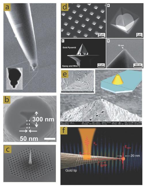
There are two possible strategies for increasing the near-field to far-field background ratio: the first is to increase the near-field signal by using antennas that show stronger field enhancement (see Section 3.1), the other is to reduce, suppress or separate the background contribution. This can be achieved by either using particular probes that avoid far-field excitation of the sample area (see Section 3.1 and Fig. 5(b, c, e and f)) or by separating the background by making use of the fact that the near-field signal decays rapidly with increasing tip-sample distance (see Section 3.2).
Fig. 5.
SEM images of different antenna structures. (a) Gold trimer antenna consisting of nanoparticles supported by a dielectric tip (Figure reproduced with permission from ref. 9, ©2011 NPG.). (b) Bowtie aperture antennas fabricated by FIB milling of an aluminum coated fiber probe (Reprinted with permission from Nano Lett., 2012, 12, 5972. Copyright 2012 American Chemical Society.). (c) Tapered plasmonic waveguide on top of a photonic crystal cavity for efficient photonic plasmonic coupling (Figure reproduced with permission from ref. 80, ©2010 NPG.). (d) Template-stripped 200 nm thick gold tips fabricated in anisotropically etched pyramidal molds on a Si wafer (Reprinted with permission from ACS Nano, 2012, 6, 9168. Copyright 2012 American Chemical Society.). (e) Coaxial antenna incorporated on the end of a scanning probe tip (Reprinted with permission from Nano Lett., 2011, 11, 1201. Copyright 2011 American Chemical Society.). (f) Etched gold wire tip with grating structure for SPP coupling and plasmonic nanofocusing (Reprinted with permission from J. Phys. Chem. Lett., 2012, 3, 945. Copyright 2012 American Chemical Society.).
The experimental quantification of the near-field enhancement and the local field enhancement factor based on a comparison of the detected intensity with and without antenna is difficult leading to a high degree of variability of the reported values even when the same tip material and excitation wavelength are used.5,47 There are several possible reasons for these discrepancies as discussed by Roy et al.47 Most of them can be attributed to the difficulties in separating the near-field from the far-field contribution and the quantification of the area or volume ratio mentioned above. For spatially isolated single quasi 0D emitters the latter is obsolete. In this case, however, the emitter has to be detectable also without signal enhancement or ensemble data need to be taken as reference. For sample materials of higher dimensionality, the unambiguous determination of the near-field enhancement taken into account the volume ratio is only possible for spatially uniform material properties.
Importantly, following the discussion in Section 2.2 the quantification of the near-field enhancement based on intensity data needs to consider the angular radiation pattern of the sample emitters, the antenna directivity, the angular and polarization dependent collection efficiency of the microscope setup and the orientations of the involved transition dipole moments. As an example the influence of the numerical aperture of the microscope and of the substrate material on the detectable Raman signal is shown below in Fig. 7 (see Section 3.2).
3 Experimental realization
3.1 Antenna types
There is a large variety of optical antenna designs that include different materials and shapes (see e.g. ref. 8, 9, and 48). Depending on the application one has to choose carefully the optimal design. Any optical antenna consists of a plasmonic nanostructure fabricated either with a top down technique such as electrochemical etching and focused ion-beam milling or with a bottom up technique as in colloidal chemistry.
Probably the most common near-field optical probes are solid metal tips made of gold or silver. Solid metal tips can be fabricated by electrochemical etching by dipping a metal wire into an etching solution and applying a voltage between the wire and a circular counter electrode immersed in the solution.49-51 In the case of gold tips the etching solution is fuming hydrochloric acid that can be mixed with ethanol resulting in tips with a radius of curvature that can be as low as 5 nm. While this technique delivers reproducibly sharp tips with a rather smooth surface, the actual geometrical shape given by the cone angle, the details of the surface structure and the exact diameter of the tip cannot be controlled. Together with the fact that the tips are not monocrystalline but consist of grains of different lattice configurations this is expected to lead to strongly varying field enhancement factors for selective tips.52,53 The latter problem could be solved using single crystalline gold nanostructures as both tip and substrate material.54,55 Moreover, spectral variations in the elastic scattering and photoluminescence spectra from tip to tip indicate the contribution of geometry-related particle-like surface plasmon resonances.56
In fact, the experimentally observed local field enhancement factors for electrochemically etched metal tips reported in the literature vary widely. Besides the geometrical factors mentioned above and the influence of the substrate discussed at the end of this section this can probably be attributed in part to variations in the tip-sample distance, the polarization and energy of the probed transitions and the efficiency of the signal collection realized in the experiment (see Sections 2.2 and 2.3.4). For electrochemically etched gold tips on glass field enhancement factors of f ≈ 5 have been derived from Raman studies on carbon nanotubes.47 Similar values can be derived from the excitation and emission rate enhancement observed in ref. 45. Experiments on gold tips in air using second harmonic generation (SHG) resulted in somewhat higher local field enhancement factors f ranging from 8–25.57 Recent studies of very smooth metal tips using electron scattering induced by fewcycle laser pulses to probe the near-field of the tips determined field enhancement factors f between 3 and 6.58 While the observed field enhancement clearly depended on the tip radius no significant differences were observed between gold and tungsten tips indicating that for these tip structures field enhancement results mainly from a geometrical lightning rod effect rather than from plasmonic or antenna resonances in agreement with theoretical modelling.58
An antenna probe with a more reproducible geometry that offers reliable enhancement factors is a single spherical metallic nanoparticle. The advantage of this probe is its simple geometry making a quantitative comparison between model calculations and experiment possible. This configuration has been experimentally realized using gold and silver particles attached to a glass tip as support by particle picking.34,35,59-62
For high quantum yield emitters and a particle diameter of 80 nm fluorescence enhancement factors of 13–15 and 8–9 at optimum antenna-molecule separation have been observed experimentally for silver and gold nanoparticles, respectively.7 Importantly, these enhancement factors are strongly frequency dependent reflecting the surface plasmon resonance of the particle and the competition between enhancement and metal-induced quenching.7,32,35,62
While in the quasi-static limit the near-field amplitude does not depend on the particle diameter, an interplay between size-dependent effects such as surface damping of electrons, radiative scattering and retardation leads to a maximum field enhancement at an excitation wavelength of 532 nm for gold particles with a diameter of about 50 nm.63 These antenna probes indeed deliver reproducible field enhancement factors in the experiment. However, for higher spatial resolution requiring very small nanoparticles, the strength of the enhanced fields cannot compete with that achievable with solid tips. Due to the larger particle diameter one has also to compromise on optical and topographic resolution. These disadvantages can be circumvented by optical antennas formed by two or more coupled metal nanoparticles of decreasing size.64 The realization of a trimer antenna consisting of three gold nanospheres with diameters of 80, 40 and 20 nm was presented by Novotny and co-workers (see Fig. 5(a)).9,65 In this geometry the enhanced field of the largest particle excites the next smaller one resulting in a field confinement given by the smallest particle at the end of the trimer. This cascade effect leads to a stronger fluorescence enhancement than would have been obtained with a single particle reaching a factor of about 40.65 Since the confinement is determined by the smallest particle, the optical and topographic resolution is superior compared to the single particle probe where a large diameter particle has to be used in order to achieve sufficient enhancement.
An in situ fabrication method of a near-field particle probe was presented by Sinjab et al.66 The authors used the laser of the optical setup to induce the controlled synthesis of silver nanoparticles at the tip apex that can be immediately used as a near-field probe. The advantage of this in situ method is the reduction of contamination and damage.
Johnson and co-workers67 introduced the fabrication of solid gold pyramidal tips by template stripping (see Fig. 5(d)). The power of this method is that it can be used for mass production and delivers uniform, sharp tips giving reproducible and strong local field enhancement of about 10. In addition, all tips have the same opening angle of 70.52° that is particularly well suited to scatter the near-field optical signal into the far-field.67
The most direct way for adding near-field functionality to an atomic force microscope (AFM) is to use metalized conventional AFM probes. Vapor-coating of the AFM tips with silver or gold under appropriate conditions leads to nanoparticle films that can provide very high enhancement factors.3,68,69 The reproducibility of the tip structure and the resulting polarization and directivity characteristics, however, is typically low.
The progress in nanoscale fabrication technologies enables more and more sophisticated and complex antenna designs often mimicking their counterpart in the radio frequency regime. Rod-shaped single particle antennas have been fabricated by different means. Here the aim is to exploit finite-length antenna resonances, for which their particular wavelength scaling behaviour needs to be considered.70 Taminiau et al.71 chose the length of a rod-shaped nanoantenna supported by a metal platform to match its -resonance. As a result the nanoantenna acted as an optical monopole. An alternative approach based on gold nanorods from colloidal synthesis was followed by Bharadwaj and co-workers.72
An example of two-particle structures are bowtie antennas that provide an intense local field between two facing nano-triangles.33,73-75 By focused ion beam milling, a bowtie antenna can be fabricated at the apex of a tapered optical fiber. Such a probe offers an excellent alternative to conventional fiber probes of similar opening area by increasing the power throughput through the fiber by three orders of magnitude (see Fig. 5(b)).76
Besides optimal enhancement some antenna designs aim at the elimination or reduction of the confocal background signal (Section 2.3.4). This can be achieved by avoiding direct exposure of the sample to the laser beam. In the so called tip-on-aperture approach this is done by illuminating the tip fabricated at the end of a metal-coated glass fiber with an evanescent wave resulting from a sub-wavelength aperture.77,78 High-spatial resolution and signal enhancement is provided by the sharp tip. In addition, tip fabrication allows tuning the tip length to match antenna resonances further maximizing field enhancement.71
Other schemes for avoiding the far-field background of the sample make use of plasmon propagation on the tip surface. Here, surface plasmon polaritons (SPPs) launched on the tip shaft at positions several micrometers away from the sample propagate towards the tip end creating a strong local field. The momentum mismatch between excitation light and propagating surface plasmons can be compensated by coupling the laser excitation to a grating structure written by FIB into the tip shaft (see Fig. 5(f)).15,79 Another realization of this scheme utilizes the near-field of a photonic crystal structure fabricated on the top part of the tip to funnel the excitation light into SPPs (see Fig. 5(c)).80 Efficient excitation of propagating plasmons can also be achieved using a higher order laser mode coupled into opaque metal coated tapered glass fibers.29,81,82 Bortchagovsky and co-workers83,84 introduced a probe design that does not require grating coupling or higher order laser modes for plasmon excitation. Here the probe is based on a tetrahedral glass fragment with an extremely sharp tip and edges (radius of curvature in the order of 3 nm) that is coated with a gold film of a thickness of 20–50 nm. The probe geometry supports a plasmon edge mode that can be remotely excited by a Gaussian laser beam incident onto the edge from within the transparent glass body of the tip analogous to the Kretschmann configuration for 2D surface plasmons on thin metal films.85
Leinhos et al.86 and Weber-Bargioni et al.87 suggested coaxial optical antennas that can be thought of as a metal–insulator–metal (MIM) slit. A strong enhancement is achieved by integrating a nanogap directly on the tip so that a metallic substrate as it is used in the gap-mode geometry is not required. These coaxial probes can be fabricated reproducibly with a high yield (see Fig. 5(e)). A similar design that employs a 3D tapered metal–insulator–metal structure ending in a nanogap is used for the so called campanile probe.88,89 Both probes based on a MIM structure offer a nearly background free imaging since the sample is illuminated by the confined field in the gap region only.
The field distribution and strength at the end of the tip is strongly dependent on the sample substrate. In a microscopic picture the oscillating charge distribution in the tip induces a mirror charge distribution in the substrate that can cause a further enhancement of the electric field strength. Apparently, the capability of the substrate material for supporting this image charge distribution, characterized by its dielectric function, determines the resulting field distribution and strength. Strongest local field enhancement thus results for metal substrates exceeding that for dielectric surfaces by orders of magnitude.90 Metal substrates are therefore ideal for Raman signal enhancement and TERS studies (see below Fig. 7).5,47 Due to metal-induced fluorescence quenching for short emitter-substrate separations an additional dielectric spacer layer would be needed for fluorescence studies reducing the achievable signal enhancement.
For emitters on an air–dielectric interface, e.g. fluorescent molecules on glass, the dielectric already leads to a significant modification of the spontaneous emission rate depending on the orientation of the molecule’s transition dipole moment.10 This can be exploited by optimized metal nanoparticle antenna configurations.91 Besides affecting the field strength and distribution, the spectral position of surface plasmon resonances in the tip will also shift upon decreasing tip-substrate distance depending on the dielectric functions of both materials.10,92,93
3.2 Microscopes
Since field enhancement is localized to the tip apex, schemes for tip-sample distance control working on the length scale of a few nanometers are required. Experimental implementations are based on normal or shear-force detection used in atomic force microscopy (AFM) or current detection as in scanning-tunneling microscopy (STM).94,95 Raster-scanning the probe thus yields both optical and topographic sample information.
A variety of TENOM probes are employed including sharp gold or silver tips fabricated by electrochemical etching of thin wires and metal coated AFM probes that are commercially available (see Section 3.1 and e.g. ref. 48, 68, 69 and 96). Alternatively, field enhancing metal particles are attached to sharpened glass probes (e.g. ref. 34, 35 and 65). More elaborate approaches combine etching and focused ion beam milling leading to tailored plasmonic structures such as bowtie antennas.33,76
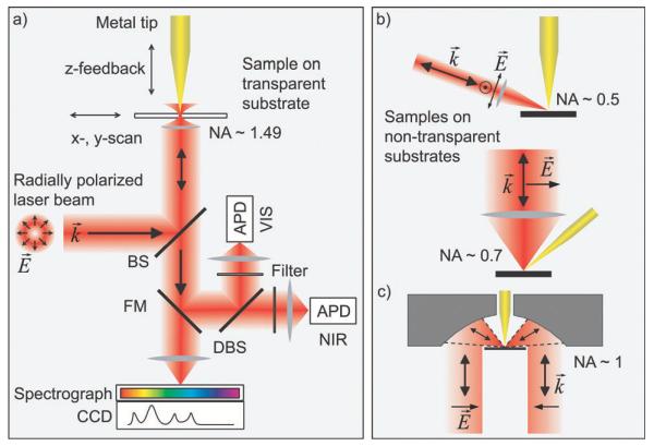
Illumination schemes can be divided in two classes based on their applicability to non-transparent samples (Fig. 6). Side-illumination allows studying non-transparent samples for which the polarization requirement of the tip antenna can be easily fulfilled (Fig. 6(b)). In the case of transparent samples on-axis illumination can benefit from high numerical aperture (NA) objectives with NA > 1 that decrease the size of the confocal volume contributing to the far-field background discussed above in Section 2.3.4 and that maximize the collection efficiency of the emitted light (Fig. 6(a)). The later point is paramount in the case of weakly fluorescence species for which photobleaching at high excitation densities becomes an issue. For on-axis illumination however, light propagation is parallel to the polarization direction required to excite efficient field enhancement in etched wire tips. This requirement can be fulfilled using higher order laser modes.97,98
Fig. 6.
(a) Schematic of an experimental setup employing on-axis illumination of a transparent sample used to observe simultaneous Raman scattering and photoluminescence of carbon nanotubes.21 A sharp metal tip is positioned in a tightly focused radially polarized laser beam. The optical signal is detected either by two avalanche photodiodes (APDs) for the VIS and NIR spectral range or by a combination of a spectrograph and a CCD. (b) Side-illumination of the tip on top of a non-transparent substrate. (c) Focusing of light using a parabolic mirror with high numerical aperture. To generate a strong field component parallel to the tip axis required for efficient field enhancement, scheme (a) and (c) utilize a radially polarized laser mode.97-99
Non-transparent samples can be investigated at high numerical aperture employing parabolic mirror objectives instead of glass objectives (Fig. 6(c)).99-101 Moreover, parabolic mirrors do not exhibit chromatic aberrations and can be used at all temperatures and under UHV conditions. Their alignment is delicate since already minor deviations lead to substantially altered focal fields and reduced detection sensitivity.100 In UHV implementations an external lens can also be used as a focusing element that can be adjusted easily and without affecting the vacuum.102 An alternative approach to investigate opaque samples is the top illumination scheme.50 By making use of a long working distance objective with a high NA the laser can be focused on the tip apex from the top. Here the tip must be held at an angle with respect to the propagation direction.
To acquire an image, the tip is positioned in the focus of the objective and illuminated by laser light. The optical signal is typically collected through the same objective and detected either using sensitive avalanche photodiodes (APDs) or CCD-equipped spectrometers after rejecting the fundamental laser light. Raster scanning the sample then allows for the simultaneous detection of near-field optical signals and of the topography of the sample. Spectroscopic images formed by acquiring spectra at each pixel of the scan provide most detailed information allowing for spectroscopic contrast.
In a simplified view, a tip-enhanced near-field optical microscope is built by combining a confocal microscope with a setup for tip-sample distance control, e.g. an atomic force or a scanning tunneling microscope as mentioned above (see e.g. ref. 96 and 103). While these microscopic techniques are fully developed, their combination certainly adds substantial complexity and will require careful design modifications to achieve a high-degree of user-friendliness. Although there is a huge variety of different probes for AFM, including chemically functionalized and magnetic types, most of the commercially available tips to date cannot be efficiently used for TENOM being based on semiconductor materials that provide only weak signal enhancement (see Section 3.1). At present, the development of well-defined large-scale fabrication processes of metallic or metalized probes with maximized field enhancement factors at high reproducibility and mechanical stability is an important issue.
Coupling an emitter to an optical antenna changes the angular emission according to the directivity of the antenna (see Section 2.2).44,45,104 This has immediate consequences for the actual amount of collected signal. The collection efficiency of the microscope setup is angular and polarization dependent. The collection angle is limited by the NA of the microscope objective. In order to benefit from the antenna-enhanced emission quantified by the antenna gain (eqn (2)), the redirected emission needs to fit within the angular detection range.45,105 Drastic signal loss can occur especially when using objectives with a low NA. The collection efficiency of a detection system can be calculated by
| (7) |
where D(θ, φ) is the directivity of the antenna taking into account the sample substrate. Calculating the collection efficiency for the case of a vertical optical antenna and a horizontal dipolar emitter on glass for an antenna-emitter distance of about 20 nm for two different objectives with a NA of 0.5 and 1.3 reveals a ratio of ηcoll(NA = 1.3)/ηcoll(NA = 0.5) ≈ 0.63/0.017 ≈ 37.105 As a figure of merit for the relative detected fluorescence intensity one can define F = Kradηcoll2 that considers also the excitation efficiency Krad and neglects changes in the quantum efficiency.105 For the objectives with an NA of 0.5 and 1.3 this leads to a ratio of F(NA = 1.3)/F(NA = 0.5) ≈ 1373. For a vertical dipole this ratio is even higher. Note that the field enhancement is strongly dependent on the substrate material (Section 3.1). Using transparent, dielectric substrates can benefit from the high collection efficiency of the axial illumination scheme using high NA objectives (see Fig. 7). However, the field enhancement is typically weaker compared to metallic substrates (see Section 2.2).
In Section 3.1 different antenna designs that aim either at maximizing the enhancement or eliminating the background signal are described. Another possibility to increase the image contrast is to postprocess the signal by suppressing the background. The first approach makes use of the rapid decay of the near-field signal upon increasing tip-sample distance. In this approach a tapping-mode AFM is used to probe the sample while the optical signal is demodulated at the fundamental or higher harmonics of the tapping mode frequency. In the case of weakly emitting samples such as single fluorescent molecules, time-tagging of the detected photons with respect to the tapping oscillation is used to distinguish between photons generated during small tip-sample distances related to dominating near-field interactions and those detected while the tip-sample distance is increased corresponding to far-field contributions.107,108 At present, the corresponding demodulation of CCD-signals is challenging precluding the acquisition of complete spectra at higher harmonic tapping mode frequencies.
A background suppression scheme that also works for tuning fork based systems (due to their high stiffness tuning forks cannot be oscillated at high amplitudes) makes use of an external feedback modulation.109 By adding a periodic modulation to the set point that controls the strength of the interaction between tip and sample, their distance is modulated accordingly. The background signal is then rejected by demodulating the photon count rate with a lock-in amplifier. This scheme can be employed for any scanning probe system using a feedback loop to control the tip-sample distance. A drawback of all background suppression schemes is the loss of signal enhancement, since the emitter stays only a fraction of time in the near-field of the optical antenna.
Usually the tip-sample distance control achieved by shear-force or tapping mode systems is not very accurate and stable making long measurements at a desired tip-sample distance challenging. If one wants to control the tip-sample distance at the subnanometer scale one can make use of a time-gated illumination technique combined with a tapping mode system.110 Here, the laser intensity is modulated such that the sample is illuminated only when the oscillating tip reaches a certain vertical distance. Using this scheme one can preselect a tip-sample distance and perform the measurement at this specific distance with an accuracy of below 1 nm. The time gating can be achieved by synchronizing the trigger signal extracted from the tip oscillation with a pulse generator that controls an acousto-optic modulator acting as an optical shutter.
4 Applications of TENOM
TENOM has been demonstrated for a large variety of sample materials during the last 15 years. Examples range from 0D structures, such as single molecules or quantum dots, 1D structures, such as carbon nanotubes or inorganic semiconducting nanowires to 2D structures like graphene. Depending on the sample material the enhanced and detected signals can be purely optical, such as Raman scattering or fluorescence/photoluminescence, or photoelectrical and photochemical. In the following several examples are reviewed to illustrate the broad applicability and versatility of TENOM.
4.1 Applications of tip-enhanced Raman scattering
Raman scattering probes the characteristic vibrational eigen-modes of materials and is thus capable of delivering valuable chemical information. Of particular interest are studies of biological materials for which functionalities are often directly connected to the molecular structure and conformation. Since biomolecules are typically weak Raman scatterers compared to many crystalline materials the large signal enhancement provided by TERS makes the technique particularly interesting. TERS has been successfully applied to study systems such as RNA and DNA, proteins, collagen, bacteria and viruses as summarized in ref. 111-113. While most of the TER studies so far consist of single point measurements, there are also few high-resolution spatial images of biological samples. One of them is illustrated in Fig. 8. It shows a TER image of a specific Raman band of single nanotapes formed from beta-amyloid(1–40) peptide fragments together with the simultaneously obtained STM image. As marked by the circle and the arrow features that are invisible in the STM image can identified as nanotape structures in the TER image. The authors explain this by the surface sensitivity of TERS: nanotapes of different heights but similar composition show the same contrast in the TERS image but not in the STM image. Wood et al.113 applied TERS to hemoglobin. The authors demonstrated selective enhancement of heme, protein and amino acid modes that help to detect nanoscale oxidation effects at the crystal surface.
Fig. 8.
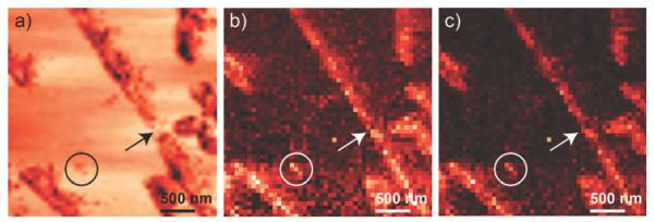
Simultaneously acquired (a) STM and (b and c) TERS (acquisition time 1 s per pixel, 2 mW incident power) images of individual nanotapes formed from beta-amyloid(1–40) peptide fragments (50 × 50 pixels). The color-coded TERS images display the intensity (high intensity is represented by a brighter pixel) of the aromatic ring breathing marker band (1004 cm −1). (b) Value of the peak integral, and (c) peak maximum. The arrow and circle illustrate that areas weakly observed as a feature in the STM image can be identified as nanotape/peptide structures using TERS imaging (Reprinted with permission from ACS Nano, 2013, 7, 911. Copyright 2013 American Chemical Society.).
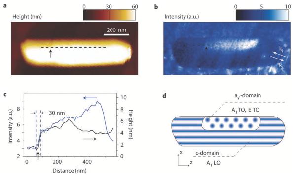
Besides biological materials TERS studies have been performed on different inorganic nanowires such as Ge nanowires114,115 and CdSe nanowires.116 Berweger and co-workers117 extended TERS to optical crystallography. By probing different transverse phonon modes of BaTiO3 nanorods they could spatially resolve ferroelectric domains in the crystal (see Fig. 9).
Fig. 9.
Spatially resolved TERS for ferroelectric domain imaging. (a) Topography of a BaTiO3 nanorod. (b) The spectrally integrated TERS signal for ferroelectric domain imaging. (c) Lateral cross section along the dashed lines in a and b of the region of high TERS signal (blue) and corresponding topography (black) on the rod. (d) Domain assignment based on the Raman selection rules for the TERS geometry used (figure reproduced with permission from ref. 117, ©2009 NPG.).
Motivated by the ongoing device miniaturization in information technology reaching nanometer length scales, the applicability of TERS to structured semiconductor surfaces has been investigated by several groups.118-120 Here Raman spectroscopy is of particular interest since engineered stress/strain fields used to tune charge carrier mobilities in devices could be visualized by probing local phonon energies. Such studies, however, are impeded by the the significant signal background from the bulk (see Section 4). By selecting the polarization of the excitation and the detected scattered light phonon selection rules can be exploited to increase the near-field to far-field contrast.119,121 In addition to local field enhancement depolarization due to scattering from the tip can play a significant role in the enhancement process contributing to the complexity of a quantitative analysis of the image contrast.119 This also underlines the importance of tip-sample distance curves to identify the nature and range of the interaction mechanism.
In the past ten years TERS has been demonstrated to be particularly well suited for the studies of graphitic materials such as single-walled carbon nanotubes (SWCNTs), multi-walled carbon nanotubes (MWCNTs) and graphene (see e.g. ref. 122-125). These materials feature rich phonon and electron–phonon coupling physics making Raman spectroscopy a very useful tool. In addition, these materials are photochemically stable and render clear topographic signatures that can be used for their precise non-optical localization. TERS has been used to study defects and structural variations along single SWCNTs,124,126 the effects of local pressure127 and the influence of doping on the electron dispersion.122
4.2 Applications of tip-enhanced fluorescence
Fluorescence spectra and transients reflect the energy and population – relaxation dynamics of photoexcited states. Tip-enhanced fluorescence microscopy has the potential to provide access to these material properties on nanometer length scales. Moreover, the local enhancement of excitation and emission can also be used to obtain information on the mobility and spatial extension of photoexcited states.
Single fluorescent molecules can be treated as point-like dipolar absorbers and emitters. The excitation and emission rate is proportional to the squared scalar product between the local electric field and transition dipole moment of the molecule. Single molecules can thus be used to probe the vectorial field distribution in the vicinity of the antenna. Following the discussion of the signal enhancement in Section 2.3.2 the resulting fluorescence intensity patterns will also reflect the tip-sample distance dependent quenching by the metal antenna.43,76 From the discussion in Section 2.3.2 it is evident that tip-enhanced fluorescence is most efficient for emitters with low quantum yield.23,36 Luminescent inorganic nanocrystals or quantum dots have been used for similar studies by various groups.33,39,43,128,129
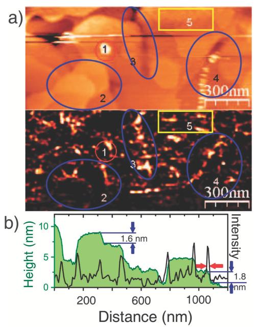
TENOM has been applied to study thin organic films. Zhang et al.93 recorded tip-enhanced photoluminescence images of a semiconductor film made of diindenperylene on silicon simultaneously with the topography (see Fig. 10). A 6 × 10⁵ times enhanced photoluminescence was found at the domain boundaries (regions labeled with 2–4) with an absorption enhancement of 4 × 10⁴ and an emission enhancement of 15. The authors explain the enhanced PL yield by an increased coupling between the tip plasmon and the exciton polariton in the film.
Fig. 10.
(a) Simultaneously recorded topographic (upper panel) and near-field optical images (lower panel). Laser power: 170 μW. Tip-sample distance: 3 nm. (b) Line profile through the topographic image with its correlated optical intensity. Strongest emission dominated by PL from the DIP film is observed at terraces. Emission spectra show additional characteristic Raman bands of DIP and a broad PL background from the gold tip used in the experiment (Reprinted with permission from D. Zhang et al. Phys. Rev. Lett., 2010, 104, 056601. Copyright (2010) by the American Physical Society.).
Besides single molecules and thin films tip-enhanced fluorescence is suitable to investigate 1D-systems such as inorganic semiconducting nanowires and nanorods due to the favorable volume ratio. Yoskovitz et al.39 investigated the interaction of an AFM tip with single CdSe/CdS quantum dots and CdSe/CdS nanorods by studying their lifetime and intensity characteristics. Simultaneous tip-enhanced PL and Raman imaging along individual CdSe nanowires at a spatial resolution of about 20 nm is presented by Böhmler and co-workers.116 By hyperspectral imaging variations in the PL energy and intensity along individual nanowires were mapped tentatively attributed to nano-scale phase variations with alternating wurtzite and zincblende segments that cannot be resolved by confocal microscopy. Indium phosphide nanowires were studied by Bao et al.89 using a nano-fabricated campanile tip. Enhanced PL measurements revealed spatially varying emission energies and intensities reflecting local charge recombination heterogeneities.
Tip-enhanced PL measurements have been used for a number of studies on single-walled carbon nanotubes.21,122 Example include investigations on the influence of DNA wrapping on the local emission energy and on the energy transfer between nanotubes in a thin bundle.96,130 Quenching of mobile exciton states by the nanotube ends and the competition between local emission enhancement and exciton mobility was studied and modelled qualitatively by Georgi and co-workers.131
4.3 Tip-enhanced photocurrent microscopy
Due to the size-mismatch between the wavelength of visible light and the dimensions of nanoscale optoelectronic devices comprising novel materials such as e.g. inorganic nanowires or nanotubes, the full potential of these devices could not be exploited so far. For the same reason the details of the electrical-to-optical and optical-to-electrical transduction mechanisms remain hidden in conventional optical microscopy. Using optical antennas the performance of nanoscale optoelectronic devices could thus be improved and, if the antenna is scanned across the sample in close proximity, high-resolution images could be obtained.7,132
In most materials direct optical transitions connect charge neutral ground and excited states. Optical excitation of inorganic nanowires and carbon nanotubes predominately leads to the formation of excitons that are also the states dominating photoluminescence. Photocurrent and electroluminescence are phenomena that directly connect these optical excitations to the separation and recombination of charge carriers, respectively.
Fig. 11 illustrates how tip-enhanced photocurrent microscopy can be used to study the optoelectronic properties of a carbon nanotube device with nanoscale resolution. Simultaneous hyper-spectral Raman imaging probing different phonon modes provides complementary structural information.
Fig. 11.
Antenna-enhanced imaging of photocurrent fluctuations along a single SWCNT device. (a) Topography image. The drain and source electrodes appear at the top and at the bottom of the image. (b and c) Antenna-enhanced photocurrent and Raman G-band image. The dashed yellow line marks the position of the central particle. (d) The integrated photocurrent signal from panel d after a slope subtraction (blue symbols). The local minimum and kinks in the band energy profile seen in panels d and e coincide with the locations of particles seen as peaks in the topography data (black curve in panel e and marked in panel d by dashed vertical lines). (e) Schematic band diagram. The local minimum cannot be resolved with a diffraction limited laser spot due to spatial averaging of photocurrent signals with opposite signs. (f) High-resolution spectroscopic imaging of the central region of the device showing the topography, photocurrent, Raman D-band intensity and Raman G-band intensity. A varying defect induced D-band signal strength can be observed along the SWCNT, but without showing a correlation with the photocurrent signal (Reprinted with permission from ACS Nano, 2012, 6, 6416. Copyright 2012 American Chemical Society.).
The multi-modal detection in Fig. 11 combining photocurrent, topography and full spectroscopic Raman mapping could potentially be extended further by the large set of scanning probe techniques. As pointed out by Burghard and Mews133 the antenna could also be used as a local electrical gate or for detecting electrostatic forces (electrostatic force microscopy (EFM), or Kelvin probe microscopy (KPM)). By biasing a metal coated tetrahedral glass tip (see Section 3.1) Gerster and co-authors134 detected the photocurrent of single photosynthetic proteins further highlighting the versatility of the optical antenna scheme.
5 Conclusions
The results presented in this review illustrate that tip-enhanced near-field optical microscopy (TENOM) has developed into a very powerful and highly versatile tool for the spectroscopic investigation of nanoscale materials on surfaces. Conceptual developments, in particular the treatment of the enhancement provided by the tip as an antenna effect and the definition of the key characteristics of an optical antenna, substantially improved our understanding of the underlying mechanism and stimulated the design of novel antenna structures. Moreover, from the antenna concept signal enhancement schemes for photovoltaics and electrically driven light emission follow naturally. Besides a broad range of purely optical information TENOM can thus also provide spatially correlated optoelectronic information. With this tool details of the optical-to-electrical and electrical-to-optical transduction in nanoscale devices and hybrid materials could be investigated for the first time on relevant nanometer length scales. Being a scanning-probe approach TENOM can be readily combined with other SPM techniques such as electrostatic force and scanning gate microscopy. Due to this multi-mode capability TENOM can be expected to become of particular relevance for the functional characterization of photovoltaic materials and device architectures used for light energy harvesting.
At present active research in the field of TENOM focuses on several directions: first, the continuing expansion of our pool of optical antenna probes and their optimization regarding size, gain and directivity as well as ease of fabrication and reproducibility. Second, an improved understanding of plasmonic phenomena at very short length scales and the contributions of quantum phenomena. Third, the combination with other scanning probe as well as time-resolved optical techniques. All these activities and developments will further advance TENOM with respect to wide-range applicability, signal enhancement and spatial resolution.
Acknowledgements
We thank our collaborators in this field of research. Projects were financially supported by the ERC through the starting grant NEWNANOSPEC and the Deutsche Forschungsgemeinschaft (DFG) through the Nanosystems Initiative Munich (NIM).
Biographies
Nina Mauser

Nina Mauser studied physics at the LMU München, Germany, and Lund University, Sweden. She performed her diploma thesis in the field of ultracold atoms and molecules at the UBC Vancouver, Canada. In 2010 she started her PhD in the nanooptics group of Achim Hartschuh at the LMU München. Currently she focuses on antenna-enhanced optoelectronic probing of 1D nanostructures.
Achim Hartschuh

Achim Hartschuh studied Physics at the Universities of Tübingen and Stuttgart, Germany, and received his PhD in 2001 with Prof. H. C. Wolf. He spent two years carrying out postdoctoral research at The Institute of Optics at the University of Rochester, New York, USA, in the research group of Prof. L. Novotny. In 2002 he became Junior Professor at the University of Siegen and moved after two years to the University of Tübingen. Since 2006 he has been Professor at the LMU München, Germany. His research focuses on the understanding of light-matter interactions on short length scales and the development and application of new techniques for optical imaging and spectroscopy with nanoscale spatial and femtosecond temporal resolution.
References
- 1.Novotny L. Progress in Optics. In: Wolf E, editor. Vol. 50. Elsevier; Amsterdam, The Netherlands: 2007. p. 137. [Google Scholar]
- 2.Hartschuh A. Angew. Chem., Int. Ed. 2008;47:8178. doi: 10.1002/anie.200801605. [DOI] [PubMed] [Google Scholar]
- 3.Yeo BS, Stadler J, Schmid T, Zenobi R, Zhang W. Chem. Phys. Lett. 2009;472:1. [Google Scholar]
- 4.Ming T, Chen H, Jiang R, Li Q, Wang F. J. Phys. Chem. Lett. 2012;3:191. [Google Scholar]
- 5.Pettinger B, Schambach P, Villagómez CJ, Scott N. Annu. Rev. Phys. Chem. 2012;63:379. doi: 10.1146/annurev-physchem-032511-143807. [DOI] [PubMed] [Google Scholar]
- 6.Atkin JM, Berweger S, Jones AC, Raschke MB. Adv. Phys. 2012;61:745. [Google Scholar]
- 7.Bharadwaj P, Deutsch B, Novotny L. Adv. Opt. Photonics. 2009;1:438. [Google Scholar]
- 8.Agio M, Alú A, editors. Optical Antennas. Cambridge University Press; Cambridge: 2013. [Google Scholar]
- 9.Novotny L, van Hulst N. Nat. Photonics. 2011;5:83. [Google Scholar]
- 10.Novotny L, Hecht B. Principles of nano-optics. Cambridge University Press; Cambridge: 2006. [Google Scholar]
- 11.Betzig E, Chichester RJ. Science. 1993;262:1422. doi: 10.1126/science.262.5138.1422. [DOI] [PubMed] [Google Scholar]
- 12.Michaelis J, Hettich C, Mlynek J, Sandoghdar V. Nature. 2000;405:325. doi: 10.1038/35012545. [DOI] [PubMed] [Google Scholar]
- 13.Kühn S, Hettich C, Schmitt C, Poizat JP, Sandoghdar V. J. Microsc. 2000;202:2. doi: 10.1046/j.1365-2818.2001.00829.x. [DOI] [PubMed] [Google Scholar]
- 14.Stöhr RJ, Kolesov R, Xia K, Reuter R, Meijer J, Logvenov G, Wrachtrup J. ACS Nano. 2012;6:9175. doi: 10.1021/nn303510p. [DOI] [PubMed] [Google Scholar]
- 15.Olomon RL, Raschke MB. Nanotechnology. 2012;23:444001. doi: 10.1088/0957-4484/23/44/444001. [DOI] [PubMed] [Google Scholar]
- 16.Nie S, Emory SR. Science. 1997;275:1102. doi: 10.1126/science.275.5303.1102. [DOI] [PubMed] [Google Scholar]
- 17.Xu H, Aizpurua J, Käll M, Apell P. Phys. Rev. E. 2000;62:4318. doi: 10.1103/physreve.62.4318. [DOI] [PubMed] [Google Scholar]
- 18.Baker GA, Moore DS. Anal. Bioanal. Chem. 2005;382:1751. doi: 10.1007/s00216-005-3353-7. [DOI] [PubMed] [Google Scholar]
- 19.Zhang R, Zhang Y, Dong ZC, Jiang S, Zhang C, Chen LG, Zhang L, Liao Y, Aizpurua J, Luo Y, Yang JL, Hou JG. Nature. 2013;498:82. doi: 10.1038/nature12151. [DOI] [PubMed] [Google Scholar]
- 20.Berweger S, Raschke MB. Anal. Bioanal. Chem. 2010;396:115. doi: 10.1007/s00216-009-3085-1. [DOI] [PubMed] [Google Scholar]
- 21.Hartschuh A, Qian H, Meixner AJ, Anderson N, Novotny L. Nano Lett. 2005;5:2310. doi: 10.1021/nl051775e. [DOI] [PubMed] [Google Scholar]
- 22.Aslan K, Gryczynski I, Malicka J, Matveea E, Lakowicz JR, Geddes CD. Anal. Biotechnol. 2005;16:55. doi: 10.1016/j.copbio.2005.01.001. [DOI] [PMC free article] [PubMed] [Google Scholar]
- 23.Bharadwaj P, Novotny L. J. Phys. Chem. C. 2010;114:7444. [Google Scholar]
- 24.Chance RR, Prock A, Silbey R. J. Chem. Phys. 1974;60:2744. [Google Scholar]
- 25.Barnes WL. J. Mod. Opt. 1998;45:661. [Google Scholar]
- 26.Thomas M, Carminati R, Arias-Gonzalez JR, Greffet J-J. Appl. Phys. Lett. 2004;85:3863. [Google Scholar]
- 27.Bek A, Jansen R, Ringler M, Mayilo S, Klar TA, Feldmann J. Nano Lett. 2005;5:585. doi: 10.1021/nl072602n. [DOI] [PubMed] [Google Scholar]
- 28.Carminati R, Greffet JJ, Henkel C, Vigoureux JM. Opt. Commun. 2006;261:368. [Google Scholar]
- 29.Issa NA, Guckenberger R. Opt. Express. 2007;15:12131. doi: 10.1364/oe.15.012131. [DOI] [PubMed] [Google Scholar]
- 30.Rogobete L, Kaminski F, Agio M, Sandoghdar V. Opt. Lett. 2007;32:1623. doi: 10.1364/ol.32.001623. [DOI] [PubMed] [Google Scholar]
- 31.Baffou G, Girard C, Dujardin E, Colas des Francs G, Martin OJF. Phys. Rev. B: Condens. Matter Mater. Phys. 2008;77:121101(R). [Google Scholar]
- 32.Kern AM, Meixner AJ, Martin OJF. ACS Nano. 2012;6:9828. doi: 10.1021/nn3033612. [DOI] [PubMed] [Google Scholar]
- 33.Farahani JN, Pohl DW, Eisler H-J, Hecht B. Phys. Rev. Lett. 2005;95:017402. doi: 10.1103/PhysRevLett.95.017402. [DOI] [PubMed] [Google Scholar]
- 34.Anger P, Bharadwaj P, Novotny L. Phys. Rev. Lett. 2006;96:113002. doi: 10.1103/PhysRevLett.96.113002. [DOI] [PubMed] [Google Scholar]
- 35.Kühn S, Hakanson U, Rogobete L, Sandoghdar V. Phys. Rev. Lett. 2006;97:017402. doi: 10.1103/PhysRevLett.97.017402. [DOI] [PubMed] [Google Scholar]
- 36.Bharadwaj P, Anger P, Novotny L. Nanotechnology. 2007;18:044017. [Google Scholar]
- 37.Eckel R, Walhorn V, Pelargus C, Martini J, Enderlein J, Nann T, Anselmetti D, Ros R. Small. 2007;3:44. doi: 10.1002/smll.200600130. [DOI] [PubMed] [Google Scholar]
- 38.Bek A, Jansen R, Ringler M, Mayilo S, Klar TA, Feldmann J. Nano Lett. 2008;8:485. doi: 10.1021/nl072602n. [DOI] [PubMed] [Google Scholar]
- 39.Yoskovitz E, Hadar I, Sitt A, Lieberman I, Banin U. J. Phys. Chem. C. 2009;115:15834. [Google Scholar]
- 40.Mohammadi A, Sandoghdar V, Agio M. New J. Phys. 2008;10:105015. [Google Scholar]
- 41.Stavola M, Dexter DL, Knox RS. Phys. Rev. B: Condens. Matter Mater. Phys. 1985;31:2277. doi: 10.1103/physrevb.31.2277. [DOI] [PubMed] [Google Scholar]
- 42.Azoulay J, Débarre A, Richard A, Tchénio P. Europhys. Lett. 2000;51:374. [Google Scholar]
- 43.Shafran E, Mangum BD, Gerton JM. Phys. Rev. Lett. 2011;107:037403. doi: 10.1103/PhysRevLett.107.037403. [DOI] [PubMed] [Google Scholar]
- 44.Taminiau TH, Stefani FD, Segerink FB, van Hulst NF. Nat. Photonics. 2008;2:234. [Google Scholar]
- 45.Böhmler M, Hartmann N, Georgi C, Hennrich F, Hersam MC, Hartschuh A. Opt. Express. 2010;18:16443. doi: 10.1364/OE.18.016443. [DOI] [PubMed] [Google Scholar]
- 46.Eghlidi H, Lee KG, Chen X-W, Götzinger S, Sandoghdar V. Nano Lett. 2009;9:4007. doi: 10.1021/nl902183y. [DOI] [PubMed] [Google Scholar]
- 47.Roy D, Wang C, Williams J. J. Appl. Phys. 2009;105:013530. [Google Scholar]
- 48.Kawata S, Shalaev VM, editors. Tip enhancement. Elsevier; Amsterdam: 2007. [Google Scholar]
- 49.Ren B, Picardi G, Pettinger B. Rev. Sci. Instrum. 2004;75:837. [Google Scholar]
- 50.Stadler J, Schmid T, Zenobi R. Nano Lett. 2010;10:4514. doi: 10.1021/nl102423m. [DOI] [PubMed] [Google Scholar]
- 51.Lopes M, Toury T, de La Chapelle M, Bonaccorso F, Gucciardi PG. Rev. Sci. Instrum. 2013;84:073702. doi: 10.1063/1.4812365. [DOI] [PubMed] [Google Scholar]
- 52.Demings AL, Festy F, Richards D. J. Chem. Phys. 2005;122:184716. doi: 10.1063/1.1896356. [DOI] [PubMed] [Google Scholar]
- 53.Roy D, Williams C, Mingard K. J. Vac. Sci. Technol., B. 2010;28:631. [Google Scholar]
- 54.Deckert-Gaudig T, Deckert V. Small. 2009;5:432. doi: 10.1002/smll.200801237. [DOI] [PubMed] [Google Scholar]
- 55.Huang J-S, Callegari V, Geisler P, Brüning C, Kern J, Prangsma JC, Wu X, Feichtner T, Ziegler J, Weinmann P, Kamp M, Forchel A, Biagioni P, Sennhauser U, Hecht B. Nat. Commun. 2010;1:150. doi: 10.1038/ncomms1143. [DOI] [PubMed] [Google Scholar]
- 56.Neascu CC, Steudle GA, Raschke MB. Appl. Phys. B: Lasers Opt. 2005;80:295–300. [Google Scholar]
- 57.Neascu CC, Reider GA, Raschke MB. Phys. Rev. B: Condens. Matter Mater. Phys. 2005;71:201402(R). [Google Scholar]
- 58.Thomas S, Krüger M, Föster M, Schenk M, Hommelhoff P. 2012 arXiv: 1209.5195vl. [Google Scholar]
- 59.Kalkbrenner T, Ramstein M, Mlynek J, Sandoghdar V. J. Microsc. 2001;202:72. doi: 10.1046/j.1365-2818.2001.00817.x. [DOI] [PubMed] [Google Scholar]
- 60.Barsegova I, Lewis A, Khatchatouriants A, Manevitch A, Ignatov A, Axelrod N, Sukenik C. Appl. Phys. Lett. 2002;81:3461. [Google Scholar]
- 61.Vakarelski IU, Higashitani K. Langmuir. 2006;22:2931. doi: 10.1021/la0528145. [DOI] [PubMed] [Google Scholar]
- 62.Bharadwaj P, Novotny L. Opt. Express. 2007;15:14266. doi: 10.1364/oe.15.014266. [DOI] [PubMed] [Google Scholar]
- 63.Deeb C, Zhou X, Plain J, Wiederrecht GP, Bachelot R. J. Phys. Chem. C. 2013;117:10669. [Google Scholar]
- 64.Stockman MI, Bergman DJ. Phys. Rev. Lett. 2003;91:227402. doi: 10.1103/PhysRevLett.91.227402. [DOI] [PubMed] [Google Scholar]
- 65.Höppener C, Lapin ZJ, Bharadwaj P, Novotny L. Phys. Rev. Lett. 2012;109:017402. doi: 10.1103/PhysRevLett.109.017402. [DOI] [PubMed] [Google Scholar]
- 66.Sinjab F, Lekprasert B, Woolley RA, Roberts CJ, Tendler SJB, Notingher I. Opt. Lett. 2012;37:2256. doi: 10.1364/OL.37.002256. [DOI] [PubMed] [Google Scholar]
- 67.Johnson TW, Lapin ZJ, Beams R, Lindquist NC, Rodrigo SG, Novotny L, Oh S-H. ACS Nano. 2012;6:9168. doi: 10.1021/nn303496g. [DOI] [PubMed] [Google Scholar]
- 68.Yeo BS, Schmid T, Zhang W, Zenobi R. Anal. Bioanal. Chem. 2007;387:2655. doi: 10.1007/s00216-007-1165-7. [DOI] [PubMed] [Google Scholar]
- 69.Bailo E, Deckert V. Angew. Chem., Int. Ed. 2008;47:1658. doi: 10.1002/anie.200704054. [DOI] [PubMed] [Google Scholar]
- 70.Novotny L. Phys. Rev. Lett. 2007;98:266802. doi: 10.1103/PhysRevLett.98.266802. [DOI] [PubMed] [Google Scholar]
- 71.Taminiau TH, Moerland RJ, Segerink FB, Kuipers L, van Hulst NF. Nano Lett. 2007;7:28. doi: 10.1021/nl061726h. [DOI] [PubMed] [Google Scholar]
- 72.Bharadwaj P, Beams R, Novotny L. Chem. Sci. 2011;2:136. [Google Scholar]
- 73.Schuck PJ, Fromm DP, Sundaramurthy A, Kino GS, Moerner WE. Phys. Rev. Lett. 2005;94:017402. doi: 10.1103/PhysRevLett.94.017402. [DOI] [PubMed] [Google Scholar]
- 74.Farahani JN, Eisler H-J, Pohl DW, Pavius M, Flückiger P, Gasser B, Hecht P. Nanotechnology. 2007;18:125506. [Google Scholar]
- 75.Kinkhabwala A, Zongfu Y, Shanhui F, Avlasevich Y, Müllen K, Moerner WE. Nat. Photonics. 2009;3:654. [Google Scholar]
- 76.Mivelle M, van Zanten TS, Neumann L, van Hulst NF, Garcia-Parajo MF. Nano Lett. 2012;12:5972. doi: 10.1021/nl303440w. [DOI] [PubMed] [Google Scholar]
- 77.Frey HG, Keilmann F, Kriele A, Guckenberger R. Appl. Phys. Lett. 2002;81:530. [Google Scholar]
- 78.Frey HG, Witt S, Felderer K, Guckenberger R. Phys. Rev. Lett. 2004;93:200801. doi: 10.1103/PhysRevLett.93.200801. [DOI] [PubMed] [Google Scholar]
- 79.Ropers C, Neacsu CC, Elsaesser T, Albrecht M, Raschke MB, Lienau C. Nano Lett. 2007;7:2784. doi: 10.1021/nl071340m. [DOI] [PubMed] [Google Scholar]
- 80.De Angelis F, Das G, Candeloro P, Patrini M, Galli M, Bek A, Maksymov I, Liberale C, Andreani LC, Di Fabrizio E. Nat. Nanotechnol. 2010;5:67. doi: 10.1038/nnano.2009.348. [DOI] [PubMed] [Google Scholar]
- 81.Eckert JM, an Freyland R, Gersen H, Heinzelmann H, Schürmann G, Noell W, Staufer U, de Rooij NF. Appl. Phys. Lett. 2000;77:3695. [Google Scholar]
- 82.Bouhelier A, Renger J, Beversluis MR, Novotny L. J. Microsc. 2003;210:220. doi: 10.1046/j.1365-2818.2003.01108.x. [DOI] [PubMed] [Google Scholar]
- 83.Bortchagovsky EG, Klein S, Fischer UC. Appl. Phys. Lett. 2009;94:063118. [Google Scholar]
- 84.Koglin J, Fischer UC, Fuchs H. Phys. Rev. B: Condens. Matter Mater. Phys. 1997;55:7977. [Google Scholar]
- 85.Tanaka K, Burr GW, Grosjean T, Maletzky T, Fischer UC. Appl. Phys. B: Lasers Opt. 2008;93:257. [Google Scholar]
- 86.Leinhos T, Rudow O, Stopka M, Vollkopf A, Oesterschulze E. J. Microsc. 1999;194:349. doi: 10.1046/j.1365-2818.1999.00538.x. [DOI] [PubMed] [Google Scholar]
- 87.Weber-Bargioni A, Schwartzberg A, Cornaglia M, Ismach A, Urban JJ, Pang Y, Gordon R, Bokor J, Salmeron MB, Ogletree DF, Ashby P, Cabrini S, Schuck PJ. Nano Lett. 2011;11:1201. doi: 10.1021/nl104163m. [DOI] [PubMed] [Google Scholar]
- 88.Bao W, Staffaroni M, Bokor J, Salmeron MB, Yablonovitch E, Cabrini S, Weber-Bargioni A, Schuck PJ. Opt. Express. 2013;21:8166. doi: 10.1364/OE.21.008166. [DOI] [PubMed] [Google Scholar]
- 89.Bao W, Melli M, Caselli N, Riboli F, Wiersma DS, Staffaroni M, Choo H, Olgetree DF, Aloni S, Bokor J, Cabrini S, Intonti F, Salmeron MB, Yablonovitch E, Schuck PJ, Weber-Bargioni A. Science. 2012;338:1317. doi: 10.1126/science.1227977. [DOI] [PubMed] [Google Scholar]
- 90.Notingher I, Elfick A. J. Phys. Chem. B. 2005;109:15699. doi: 10.1021/jp0523120. [DOI] [PubMed] [Google Scholar]
- 91.Chen X-W, Agio M, Sandoghdar V. Phys. Rev. Lett. 2012;108:233001. doi: 10.1103/PhysRevLett.108.233001. [DOI] [PubMed] [Google Scholar]
- 92.Pettinger B, Domke KF, Zhang D, Picardi G, Schuster R. Surf. Sci. 2009;603:1335. [Google Scholar]
- 93.Zhang D, Heinemeyer U, Stanciu C, Sackrow M, Braun K, Hennemann LE, Wang X, Scholz R, Schreiber F, Meixner AJ. Phys. Rev. Lett. 2010;104:056601. doi: 10.1103/PhysRevLett.104.056601. [DOI] [PubMed] [Google Scholar]
- 94.Karrai K, Grober RD. Appl. Phys. Lett. 1995;66:1842. [Google Scholar]
- 95.Pettinger B, Ren B, Picardi G, Schuster R, Ertl G. Phys. Rev. Lett. 2004;92:096101. doi: 10.1103/PhysRevLett.92.096101. [DOI] [PubMed] [Google Scholar]
- 96.Qian H, Georgi C, Anderson N, Green AA, Hersam MC, Novotny L, Hartschuh A. Nano Lett. 2008;8:1363. doi: 10.1021/nl080048r. [DOI] [PubMed] [Google Scholar]
- 97.Novotny L, Sánchez EJ, Xie XS. Ultramicroscopy. 1998;71:21. [Google Scholar]
- 98.Quabis S, Dorn R, Glöckl O, Eberler M, Leuchs G. Opt. Commun. 2000;179:1. [Google Scholar]
- 99.Sackrow M, Stanciu C, Lieb MA, Meixner AJ. ChemPhysChem. 2008;9:316. doi: 10.1002/cphc.200700723. [DOI] [PubMed] [Google Scholar]
- 100.Lieb A, Meixner AJ. Opt. Express. 2001;8:458. doi: 10.1364/oe.8.000458. [DOI] [PubMed] [Google Scholar]
- 101.Steidtner J, Pettinger B. Rev. Sci. Instrum. 2007;78:103104. doi: 10.1063/1.2794227. [DOI] [PubMed] [Google Scholar]
- 102.Jiang N, Foley ET, Klingsporn JM, Sonntag MD, Valley NA, Dieringer JA, Seideman T, Schatz GC, Hersam MC, Van Duyne RP. Nano Lett. 2012;12:5061. doi: 10.1021/nl2039925. [DOI] [PubMed] [Google Scholar]
- 103.Stadler J, Schmid T, Zenobi R. Nanoscale. 2012;4:1856. doi: 10.1039/c1nr11143d. [DOI] [PubMed] [Google Scholar]
- 104.Kühn S, Sandoghdar V. Appl. Phys. B: Lasers Opt. 2006;84:211. [Google Scholar]
- 105.Taminiau TH, Stefani FD, van Hulst NF. New J. Phys. 2008;10:105005. [Google Scholar]
- 106.Enderlein J, Ruckstuhl S, Seeger T. Appl. Opt. 1999;38:724. doi: 10.1364/ao.38.000724. [DOI] [PubMed] [Google Scholar]
- 107.Ma Z, Gerton JM, Wade LA, Quake SR. Phys. Rev. Lett. 2006;97:260801. doi: 10.1103/PhysRevLett.97.260801. [DOI] [PubMed] [Google Scholar]
- 108.Yano T, Ichimura T, Taguchi A, Hayazawa N, Verma P, Inouye Y, Kawata S. Appl. Phys. Lett. 2007;91:121101. [Google Scholar]
- 109.Höppner C, Beams R, Novotny L. Nano Lett. 2009;9:903. doi: 10.1021/nl803903f. [DOI] [PMC free article] [PubMed] [Google Scholar]
- 110.Ichimura T, Fujii S, Verma P, Yano T, Ynouye Y, Kawata S. Phys. Rev. Lett. 2009;102:18601. doi: 10.1103/PhysRevLett.102.186101. [DOI] [PubMed] [Google Scholar]
- 111.Yeo B-S, Stadler J, Schmid T, Zenobi R, Zhang W. Chem. Phys. Lett. 2009;472:1. [Google Scholar]
- 112.Lucas M, Riedo E. Rev. Sci. Instrum. 2012;83:061101. doi: 10.1063/1.4720102. [DOI] [PubMed] [Google Scholar]
- 113.Wood BR, Asghari-Khiavi M, Bailo E, McNaughton D, Deckert V. Nano Lett. 2012;12:1555. doi: 10.1021/nl2044106. [DOI] [PubMed] [Google Scholar]
- 114.Ogawa Y, Yuasa Y, Minami F, Oda S. Appl. Phys. Lett. 2011;99:053112. [Google Scholar]
- 115.Reparaz JS, Peica N, Kirste R, Goni AR, Wagner MR, Callsen G, Alonso MI, Garriga M, Marcus IC, Ronda A, Berbezier I, Maultzsch J, Thomsen C, Hoffmann A. Nanotechnology. 2013;24:185704. doi: 10.1088/0957-4484/24/18/185704. [DOI] [PubMed] [Google Scholar]
- 116.Böhmler M, Wang Z, Myalitsin A, Mews A, Hartschuh A. Angew. Chem., Int. Ed. 2011;50:11536. doi: 10.1002/anie.201105217. [DOI] [PubMed] [Google Scholar]
- 117.Berweger S, Neacsu CC, Mao Y, Zhou H, Wong SS, Raschke MB. Nat. Nanotechnol. 2009;4:496. doi: 10.1038/nnano.2009.190. [DOI] [PubMed] [Google Scholar]
- 118.Hermann P, Hecker M, Chumakov D, Weisheit M, Rinderknecht J, Shelaev A, Dorozhkin P, Eng L. Ultramicroscopy. 2011;111:1630. doi: 10.1016/j.ultramic.2011.08.009. [DOI] [PubMed] [Google Scholar]
- 119.Merlen A, Valmalette JC, Gucciardi PG, Lamy de la Chapelle M, Frigout A, Ossikovski R. J. Raman Spectrosc. 2009;40:1361. [Google Scholar]
- 120.Tarun A, Hayazawa N, Motohashi M, Kawata S. Rev. Sci. Instrum. 2007;79:913706. doi: 10.1063/1.2832347. [DOI] [PubMed] [Google Scholar]
- 121.Berweger S, Raschke MB. J. Raman Spectrosc. 2009;40:1413. [Google Scholar]
- 122.Maciel IO, Anderson N, Pimenta MA, Hartschuh A, Qian H, Terrones M, Terrones H, Campos-Delgado J, Rao AM, Novotny L, Jorio A. Nat. Mater. 2008;7:878. doi: 10.1038/nmat2296. [DOI] [PubMed] [Google Scholar]
- 123.Cancado LG, Jorio A, Ismach A, Joselevich E, Hartschuh A, Novotny L. Phys. Rev. Lett. 2009;103:186101. doi: 10.1103/PhysRevLett.103.186101. [DOI] [PubMed] [Google Scholar]
- 124.Georgi C, Hartschuh A. Appl. Phys. Lett. 2010;97:143117. [Google Scholar]
- 125.Stadler J, Schmid T, Zenobi R. ACS Nano. 2011;5:8442. doi: 10.1021/nn2035523. [DOI] [PubMed] [Google Scholar]
- 126.Anderson N, Hartschuh A, Novotny L. Nano Lett. 2007;7:577. doi: 10.1021/nl0622496. [DOI] [PubMed] [Google Scholar]
- 127.Yano T, Verma P, Saito Y, Ichimura T, Kawata S. Nat. Photonics. 2009;3:473. [Google Scholar]
- 128.Huang FM, Festy F, Richards D. Appl. Phys. Lett. 2005;87:183101. [Google Scholar]
- 129.Yoskovitz E, Oron D, Shweky I, Banin U. J. Phys. Chem. C. 2008;112:16306. [Google Scholar]
- 130.Qian H, Araujo PT, Georgi C, Gokus T, Hartmann N, Green AA, Jorio A, Hersam MC, Novotny L, Hartschuh A. Nano Lett. 2008;8:2706. doi: 10.1021/nl801038t. [DOI] [PubMed] [Google Scholar]
- 131.Georgi C, Green AA, Hersam MC, Hartschuh A. ACS Nano. 2010;4:5914. doi: 10.1021/nn101443d. [DOI] [PubMed] [Google Scholar]
- 132.Schuller JA, Barnard ES, Cai W, Jun YC, White SW, Brongersma ML. Nat. Mater. 2010;9:193. doi: 10.1038/nmat2630. [DOI] [PubMed] [Google Scholar]
- 133.Burghard M, Mews A. ACS Nano. 2012;6:5752. doi: 10.1021/nn3029088. [DOI] [PubMed] [Google Scholar]
- 134.Gerster D, Reichert J, Bi H, Barth JV, Kaniber SM, Holleitner AW, Visolay-Fisher I, Sergani S, Carmeli I. Nat. Nanotechnol. 2012;7:673. doi: 10.1038/nnano.2012.165. [DOI] [PubMed] [Google Scholar]


