Abstract
We report a broadband polarization-independent perfect absorber with wide-angle near unity absorbance in the visible regime. Our structure is composed of an array of thin Au squares separated from a continuous Au film by a phase change material (Ge2Sb2Te5) layer. It shows that the near perfect absorbance is flat and broad over a wide-angle incidence up to 80° for either transverse electric or magnetic polarization due to a high imaginary part of the dielectric permittivity of Ge2Sb2Te5. The electric field, magnetic field and current distributions in the absorber are investigated to explain the physical origin of the absorbance. Moreover, we carried out numerical simulations to investigate the temporal variation of temperature in the Ge2Sb2Te5 layer and to show that the temperature of amorphous Ge2Sb2Te5 can be raised from room temperature to > 433 K (amorphous-to-crystalline phase transition temperature) in just 0.37 ns with a low light intensity of 95 nW/μm2, owing to the enhanced broadband light absorbance through strong plasmonic resonances in the absorber. The proposed phase-change metamaterial provides a simple way to realize a broadband perfect absorber in the visible and near-infrared (NIR) regions and is important for a number of applications including thermally controlled photonic devices, solar energy conversion and optical data storage.
Since the first demonstration by Landy et al.1, metamaterial (MM) absorbers have stimulated a new research field of clear relevance for solar energy harvesting applications2,3,4,5 due to their near unity absorbance, wide-angle incidence and polarization independence. Besides its polarization and incident angle dependence, the bandwidth of a MM absorber also plays a crucial role in its design. To date, many efforts have been made to obtain MM perfect absorbers at microwave1, terahertz6 and infrared frequencies7,8,9. As the electric and magnetic resonance frequencies of MMs are determined by their geometry, the MMs are limited to a narrow frequency region. However, a resonance response over a wide frequency range is desired for thin-film thermal emitters10, thermo photovoltaic cells7, and plasmonic scatters11.To this end, dual-band12,13,14, triple-band15,16 and tunable-band17 MM absorbers have been demonstrated. A few recent works have been presented to directly achieve a broadband perfect MM absorber, mostly at terahertz frequencies18,19,20,21,22,23,24,25, whereas broadband MM perfect absorbers in the visible regime still remain a challenge. This is because from the MMs are based on metal-dielectric-metal(MDM) multilayers, where the pitch of the MM elements is much smaller than the resonant absorption peak wavelength in order to prevent high order diffraction26 thus leading to an extremely small resonant element that is hard to realize experimentally in the visible regime. Quite recently, Aydin et al.5 demonstrated an ultrathin plasmonic super absorber consisting of a metal-dielectric-metal film with a nanostructured top silver film composed of crossed trapezoidal arrays. Such a MM absorber has a broadband and polarization-independent resonant light absorption over the entire visible spectrum. However, the complex nanofabrication requirements of the crossed trapezoidal arrays may limit practical device applications.
MM absorbers consist of a triple-layer metal-dielectric-metal thin film laminate where only the top metal layer is patterned that serves as an electric resonator. The bottom metal layer acts as an optical mirror to eliminate the transmittance. The coupling between two metallic layers results in magnetic resonance depending on the dielectric constant of the dielectric layer27, so the dielectric material placed in between the metal layers, plays an important role in manipulating the resonance conditions for perfect absorption. Indeed absorption is greatly enhanced via critical coupling to a cavity resonance when the dielectric layer has a large imaginary part of the refractive index28. Therefore, the problem of the narrow band absorption of a MM absorber can be tackled if the MM structural design is engineered in such a way that the middle dielectric layer has a large imaginary part of dielectric constant over a wide frequency range.
In this paper we combine a dual layer MM structure with the prototypical Phase-change material (PCM), Ge2Sb2Te5, to produce a MM absorber exhibiting a broadband near perfect absorbance in the visible regime. The device remains highly absorbing over a wide range of incident angles for both TE and TM polarizations. For this study the Ge-Sb-Te system was selected as the active phase change material because its dielectric properties possesses a large imaginary part over the entire visible spectrum29. Most notably, Ge2Sb2Te5 is a smart material that undergoes a thermally driven amorphous-to-crystalline phase transition above ~433 K30,31, which takes the material from an amorphous state to a polycrystalline cubic state. The thermal control of the phase transition is generally achieved by either photothermal heating or electrical Joule heating32. To date, this phase transition has been explored for the development of novel electronics switches33, memories34 and tunable nanostructures35,36,37. However, the application of PCMs requires fast crystallization. Crystallization times on the order of 10–100 ns and ideally less than 1 ns are necessary for non-volatile phase-change-random-access memory (PC-RAM) to compete with the speed of volatile dynamic random access memory38,39,40. This has restricted the selection of PCMs and raises the question of how the crystallization speed be increased. Here, we show that the proposed broadband Metamaterial Perfect Absorber (MMPA) can be used to increase the speed that energy is delivered to the Ge2Sb2Te5 with a small optical injection power of 0.03 mW focused into a spot of radius 10 μm corresponding to a low intensity of 95 nW/μm2.
The crystallization rate of Ge2Sb2Te5 is fast, indeed electrical Joule heating of phase change memory cells has shown crystallization in just 500 ps41. However, it is difficult to deliver optical energy to Ge2Sb2Te5 on similar time scales. Optically heating films thicker than a few tens of nanometers results in a large temperature difference between the film surface, where the laser radiation is focused, and the surface that is interfaced with the substrate. If the incident laser energy is increased too quickly, the Ge2Sb2Te5 surface is ablated or damaged. In contrast, the MMPA structure can be used to generate heat inside the Ge2Sb2Te5 layer and not at the surface, thus allowing realization of optical switching at the intrinsic crystallization rate of the Ge2Sb2Te5 material. More importantly, each state of the Ge2Sb2Te5 is non-volatile and reversible. This implies that phase change MMPAs have potential applications in ultra-low power consumption optical switches that do not require a continuous energy supply to maintain the state of the switch. These two features make the PCM switch a unique category when compared with the wide variety of other optical switches that have been proposed and developed. Therefore, our method can potentially reduce the power requirements for photonic devices based on a thermal phase change, paving the way for the realization of ultrafast photothermally tunable photonic devices. This work not only shows the potential for achieving a broadband MMPA but also extends the idea of incorporating traditional data storage materials within the broadband MMPA. Moreover, the proposed MMPA is developed from previously studied photonic structures and commercial data storage devices and as such is compatible with industrially scalable fabrication techniques.
Results
Structure and design
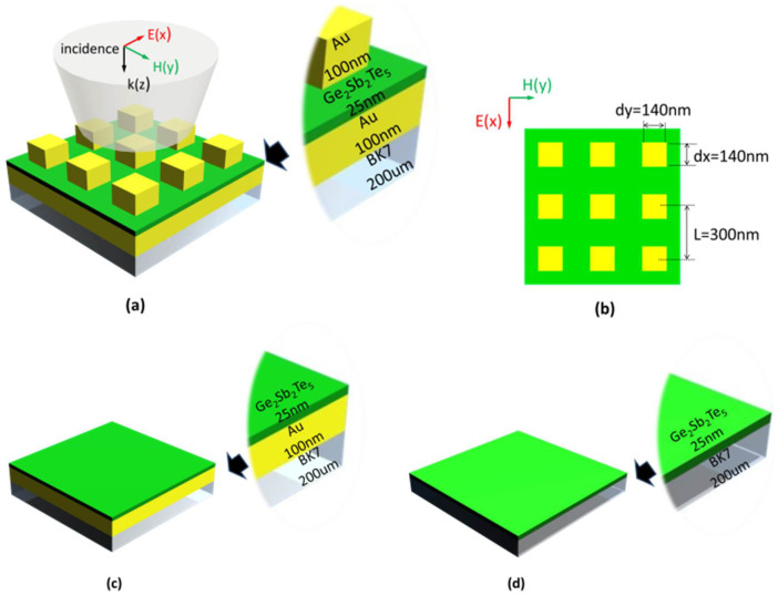
Our metamaterial absorber consists of two Au layers separated by a Ge2Sb2Te5 layer. Fig. 1(a)–(c) shows a schematic drawing of the tri-layer metamaterial absorber, where the lattice constant is L = 300 nm, the side length of the Au square is dx = dy = 140 nm, the thickness of the top Au layer is 100 nm, the Ge2Sb2Te5 layer is 25 nm and the bottom Au layer is 100 nm in order to prevent any transmission through the structure42. A single unit can be treated as an optical resonator. The unit cells are periodically arranged to form a two-dimensional square lattice in both the x and y directions. Furthermore, the thick Au bottom layer also interacts with the upper Au squares to give rise to a close loop of displacement current (JD) and localizes the electromagnetic (EM) field within the Ge2Sb2Te5 dielectric layer. The whole structure resides on a 200 μm thick BK7 glass. Au is selected as the metal due to its stability and low ohmic loss. The geometry of the Au pattern and the thickness of the sandwich layers that vitally affect the dipolar resonances have been chosen to allow for both impedance matching and strong absorbance, whilst the square shaped upper Au layer is expected to provide polarization independent excitation of the resonances43. For comparison, a 25 nm thick Ge2Sb2Te5 dielectric layer with 100 nm thick ground Au layer and a single 25 nm thick Ge2Sb2Te5 dielectric layer are also shown in Fig. 1(c) and (d) respectively. The simulation is performed by commercial software COMSOL, which is based on the Finite Element Method (FEM). The dielectric properties of Au as given by Johnson & Christy are used44. All the structures are excited by a source with a wavelength range from 420 to 1220 nm, propagating along the negative z direction with the E field polarized in the x direction as shown in Fig. 1(a). The light source has a repetition rate, fr = 25 kHz and pulse duration of 0.25 ns. The light fluence illuminating the sample from a single pulse is written as45
 |
where P0 = 0.03 mW is the total power of the injection light, r is the distance from the beam center, w = 10 μm is Gaussian beam waist. Scattering boundary conditions are applied in the z direction and periodic boundaries are used for a unit cell in the x-y plane. The frequency dependent reflectance R(ω) and transmittance T(ω) were abstained from the S-parameters in the simulation package and the absorbance, A(ω), was calculated as A(ω) = 1 − T(ω) − R(ω)9.
Figure 1.
(a)Schematic of the metamaterial absorber and the incident light polarization configuration. The thicknesses of Au squares, Ge2Sb2Te5 spacer and Au mirror are 100 nm, 25 nm and 100 nm, respectively. The lattice constant in both x and y-directions is L = 300 nm and square dimension is dx = dy = 140 nm. The whole structure resides on a BK7 silica glass with 200 μm thickness. (b) Top view of the absorber. (c) Schematic of a 25 nm thick Ge2Sb2Te5 dielectric layer with 100 nm thick ground Au layer deposited on a BK7 silica glass. (d) Schematic of the single Ge2Sb2Te5 dielectric layer deposited on a BK7 silica glass.
Optical properties of Ge2Sb2Te5
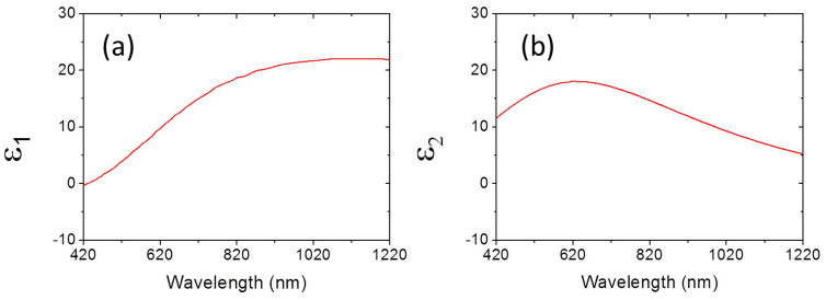
The real, ε1(ω) and imaginary, ε2(ω) parts of the dielectric function of Ge2Sb2Te5 in the amorphous phase are obtained from the experimental data in Ref. 29 and for the entire visible and near-infrared (NIR) spectral ranges the dielectric function is shown in Fig. 2. As can be seen, the dielectric constant of Ge2Sb2Te5 is very dispersive and has a large imaginary part indicating a high absorption coefficient. Thereby replacing the dielectric spacer with Ge2Sb2Te5 in MDM-MM absorber could enable broadband absorption.
Figure 2. Dielectric constant (a) ε1(ω) vs wavelength, (b) ε2(ω) vs wavelength for amorphous phase of Ge2Sb2Te5 [see reference 29].
Simulated optical properties of the broadband metamaterial perfect absorber
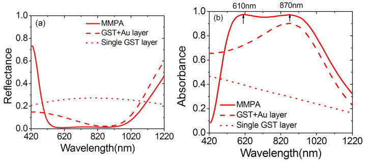
Firstly, we optimize the MMPA at normally incident TE (or TM) plane waves as shown in Fig. 1. The simulated reflectance R(ω) = |r|2 and absorbance A(ω) of the MMPA, an amorphous Ge2Sb2Te5 dielectric layer with ground Au layer, and monolithic Ge2Sb2Te5 dielectric layer at normal incidence are presented in Fig. 3, where r is the complex reflection coefficient. As can be seen, the MMPA possesses a low reflectance owing to impedance matching to the vacuum, leading to a strong absorbance over the entire visible region. However, the single amorphous Ge2Sb2Te5 film possesses the highest reflectance and lowest absorbance among the different structures due to the absence of the metal layers. In the MMPA, it is clear that a wide band near-perfect absorption around 670 nm is obtained with the absorbance of 96.8% at λ1 = 610 nm and 96.2% at λ2 = 870 nm. These two resonances are expected to account for this wide band near-perfect absorbance7,46.
Figure 3. 3D- FEM simulation of spectrum of (a) reflectance, (b) absorbance for the MMPA, Ge2Sb2Te5 dielectric layer with ground Au layer, and single Ge2Sb2Te5 dielectric layer at normal incidence.
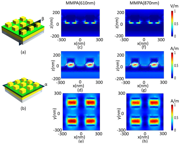
As stated previously, the top Au square array is responsible for electric dipolar resonances while the back Au layer is mainly used for creating magnetic dipolar resonances between the two metallic layers. Therefore, to gain insight on the localized surface plasmon resonance and the effect of Ge2Sb2Te5 in broadening the absorbance spectrum, we calculate the electromagnetic near-field distribution at normal incidence. Fig. 4 shows the field distributions and JD for the maximum absorbance of 0.968 at λ1 = 610 nm and 0.962 at λ2 = 870 nm for the MMPA. In the pattern, the white arrows represent JD whereas the color represents the magnitude of the electromagnetic field intensities.
Figure 4.
(a) Three dimensional schematic view of the MMPA showing the cross section plane β along x-z plane. (b) Three dimensional schematic view of the MMPA showing the cross section plane α along x-y plane at the top Au/bottom Ge2Sb2Te5 interface. (c) Total electric field intensity distribution along the β plane for the MMPA at λ1 = 610 nm. (d) The distributions of total magnetic field intensity distribution and displacement current (JD) along the β plane for the MMPA at λ1 = 610 nm. (e) Total magnetic field intensity distribution in α plane for the MMPA at λ1 = 610 nm. (f) Total electric field intensity distribution along the β plane for the MMPA at λ2 = 870 nm. (g) The distributions of total magnetic field intensity distribution and displacement current (JD) along the β plane for the MMPA at λ2 = 870 nm. (h) Total magnetic field intensity distribution in α plane for the MMPA at λ2 = 870 nm.
The total electric field intensity distribution associated with A(ω) = 0.968 at λ1 = 610 nm for the amorphous Ge2Sb2Te5 along a cross-section plane, β (as indicated in Fig. 4(a)) is shown in Fig. 4(c). It clearly shows that the electric field is mostly concentrated in the amorphous Ge2Sb2Te5 layer to excite the electric resonance moments. In Fig. 4(d), it shows that the total magnetic field intensity, along the β plane is also strongly localized in the amorphous Ge2Sb2Te5 dielectric layer. This is caused by the anti-parallel JD (shown as the white arrows in Fig. 4(d)) creating a loop between the Au square rods array and the bottom Au film17. These loops in JD give rise to artificial magnetic dipole moments that interact strongly with the incident magnetic field. Therefore, our structure provides a simultaneous excitation of electric and magnetic resonances to enhance the localized electromagnetic fields47. In Fig. 4(e), we depict the H field intensity in the interface plane of the top Au layer and Ge2Sb2Te5 dielectric layer, shown as the α plane in Fig. 4(b). It can be seen that the H field intensity is stronger in the centre of the unit cell indicating the strong magnetic dipolar moments formed between the Au square rods array and the bottom Au film5. In Figs. 4(f)–4(h), we show the total electric field, magnetic field, and JD, respectively, associated with A(ω) = 0.962 at λ2 = 870 nm. As can be seen, the field maps of the structure are similar with the ones at λ1 = 610 nm, which implies that the electrical resonant dipole and magnetic resonant dipole can also be simultaneously excited to create a strong absorbance.
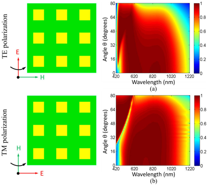
Ideally, the absorbance of the perfect absorber should be maintained at a large incidence angle and not depend on the light polarization5. Thus, Fig. 5 presents the absorbance as a function of wavelength and angle of incidence, where (a)–(b) show the absorbance for TE and TM polarization in the MMPA with an amorphous Ge2Sb2Te5 dielectric layer and the incident angle (θi) is varied in 1° steps from 0° to 80°. A broadband absorbance remains around 0.45 even at incident angle of 80° for TE polarization and 0.55 at 80° for TM polarization over the entire visible and NIR regimes. As can be seen, the increased θi results in an increment of absorbance below 450 nm, which is around the plasma frequency of bulk Au. With the higher angles of incidence, the path length of light in the nanostructures becomes longer, thus leading to a stronger absorbance of the light5. However, at longer wavelength, increasing θi leads to decreased absorbance. This is because the magnetic fields at large incident angles are confined less efficiently in the Ge2Sb2Te5 dielectric layer than at normal incidence, hence leading to a weaker magnetic dipolar resonance9 as shown in Fig. 6. In Fig. 5, note that there is a good spectral overlap between the absorbance for TE and TM polarizations. Thus, the proposed broadband MMPA is polarization-independent over a wide range of incident angles across the visible and NIR frequency regions.
Figure 5. 3D- FEM simulation of angular dispersions of the absorbance peaks (a) for amorphous Ge2Sb2Te5 at TE polarization, (b) for amorphous Ge2Sb2Te5 at TM polarization.
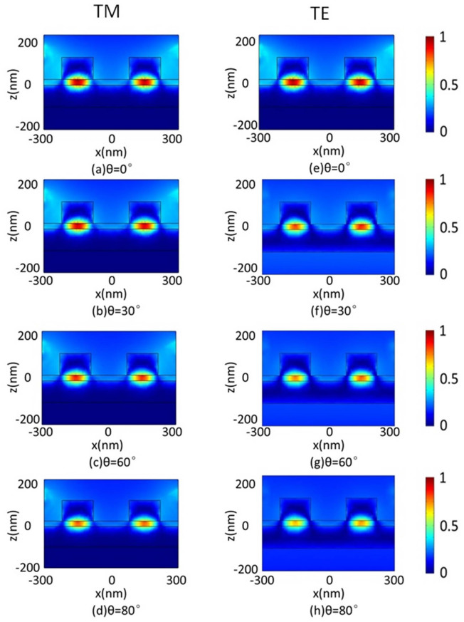
Figure 6. 3D-FEM simulation of total magnetic field distribution for TM polarization at (a) θ = 0°, (b) θ = 30°, (c) θ = 60°, (d) θ = 80°; For TE polarization at (e) θ = 0°, (f) θ = 30°, (g) θ = 60°, (h) θ = 80° where λ1 = 610 nm.
Further simulations were performed to study the relationship between the absorbance, the strength of the magnetic resonance at different oblique angles of the incidence. In Fig. 6, the total magnetic field intensity distributions at λ1 = 610 nm are investigated. It can be seen that the absorber maintains the localized magnetic field intensity thus the orientation of the magnetic resonant dipole at large incident angles. In particular, the localized magnetic field intensity for TM polarization shown in Fig. 6(a)–(d) is confined more strongly than for TE polarization shown in Fig. 6(e)–(h) at different incident angles. This is because the direction of the magnetic field of TM polarized light does not change significantly with incident angles and it can efficiently drive the current loop at all incident angles. Conversely, for the TE polarization, the magnetic field drives the circulating currents less efficiently at large angles48.
Fast phase transition of the Ge2Sb2Te5 in the metamaterial perfect absorber
The absorption of electromagnetic radiation in MMPA is mainly due to losses in the dielectric interlayer. Therefore Ge2Sb2Te5 is very promising and gives rise to a high and flat broadband absorbance due to its large imaginary part of the dielectric constant over the entire visible range. This strong absorbance allows rapid heating of the Ge2Sb2Te5 at visible wavelengths thus leading to a fast phase transition of the Ge2Sb2Te5 layer from the amorphous to crystalline state. To show this, a heat transfer model is used to investigate the temporal variation of temperature of Ge2Sb2Te5 layer for different structures using the Finite Element Method (FEM) solver within COMSOL. The material thermal properties used for the simulation are summarized in Table 1. The change in thermal conductivity of Ge2Sb2Te5 with the temperature is obtained from experimental data in Ref. 49. In this simulation, the thermal energy absorbed by one unit cell is defined as Ref. 45
 |
where L = 300 nm is the lattice constant of the metamaterials, Ra is 0.8952 for the MMPA, 0.7582 for the 25 nm thick Ge2Sb2Te5 dielectric layer with 100 nm thick ground Au layer, and 0.2797 for the monolithic 25 nm thick Ge2Sb2Te5 dielectric layer respectively. Ra is derived from the overlap integral between the light source power density spectrum and the absorbance spectrums of different structures, shown in Fig. 3(b), in the wavelength range from 420 nm to 1220 nm. The heat source power for different structures is then described by
 |
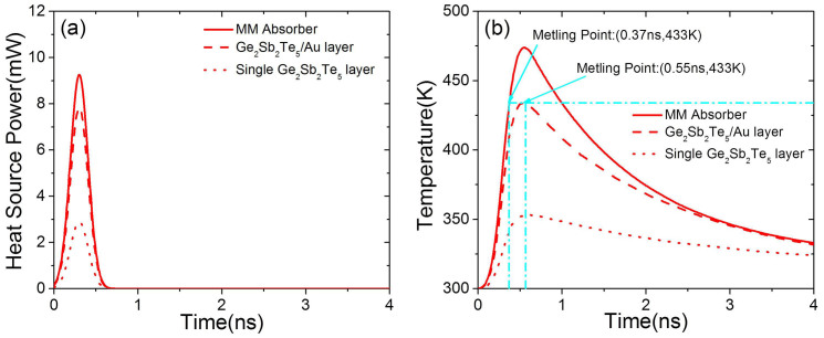
where τ = 0.15 ns is the time constant of the light pulse, t0 = 0.3 ns is the time delay of the pulse peak. Fig. 7(a) shows the heat source power: Qs(r,t) for the different structures, where the structures are located at the center of a Gaussian beam, and Fig. 7(b) shows the comparison of temperatures in Ge2Sb2Te5 dielectric layer for the three structures.
Table 1. Material thermal properties used in the Heat transfer model.
Figure 7. (a) 3D-FEM simulation of heat power irradiating on the MMPA (solid line), a 25 nm thick amorphous Ge2Sb2Te5 dielectric layer with 100 nm thick ground Au layer (dashed line), and 25 nm thick monolithic amorphous Ge2Sb2Te5 layer located at the beam center (dotted line), (b) Temperature during one pulse of amorphous Ge2Sb2Te5 layer in the MMPA (solid line), Ge2Sb2Te5 dielectric layer with ground Au layer (dashed line), single Ge2Sb2Te5 dielectric layer (dotted line).
In Fig. 7(b), the numerical simulation shows that the temperature within the amorphous Ge2Sb2Te5 dielectric layer of the MMPA is a function of the incident radiation flux and can exceed the amorphous to crystalline phase transition temperature of 433 K after 0.37 ns and a maximum of 474 K after 0.56 ns for a threshold incident flux of 95 nW/μm2. Due to heat dissipation and radiation to the surroundings, the MMPA begins to cool after 0.56 ns before the next pulse arrives. Eventually the temperature falls below the cubic crystal transition temperature. We have verified that a Ge2Sb2Te5 dielectric layer with ground Au layer can also reach the cubic crystallisation temperature of 433 K, but the time is 0.55 ns, nearly 0.18 ns longer than the MMPA. However, a bare film of Ge2Sb2Te5 cannot obtain 433 K under the same incident flux of 95 nW/μm2. A large temperature difference of 122 K at 0.56 ns between the MMPA and monolithic Ge2Sb2Te5 layer is clearly shown in Fig. 7(b); thus showing the usefulness of a metamaterial absorber for increasing the rate at which heat is delivered to Ge2Sb2Te5. Here, we do not consider the change in the optical properties during the phase transition of Ge2Sb2Te5. Here, we focus on showing that the MMPA decreases the time necessary to reach the amorphous to polycrystalline cubic phase transition temperature.
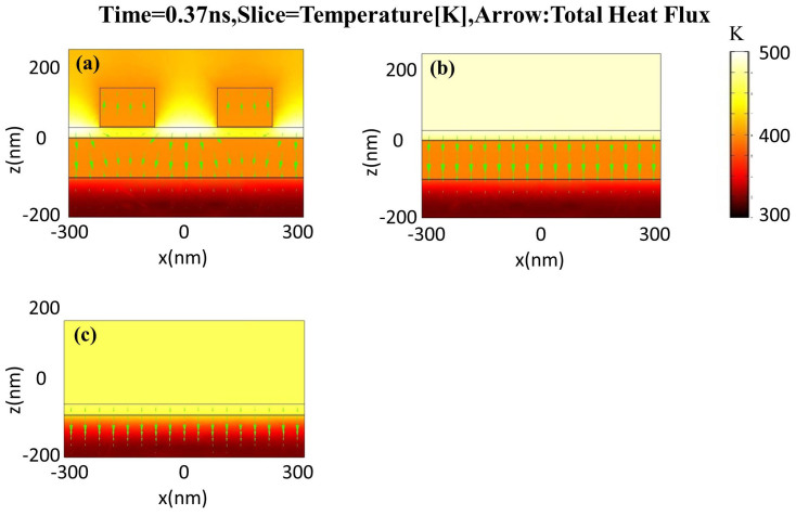
The temperature distribution of the structures at 0.37 ns is shown in Fig. 8(a), (b) and (c) respectively. One can observe that the temperature within amorphous Ge2Sb2Te5 dielectric layer of the MMPA is the highest. In all of the structures, the dominant temperature gradient is along the same direction as the incident light, indicating that BK7 silica substrate is an effective heat sink45.
Figure 8. The cross section view of the unit cell of the (a) MMPA, (b) Ge2Sb2Te5 layer with Au layer, (c) Monolithic Ge2Sb2Te5 layer, where the color indicates the temperature distribution and the arrows indicate the heat flux at 0.37 ns.
Discussion
In conclusion, we have presented a simple design of a MMPA that shows a polarization-independent near perfect broadband absorbance in the visible frequency regions due to the inclusion of a thin film of phase change material (Ge2Sb2Te5) that exhibits a large imaginary part of its dielectric constant. Total E and H intensity distributions have been presented to show that the electromagnetic field can be trapped efficiently inside the absorber over a wide range of incident angles. Furthermore, the absorbance spectra show substantial overlap between TE and TM polarizations. We have also studied the heat generation and temperature distribution within the structures, which triggers the amorphous to crystalline phase transition in Ge2Sb2Te5 for a low light intensity of 95 nW/μm2. In contrast, the time required to reach the amorphous to crystal phase transition temperature of the Ge2Sb2Te5 layer with a Au ground layer (0.55 ns) are longer than the Ge2Sb2Te5 layer in MMPA (0.37 ns) under the same conditions of optical illumination. Therefore, such a MMPA can be applied to achieve fast and energy efficient optical devices based on PCMs, and can find numerous applications in energy harvesting, biology and optical storage.
Methods
For the numerical calculations, we used the Finite Element Method by means of COMSOL Multiphysics. The unit cell of the phase-change metamaterial is shown in Fig. 1. The incident light is normal to the x-y plane with E field polarized in x direction. To account for the periodic nature of the metamaterial, the model boundary at  and
and  is set to condition of perfect electric conductor and perfect magnetic conductor, respectively for normal incidence and Floquet boundary condition for oblique incidence. Scattering boundary conditions are applied in the z direction. The optical constant of gold is taken from the data of Johnson and Christy44.The dielectric function of Ge2Sb2Te5 in different phases are obtained from the experimental data in29.
Author Contributions
T.C., M.J.C. and R.E.S. conceived the idea of using phase-changed material for decreasing the time necessary to reach the amorphous to cubic transition temperature of Ge2Sb2Te5. T.C. designed the metamaterial and performed numerical analysis. C.W.W. and L.Z. carried out the simulations and prepared the figures. T.C. supervised the research. T.C. and M.J.C. co-wrote the manuscript.
Acknowledgments
We acknowledge the financial support from National Natural Science Foundation of China (Grant No. 61172059, 51302026), Ph.D Programs Foundation of Ministry of Education of China (Grant No. 20110041120015), Postdoctoral Gathering Project of Liaoning Province (Grant No. 2011921008), and The Fundamental Research for the Central University(Grant No. DUT12JB01).
References
- Landy N. I. et al. Perfect metamaterial absorber. Phys. Rev. Lett. 100, 207402 (2008). [DOI] [PubMed] [Google Scholar]
- Atwater H. A. & Polman A. Plasmonics for improved photovoltaic devices. Nat. Mater. 9, 205–214 (2010). [DOI] [PubMed] [Google Scholar]
- Nagpal P., Lindquist N. C., Oh S. H. & Norris D. J. Ultra-Smooth Patterned Metals for Plasmonics and Metamaterials. Science 325, 594–597 (2009). [DOI] [PubMed] [Google Scholar]
- Halas N. J. et al. Plasmons in Strongly Coupled Nanostructures. Chem. Rev. 111, 3913–3961 (2011). [DOI] [PubMed] [Google Scholar]
- Aydin K., Ferry V. E., Briggs R. M. & Atwater H. A. Broadband polarization-independent resonant light absorption using ultrathin plasmonic super absorbers. Nat. Commun. 2, 517 (2011). [DOI] [PubMed] [Google Scholar]
- Tao H. et al. A metamaterial absorber for the terahertz regime: design, fabrication and characterization. Opt. Express 16, 7181–7188 (2008). [DOI] [PubMed] [Google Scholar]
- Avitzour Y., Urzhumov Y. A. & Shvets G. Wide-angle infrared absorber based on a negative-index plasmonic metamaterial. Phys. Rev. B 79, 045131 (2009). [Google Scholar]
- Liu X., Starr T., Starr A. F. & Padilla W. J. Infrared spatial and frequency selective metamaterial with near-unity absorbance. Phys. Rev. Lett. 104, 207403 (2010). [DOI] [PubMed] [Google Scholar]
- Liu N. et al. Infrared perfect absorber and its application as plasmonic sensor. Nano Lett. 10, 2342–2348 (2010). [DOI] [PubMed] [Google Scholar]
- Greffet J. J. et al. Coherent emission of light by thermal sources. Nature 416, 61–64 (2002). [DOI] [PubMed] [Google Scholar]
- Pala R. A. et al. Design of plasmonic thin-film solar cells with broadband absorption enhancements. Adv. Mater. 21, 3504–3509 (2009). [Google Scholar]
- Wen Q. Y. et al. Dual band terahertz metamaterial absorber: Design, fabrication, and characterization. Appl. Phys. Lett. 95, 241111 (2009). [Google Scholar]
- Tao H. et al. A dual band terahertz metamaterial absorber. J. Phys. D 43, 225102 (2010). [Google Scholar]
- Ma Y. et al. A terahertz polarization insensitive dual band metamaterial absorber. Opt. Lett. 36, 945–947 (2011). [DOI] [PubMed] [Google Scholar]
- Li H. et al. Ultrathin multiband gigahertz metamaterial absorbers. J. Appl. Phys. 110, 014909 (2011). [Google Scholar]
- Shen X. et al. Polarization-independent wide-angle triple-band metamaterial absorber. Opt. Express 19, 9401 (2011). [DOI] [PubMed] [Google Scholar]
- Cao T., Zhang L., Simpson R. E. & Cryan M. J. Mid-infrared tunable polarization-independent perfect absorber using a phase-change metamaterial. J.Opt.Soc.Am.B 30, 1580–1585 (2013). [Google Scholar]
- Hu C. et al. Mixed plasmons coupling for expanding the bandwidth of near-perfect absorption at visible frequencies. Opt. Express 17, 16745–16749 (2009). [DOI] [PubMed] [Google Scholar]
- Ye Y. Q., Jin Y. & He S. Omnidirectional, polarization-insensitive and broadband thin absorber in the terahertz regime. J. Opt. Soc. Am. B 27, 498–504 (2010). [Google Scholar]
- Wakatsuchi H., Greedy S., Christopoulos C. & Paul J. Customised broadband metamaterial absorbers for arbitrary polarization. Opt. Express 18, 22187–22198 (2010). [DOI] [PubMed] [Google Scholar]
- Luo H., Cheng Y. Z. & Gong R. Z. Numerical study of metamaterial absorber and extending absorbance bandwidth based on multi-square patches. Eur. Phys. J. B 81, 387–392 (2011). [Google Scholar]
- Alici K. B., Turhan A. B., Soukoulis C. M. & Ozbay E. Optically thin composite resonant absorber at the near-infrared band: a polarization independent and spectrally broadband configuration. Opt. Express 19, 14260 (2011). [DOI] [PubMed] [Google Scholar]
- Grant J. et al. Polarization insensitive, broadband terahertz metamaterial absorber. Opt. Lett. 36, 3476–3478 (2011). [DOI] [PubMed] [Google Scholar]
- Liu X. et al. Taming the Blackbody with Infrared Metamaterials as Selective Thermal Emitters. Phys. Rev. Lett. 107, 045901 (2011). [DOI] [PubMed] [Google Scholar]
- Huang L. et al. Experimental demonstration of terahertz metamaterial absorbers with a broad and flat high absorption band. Opt. Lett. 37, 154–156 (2012). [DOI] [PubMed] [Google Scholar]
- Lee H. M. & Wu J. C. Temperature Controlled Perfect Absorber Based on Metal-Superconductor-Metal Square Array. IEEE Trans. Magn. 48, 4243–4246 (2012). [Google Scholar]
- Hao J. et al. High performance optical absorber based on a plasmonic metamaterial. Appl. Phys. Lett. 96, 251104 (2010). [Google Scholar]
- Kats M. A. et al. Ultra-thin perfect absorber employing a tunable phase change material. Appl. Phys. Lett. 101, 221101 (2012). [Google Scholar]
- Shportko K. et al. Resonant bonding in crystalline phase-change materials. Nature 7, 653–658 (2008). [DOI] [PubMed] [Google Scholar]
- Michel A. U. et al. Using Low-Loss Phase-Change Materials for Mid-Infrared Antenna Resonance Tuning. Nano. Lett. 13, 3470–3475 (2013). [DOI] [PubMed] [Google Scholar]
- Orava J. et al. Optical properties and phase change transition in Ge2Sb2Te5 flash evaporated thin films studied by temperature dependent spectroscopic ellipsometry. J.Appl.Phys. 104, 043523 (2008). [Google Scholar]
- Orava J. et al. Characterization of supercooled liquid Ge2Sb2Te5 and its crystallization by ultra-fast-heating calorimetry. Nat. Mater. 11, 279–283 (2012). [DOI] [PubMed] [Google Scholar]
- Samson Z. L. et al. Metamaterial electro-optic switch of nanoscale thickness. Appl. Phys. Lett. 96, 143105 (2010). [Google Scholar]
- Yang Z., Ko C. & Ramanathan S. Oxide Electronics Utilizing Ultrafast Metal-Insulator Transitions. Annu. Rev. Mater. Res. 41, 337–367 (2011). [Google Scholar]
- Kats M. A. et al. Thermal tuning of mid-infrared plasmonic antenna arrays using a phase change material. Opt. Lett. 38, 368–370 (2013). [DOI] [PubMed] [Google Scholar]
- Dayal G. & Ramakrishna S. A. Metamaterial saturable absorber mirror. Opt. Lett. 38, 272–274 (2013). [DOI] [PubMed] [Google Scholar]
- Cao T., Simpson R. E. & Cryan M. J. Study of tunable negative index metamaterials based on phase-change materials. J. Opt. Soc. Am. B 30, 439–444 (2013). [Google Scholar]
- Wuttig M. & Salinga M. Phase Change Materials: Fast transformers. Nat. Mater. 11, 270–271 (2012). [DOI] [PubMed] [Google Scholar]
- Wang W. J. et al. Fast phase transitions induced by picosecond electrical pulses on phase change memory cells. Appl. Phys. Lett. 93, 043121 (2008). [Google Scholar]
- Bruns G. et al. Nanosecond switching in GeTe phase change memory cells. Appl. Phys. Lett. 95, 043108 (2009). [Google Scholar]
- Loke D. et al. Breaking the Speed Limits of Phase-Change Memory. Science 336, 1566 (2012). [DOI] [PubMed] [Google Scholar]
- Zhang B. et al. Polarization-independent dual-band infrared perfect absorber based on a metal-dielectric-metal elliptical nanodisk array. Opt. Express 19, 15221–15228 (2011). [DOI] [PubMed] [Google Scholar]
- Dayal G. & Ramakrishna S. A. Design of highly absorbing metamaterials for Infrared frequencies. Opt. Express 20, 17503–17508 (2012). [DOI] [PubMed] [Google Scholar]
- Johnson P. B. & Christy R. W. Optical constants of the noble metals. Phys. Rev. B 6, 4370–4379 (1972). [Google Scholar]
- Chen X., Chen Y., Yan M. & Qiu M. Nanosecond Photothermal Effects in Plasmonic Nanostructures. ACS Nano 6, 2550–2557 (2012). [DOI] [PubMed] [Google Scholar]
- Wang J. et al. Tunable broad-band perfect absorber by exciting of multiple plasmon resonances at optical frequency. Opt. Express 20, 14871–14878 (2012). [DOI] [PubMed] [Google Scholar]
- Lee H. M. & Wu J. C. A wide-angle dual-band infrared perfect absorber based on metal–dielectric–metal split square-ring and square array. J. Phys. D: Appl. Phys. 45, 205101 (2012). [Google Scholar]
- Tao H. et al. Highly flexible wide angle of incidence terahertz metamaterial absorber: Design, fabrication, and characterization. Phys. Rev. B 78, 241103 (2008). [Google Scholar]
- Kuwahara M. et al. Measurement of the thermal conductivity of nanometer scale thin films by thermoreflectance phenomenon. Microelectron. Eng. 84, 1792–1796 (2007). [Google Scholar]
- Chen G. & Hui P. Thermal conductivities of evaporated gold films on silicon and glass. Appl. Phys. Lett. 74, 2942 (1999). [Google Scholar]


