Abstract
Flip-chip packaging is desirable for microelectro-mechanical systems (MEMS) devices because it reduces the overall package size and allows scaling up the number of MEMS chips through 3-D stacks. In this report, we demonstrate three novel techniques to create first-level interconnect (FLI) on MEMS: 1) Dip and attach technology for Ag epoxy; 2) Dispense technology for solder paste; 3) Dispense, pull, and attach technology (DPAT) for solder paste. The above techniques required no additional microfabrication steps, produced no visible surface contamination on the MEMS active structures, and generated high-aspect-ratio interconnects. The developed FLIs were successfully tested on MEMS moveable microelectrodes microfabricated by SUMMiTVTM process producing no apparent detrimental effect due to outgassing. The bumping processes were successfully applied on Al-deposited bond pads of 100 μm × 100 μm with an average bump height of 101.3 μm for Ag and 184.8 μm for solder (63Sn, 37Pb). DPAT for solder paste produced bumps with the aspect ratio of 1.8 or more. The average shear strengths of Ag and solder bumps were 78 MPa and 689 kPa, respectively. The electrical test on Ag bumps at 794 A/cm2 demonstrated reliable electrical interconnects with negligible resistance. These scalable FLI technologies are potentially useful for MEMS flip-chip packaging and 3-D stacking.
Keywords: BioMEMS, flip chip, flux contamination, interconnects, microchip, packaging, solder, 3-D stacks
I. INTRODUCTION
PACKAGING of microelectromechanical systems (MEMS) devices or hybrid MEMS and integrated circuit (IC) are still mostly done by using wire bonding technique [1], [2]. Wire bonding may not be the preferable technique for MEMS packaging because: 1) it results in a much bigger package size than the actual die size; and 2) it provides no coverage for the MEMS active structures [3]—the wire interconnects are attached from the electrical pads on the die to the package with MEMS chip facing up, exposing the active part of MEMS. Recently, several encapsulation techniques [4]-[10] have been introduced to protect the active parts of inertial MEMS (such as accelerometers and gyroscopes) from harsh back-end packaging process such as wafer dicing, assembly, and wire bonding. Unfortunately, this encapsulation technique requires additional microfabrication steps to develop and attach a MEMS cap. Wire bonding also limits the ability to scale up [11] the number of MEMS devices—packaging more MEMS chips on the same substrate requires a significantly larger X-Y package form factor. In contrast, flip-chip packaging provides a number of advantages such as: 1) providing MEMS structures with a covering lid, which is the die/chip itself [12]; 2) opportunities to scale up the number of MEMS chips; and 3) integration of MEMS with others microchips (hybrid integration [1], [13], [14]), such as ASIC, microfluidics, and microgenerators, while maintaining the same X-Y form factor of the package through advanced 3-D stacking technology.
One of the key challenges in a flip-chip-based MEMS package is the first-level interconnect (FLI) that electrically connects the MEMS die and the substrate, such as printed circuit board (PCB), CMOS die, or glass substrates. Most commonly used FLI materials are Cu bumps/pads on the die with solder paste on the substrate [15] and Au/Cu pads on the die with solder spheres on the substrate [16], [17]. Pb-based solders with a melting point of approximately 185 °C [18] and Pb-free solders with a higher melting point of 235 °C [19] have been widely used in the semiconductor industries. Stencil printing to pattern the solder paste followed by a reflow process is one of the widely used techniques to create solder balls. These solder balls are then used for building the flip-chip interconnects between the substrate and the die for FLI or between the substrate to the PCB board to build the second-level interconnect. A variety of solder paste materials such as SnPb alloy, SnAgCu (SAC) alloy, and SnPbAg alloy can also be used. Alternative technology is a solder sphere/ball to create FLI. Nowadays, industries have used 100 μm solder sphere balls with flux to form the FLI. One simple procedure is to dip the solder spheres in a flux solution and then place them on the electrical pads followed by a reflow process. The flux causes the solder material to react with the electrical pads and make electrical bonds. Solder spheres with a minimum diameter of 100 μm are currently commercially available from Indium Inc. [20].
Unfortunately, the process of solder paste and solder spheres for IC cannot be applied directly to MEMS. One of the main reasons is the flux contamination [21], [22] on the MEMS chip. Flux is needed for solder paste or solder spheres as it activates the surface of the solder to react and wet other metals such as Cu and Au, to form alloy joint. Flux also reduces the surface oxidation on the metal surface. For IC packaging process, flux contamination is tolerable as it can be cleaned by a “deflux” process, where a jet of warm soapy water is impinged on the package to rinse the flux residue. However, in the case of MEMS chips, flux residue or contamination is a critical issue [23] as it directly impacts the functionality of MEMS active parts [22], and a conventional “deflux” process will be catastrophic for the mechanical microstructures.
To mitigate this flux contamination issue, solder paste suppliers (such as Indium Inc.) have introduced water cleanable flux and fluxless solder pastes. For water cleanable flux-based solder paste, the flux residue can be removed by deionized (DI) water or isoprophyl alcohol solution. This process has been successfully reported by [24] for packaging a MEMS pressure sensor. For many MEMS structures which contain complex active/moveable mechanical parts, DI water contamination is still not acceptable due to possible stiction issues [25], [26] which will reduce or completely impede the MEMS performance. For fluxless solder paste, the amount of flux composition is less than the commonly used solder paste. The flux residue is benign and usually remains on the base of solder ball after reflow. Cabruja et al. have successfully demonstrated in using a fluxless solder paste for packaging MEMS pressure sensors [27] by providing a good clearance distance (approximately 500 μm) between the solder bump and the MEMS active structures. For this design, most solder pads were located on the die’s perimeter [28] similar to a wire bonding arrangement, which results in a larger die size. Stark and Najafi have demonstrated a mold and transfer technique to create lead-free fluxless soldering by using mold developed by bulk micromachining on a silicon wafer [29]. Furthermore, solder paste does not wet or adhere well to metals such as Al or Cr. Most solder paste applications therefore use Au or Cu [30]. This further limits the use of solder paste in MEMS application.
Over the past two decades, there have been numerous efforts to develop novel interconnect technologies to realize flip chip for MEMS without the use of flux. Miller et al. [31] created a microrelay by soldering eutectic tin/lead bumps to gold in a formic acid environment. Wei Lin and Y. C. Lee used formic acid vapor for fluxless soldering with eutectic Pb/Sn solder [32]. Heschel et al. [33] generated 15 μm high eutectic SnAg 3.5 bumps by e-beam evaporation followed by an in situ reflow soldering in an ambience of reduced O2 which provides the benefit of self-alignment of the structures. Singh et al. [34] implemented a chrome-copper seed layer with 5.8 μm thick electroplated copper pads on the MEMS die and 15 μm high, 50 μm diameter indium bumps on the target die. To enable soldering without flux, both dies were cleaned in hydrochloric acid before the dies were aligned and joined. Applying the pressure at ambient temperature created a cold weld, and a reflow process at 170 °C was also possible. Another method for removing oxide from the surface to be soldered was plasma cleaning. The procedure used by Tilmans et al. [35] was named PADS. Oxides on tin-containing solders were converted to oxyflourides and thereby passivated. A Si substrate carrying the MEMS structure was then joined to the ferroelectric FeSi substrate by soldering electroplated SnPb to Au. The end product, a microrelay was packaged in a simple plastic surface mount component. All of the above examples in this paragraph required additional processes for the MEMS microfabrication. Therefore, the packaging issues must be well thought out before the design of the MEMS device. The packaging process for MEMS therefore became more customized for each specific MEMS device and required an extensive engineering development time.
Matsuhita used a stud bump bonding (SBB) [36] technique, where a microchip designed for wire bonding was bumped by using ball wire bonders (the gold was automatically pulled off after the ball bond was formed). The resulting bump had the shape of an upside down mushroom, and it was joined to the substrate using adhesives, or thermo compression, or soldering with gold alloys, and recently with ultrasonic bonding [37]. SBB provided a lot of flexibility. Bumps could be applied in any pattern, and no wafers masked were required. Pai and Walsh [3] used anisotropic conductive film and Au stud bumping to form interconnects between die and substrates with the potential applications to MEMS pressure sensors. Pai and Walsh used additional coining process after the stud bumping to reduce bump height variation. As a result, the final bump size became wider in diameter (155.5 μm) and shorter in height (32.98 μm). The drawback of the Au stud bumping process is that it only adhered to limited number of metals such as Au or Cu.
Oh et al. introduced a conductive polymer bumps with a height of 15 μm [38], [39] to bond MEMS die to a substrate. Recently, Li et al. used this technique to bond MEMS pressure sensors on a flexible Kapton film for neonatal catheters [40] application. The advantage of the conductive polymers compared with traditional solder flip-chip bonding was a lower process temperature (170 °C). However, this technique required additional steps on the substrate or on the die to pattern the polymer bumps by spin coating followed by lift-off process. The reported bonding strength between the polymer bumps and the substrate was 4.43 kPa, which is relatively low compared with the IC standard solder bump with the shear strength of 39–41 MPa [41], [42] at room temperature.
There have also been several attempts to batch transfer some parts of MEMS structures through flip-chip technology. In this process, some parts of MEMS structures were fabricated on a separate die/substrate, named as a donor die/substrate. Irwin et al. [43] presented a method of transferring MEMS structures to a host substrate using SBB. 100 μm diameter Au bumps were placed on the interconnect pads, the stud bumps were flattened, and the MEMS die was thermosonically bonded to the host substrate. The MEMS structures were then released with HF etching, and the host substrate remained. A drawback of the method was the increased time required in the etch bath due to the narrow gap. This caused an uncertainty in the etch stop, which might cause some damage to the transferred MEMS structures. Furthermore, since thermosonic bonding was used, alignment of the patterns must be very precise compared to when the solder was used [12]. The SBB technology in combination with thermosonic bonding was also used in a micro-mirror assembly [44]. Recently, Basavanhally et al. reported similar work in the batch transfer of the MEMS structure, where he demonstrated the patterning of high-density solder bump interconnects for MEMS hybrid integration [13]. The indium solder was evaporated on the channels patterned via photoresist, 3 μm diameter and 2.5 μm height, which acted as a mask. The photoresist mask was then lifted off leaving indium bumps on 5 μm pitch and diameter of 3 μm. The flip-chip bonding between the host die, which contained the CMOS ASIC, and the donor die, which contained the unreleased MEMS micromirror, was completed during one step of reflow process at temperatures of 200–220 °C with a load varying from 200 to 400 g for a period of 60 s. A special customized fixture was required to individually release the MEMS mirror. The customization of the process was very critical in this technology. The fabrication of interconnects required additional delicate processes in the MEMS fabrication. The release process of the MEMS structure also required a special treatment and customized apparatus.
Therefore, for the successful application of flip-chip technology for MEMS packaging, there is still a significant need for an interconnect technology that: 1) is simple to be applied to the MEMS chip after the MEMS fabrication process is completed and the patterning of interconnects does not require any additional microfabrication steps; 2) does not interfere or contaminate the MEMS active part during the development of the interconnects; 3) is robust and reliable in terms of a) bonding stress to meet the solder paste standard of the IC manufacturing process and b) low contact resistance between the two bonding pads; 4) flexible in the sense that it can be applied to bond any metal pads to any MEMS structures; the process must also be scalable for large arrays of interconnects; 5) adjustable height, the fabrication process of the interconnects can be tailored to meet the required height depending on its application. This study reports techniques to develop FLI structures by using Ag epoxy and solder paste. We have developed these techniques by using Ag epoxy and solder paste material because Ag is well-known for its high electrical conductivity, and solder paste is a commonly used to build bumps in the semiconductors industries. These techniques can be potentially used for other interconnect materials as well. However, the following recipes described in this report are optimized for Ag epoxy and solder paste materials.
Dip and attach technique (DAT) for Ag epoxy interconnect.
Dispense technique (DT) for solder paste interconnect.
Dispense, pull, and attach technique (DPAT) for solder paste interconnect.
These techniques require no additional microfabrication process, produce no apparent surface contamination, are robust, flexible, and can be used to create high-aspect-ratio interconnect bumps. These three technologies to develop novel interconnects can be used as the building platform for MEMS flip-chip technology. This report will demonstrate the success of the technologies in making FLIs using Ag epoxy and solder paste.
II. METHODS
A. Dispensing Technology
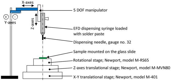
In this section, a simple and economical nozzle dispensing technique to create bumps for the FLIs is described. This process was carried out by using our custom-made flip-chip setup station shown in Fig. 1. Unlike currently available methods which typically required separate equipment for each packaging step, the setup shown in Fig. 1 was capable of dispensing solder paste, performing reflow, flip chip, and finally underfill for semi-hermetic encapsulation. While the report here is focused on the techniques for creating novel FLI, the process reported here is scalable to create 3-D-stacks of MEMS chips.
Fig. 1.
Illustration of the custom-made setup for flip-chip interconnect.
1) Dip and Attach Technique (DAT) for Ag Epoxy Interconnect
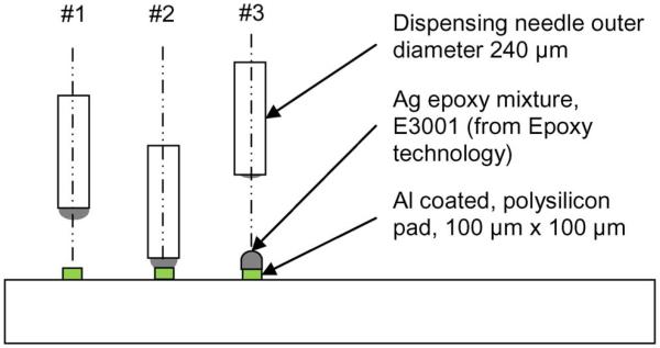
The schematic of steps involved in the development of interconnects using Ag epoxy bumps is shown in Fig. 2. In this technique, commercially available Ag epoxy (E3001, Epoxy Technology Inc., Billerica, MA) was used. Ag epoxy contained Ag particulates 1–5 μm in diameter. The process to create a single bump on a 100 μm × 100 μm pad involved three simple steps: 1) dip the dispensing needle with the outer diameter of 240 μm into a bath of Ag epoxy until the tip of the needle was fully covered by Ag epoxy. Retrieve the needle with a small amount of Ag epoxy on its tip; 2) bring the needle closer to the pad until the Ag epoxy fully touched and covered the bond pad; 3) retrieve the needle with a small amount of Ag epoxy residue on its tip. Most of the Ag epoxy was attached to the bond pad forming a bump.
Fig. 2.
Schematic of the steps involved in the development of Ag bump interconnects through Dip and Attach technique (DAT).
2) Dispense Technique (DT) for Solder Paste Interconnect
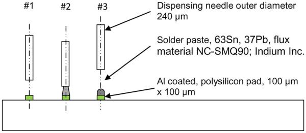
The DT of solder paste from a nozzle with the inner diameter of 100 μm can be described by the schematic shown in Fig. 3. In this technique, commercially available Pb-based solder paste (63Sn, 37Pb, flux material NC-SMQ90) from Indium Inc. was used with the mesh type 6, which contains 5–15 μm diameter solder particulates. A pneumatic dispenser (Ultimus I, Electronic fluid dispensing, Nordson Inc., Westlake, OH) with precision stainless steel dispensing tips (32 gauge) having an inner diameter of 100 μm was used.
Fig. 3.
Schematic of the steps involved in the development of solder bump interconnects through “dispense technique (DT).”
The process to create a single bump on a 100 μm × 100 μm pad required three steps: 1) the dispensing needle was brought into a close proximity (25–50 μm) with the pad’s surface, which could be a bond pad or a die surface with underlying interconnects. Since the needle inner diameter was approximately 100 μm, the distance between the needle and the bond pad should not exceed 100 μm at the time of dispensing; 2) Solder paste was dispensed. The size of the pad dictated the amount of solder paste to be dispensed. In this report, for a pad size of 100 μm × 100 μm square, the solder paste was dispensed with a pressure of 60 psi and a pulse time of 10 ms with two pulses/puffs; 3) the dispensing needle was then pulled away from the die surface. Additional solder paste can be added by continuing steps #2 and #3 to create bumps of higher aspect ratio. We have made solder paste bumps with heights of 80–90 μm after reflow, after multiple dispensing steps.
The solder paste shape is determined by forces of surface tension and adhesion between the flux and the bond pad. Larger than optimal quantity of solder paste may however cause overflow and potential contamination beyond the pad boundary.
3) Dispense, Pull, and Attach Technique (DPAT) for Solder Paste Interconnect
The dispense, pull, and attach technique (DPAT) of solder paste from a nozzle with the inner diameter of 100 μm can be described by the schematic pictures shown in Fig. 4. The processes to create a single bump on a 100 μm × 100 μm pad required six simple steps: 1) a place/region which was not the place where the solder will be finally dispensed was chosen; 2) a needle is brought in close proximity to the surface (approximately 25 μm) and the first pulse or puff is delivered to dispense the solder paste; 3) the needle is slowly retrieved upward while continuing to dispense the solder paste for the second, third, fourth puffs, etc., until the solder paste started to neck; 4) Once the needle was fully retrieved, a long rod-shaped structure of solder paste was produced. This shape was produced by forces of surface tension and adhesion between the flux and the needle’s orifice; 5) The solder paste was brought in contact with the surface of solder pad, and the needle retrieved slowly; 6) A tall bump was produced. For a 100 μm electrical bond pads, bumps as tall as 250 to 300 μm can be produced prior to reflow.
Fig. 4.

Schematic of the steps involved in the development of solder bump interconnects through “dispense, pull, and attach technique (DPAT)”.
B. Reflow Process for Solder Paste Bumps
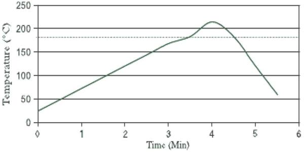
There was no reflow process for the Ag epoxy interconnects. The Ag epoxy after the “dip and attach” process was fully cured at a temperature of 120 °C for 60 s. Reflow process is needed for solder paste, and it is a critical process in the development of flip-chip interconnects. During the reflow process, a number of things happen: 1) flux and solder separate; 2) solder particulates merge together overcoming the surface tension that separates flux and solder particulates; 3) solder particulates merge with one another and make surface contacts; 4) flux evaporates. The solder reflow process recommended by the manufacturer is shown in Fig. 5. It is a fast and volatile process, which typically lasts for 3–5 min, rising to a temperature 30 °C to 40 °C above the melting temperature of solder. During this reflow process, the flux is still wet as it does not have sufficient time to fully evaporate. The flux reacts chemically with the solder particulates and forms a smooth spherical solder bump. Any excess flux will be left underneath the solder sphere as a yellow solidified residue. In the semiconductor industry, this excess flux is typically removed by a jet of warm water and soap solution. This flux removal process is nonideal for microchips with moveable mechanical structures. The fast reflow process will therefore contaminate the area surrounding the bond pads in a MEMS chip which can jam/freeze the active mechanical structures.
Fig. 5.
Normal solder reflow process, adapted from Indium Inc. for 63Sn 37Pb solder paste.
1) Slow Reflow Process
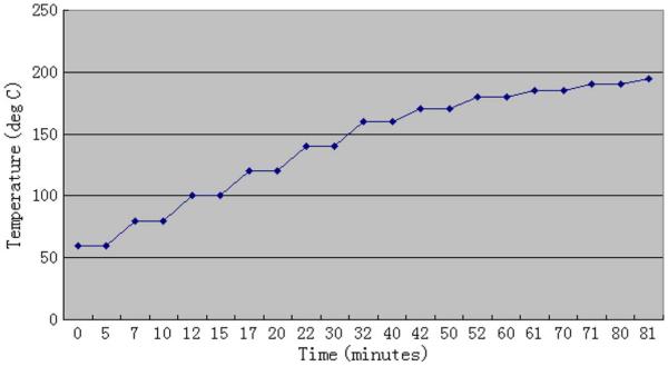
A new optimal slow reflow process, which ramped up to the melting point of solder (185 °C) over a period of 60–80 mins was developed for this study to create solder bumps without apparent surface contamination. The new reflow process as shown in Fig. 6 allowed sufficient time for the flux to fully evaporate during the reflow time; it also provided adequate time for the solder particulates to merge and melt. Visual observations under the microscope and SEM showed that there was no spillover of flux or contamination around the solder bump, making it safe for active MEMS mechanical structures. A very thin layer of flux approximately 20–50 μm from the bump boundaries may be observed. Therefore, the bond pads can now be brought close to the active MEMS structure. Due to the slow nature of the reflow process, the outer shape of solder bump revealed the grain boundary of the solder particulate at the end of the reflow. This rough grain boundary may lead to possible pin fracture if an indentation force was applied to the bump. However, force to the solder joint is typically a shear force, and it is not a point force. It is noted that the shape of the solder bump after reflow was not significantly different from the shape before reflow. This observation can possibly be useful for other future applications.
Fig. 6.
Temperature profile during the optimal slow reflow process for creating solder bumps.
C. Bump Strength Characterization
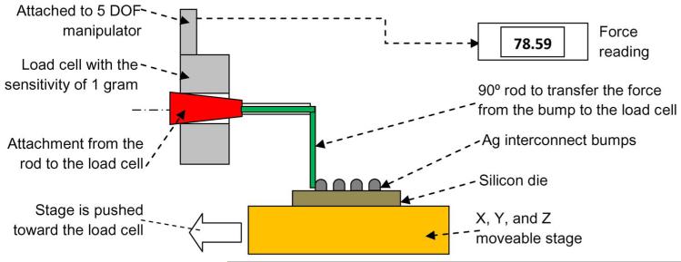
To measure the mechanical strength of Ag interconnect bumps, the bumps were subjected to increasing shear forces until they failed. A custom made setup with a 1-g load cell (OmegaDyne, Sunbury, Ohio), shown in Fig. 7, was used to perform this characterization. As shown in Fig. 7, the bump strength characterization was carried out by pushing the Ag epoxy toward the rigid 90° rod, which transferred force along the x-axes to the load cell. The load cell was connected to a digital readout which recorded the maximum force experienced by the bump before it failed. To obtain maximal shear force, the tip of the rod was brought closer to the bump’s base. The shear stress was calculated by dividing the reading force with 100 μm × 100 μm pad area. A mechanical stress test was also conducted on a silicon die with eight Ag interconnect bumps after being flip chipped on a glass substrate. The schematic of the test is shown Fig. 8. After the flip-chip process is completed, axial force is applied on the glass. This force creates combined shear and bending stresses on the Ag interconnect joints.
Fig. 7.
Schematic of the setup for shear stress characterization of Ag interconnect bumps.
Fig. 8.

Schematic of the setup for mechanical strength test of the Ag interconnect bumps after the flip-chip assembly on a glass substrate.
As mentioned earlier, the surface of the solder bumps has grain boundaries of the solder particulates, which can be a potential weak spot for pin-point force. To measure the mechanical strength of the solder bumps, an alternative method to avoid contact with the bumps was used. Pressurized air from a nozzle (100 μm inner diameter) was brought in close proximity to the bumps to provide axial/shear impinging air pressure to the bumps. A solder dispensing station (EFD Ultimus I, Nordson Inc.) was used as the air-jet controller.
D. Test of Electrical Functionality
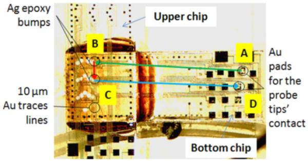
To measure the electrical interconnect capabilities of the Ag bumps, two glass chips with patterns of thermally deposited Au trace lines at a thickness of 1500 Å were utilized. Each glass chip consists of Au bonding pads each with a size of 500 μm × 500 μm, on the one end of the chip as shown in Fig. 9 (labeled as “bottom chip” in the figure). These pads were used for probe tip contacts. In addition, 15 Au bond pads of 100 μm × 100 μm were located on the left end of the chip as shown in Fig. 9. Ag bumps (n = 15) were created on these 15 Au bond pads.
Fig. 9.
Flip-chip configuration for electrical test of the Ag interconnect bumps.
Three Ag bumps (two of which were named B and C as in Fig. 9) on the bottom chip were aligned to the 10 μm trace lines on the upper chip. The upper chip was then flip chipped on the bottom chip followed by the underfill process using electronic epoxy as shown in Fig. 9. The Au trace lines on the upper chip were used as electrical connection between bump B and bump C. Pads A and D were used for making contact with the probe tips. Voltage is applied across pads A and D while simultaneously measuring current. Five different voltages were applied ranging from 1 V to 5 V in 1 V increments. For each voltage, the current was measured continuously for over 3 h under room conditions.
III. RESULTS
A. Bump Interconnects and Height Characterization
Micrographs and SEM images were used to calculate the height of the bump interconnects after curing (for Ag epoxy) and reflow (for solder paste) process.
1) Ag Bumps Interconnects
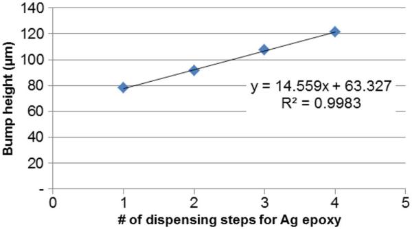
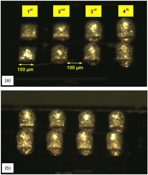
For Ag bump interconnects, taller bumps were achieved by simply repeating the “dip and attach” steps described in Fig. 3. The measured bump height from the base of the pad to the top of the bump as a function of the number of dispensing steps is shown in Fig. 10 demonstrating a linear trend. For a single “dip and attach (DAT)” step, the bump’s height after reflow was approximately 80 μm. Bump as tall as 120 μm can be produced after four DAT steps. The ability to create consistent bumps of different heights is advantageous as different applications may require different bump heights, e.g., CPUs typically require a bump height of 50 μm, while MEMS applications may require bump heights of 100 μm. A shorter bump height can be achieved by having smaller pad size of 50 μm × 50 μm, and bumps as short as 30 μm can be achieved with one single step of DAT. Smaller bump pads will provide more space for higher density interconnects (HDIs) (Fig. 11).
Fig. 10.
Bump height versus the number of Ag epoxy dispensing steps.
Fig. 11.
Micrographs (a) Ag epoxy bumps of increasing heights after successive dispensing steps and (b) showing the Ag epoxy bumps after four dispensing steps.
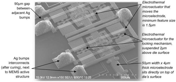
The DAT process was also applied on a MEMS device— a highly sensitive MEMS moveable microactuator fabricated using the SUMMiTVTM process in Sandia National Laboratories, NM. The MEMS active structure is electrothermally actuated with the minimum feature size of less than 1.5 μm. The microelectrode with the width of 50 μm and the thickness of 4 μm sits directly on the die’s surface and moves along the “in-plane (X-axes)” direction. A thin layer of surface contamination on the path of microelectrode moveable can potentially jam/freeze the microelectrode’s movement. A solid particulate contamination in or on the MEMS active structure would impede, hinder, or choke the electrothermal microstructures, which are suspended 2 μm above the die’s surface. The MEMS electrothermal actuator was used to drive the micro-electrode into the brain tissue for single neuronal recordings from rodents. The operation and functionality of these MEMS microelectrodes are described in [45], [46].
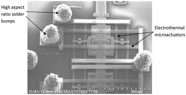
An SEM image of the MEMS electrothermal actuator—with Ag interconnect bumps built on top of Al coated pads—is shown in Fig. 12. Three steps of dispensing on each pad created Ag interconnect bumps (n = 18) with an average height of 101.3 μm, as described in Table I. Each MEMS electrothermal actuator contained six Al deposited bumps pads with the dimensions of 100 μm × 100 μm. The smallest distance between adjacent pads was 90 μm. These pads were initially designed for Al wire bonding application. There were a total of eighteen MEMS actuators on a die, with the overall dimension of 2.8 mm × 6.3 mm and a total of 18 bumps.
Fig. 12.
MEMS actuator with Ag bumps interconnects.
TABLE I.
Height Statistics of 18 Ag Epoxy Bumps on a MEMS Chip
| Average = | 101.3 μm |
| standard Deviation = | 3.13 μm |
| Max = | 107 μm |
| Min = | 97 μm |
| Range = | 10 μm |
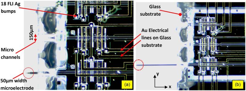
As shown in Fig. 12, the bond pads were built close to the active MEMS structures with a distance of less than 25 μm from the pad boundary to the electrothermal heating strips that move under electrical activation. This small distance obviously creates a great challenge for the bumping process as any contamination during the bumps application process will freeze the MEMS active parts. There was no visible surface contamination of the active MEMS structures (as shown in Fig. 12) after three steps of “dip and attach” process of Ag epoxy followed by curing. The MEMS devices were tested before (by using a probe station) and after the bumping process (the MEMS die is fully flip chipped on a glass substrate with Omnetics interconnects). The static (one increment step movement at 8.8 μm/step) and dynamic (moved at 10 Hz frequency with the maximum stroke of 5 mm) results show that the possible outgassing that occurs during the flip-chip packaging processes (including the curing process of the Ag bumps) create no apparent detrimental effect on the MEMS functionality. The position of one of the microelectrodes in a fully packaged flip-chip MEMS microactuator before and after the actuation using the electrothermal actuators on the die is shown in Fig. 13. Fig. 13(b) shows that the electrode has moved approximately 2 mm.
Fig. 13.
Fully packaged MEMS die (2.8 mm × 3.6 mm) flip chipped on a glass substrate. Ag bumps were used as the FLIs. (a): the bottom MEMS microelectrode, prior to actuation; (b): Bottom MEMS microelectrode after 2-mm actuation.
Details of the packaging steps to create fully packaged MEMS flip chip and the technique to create semihermetic seal microchannels as shown in Fig. 13 will be presented in an accompanying manuscript. This report is focused only on the novel technology to develop FLI, which is critical to the development of a fully packaged MEMS device through flip-chip technology.
2) Solder Bump Interconnects
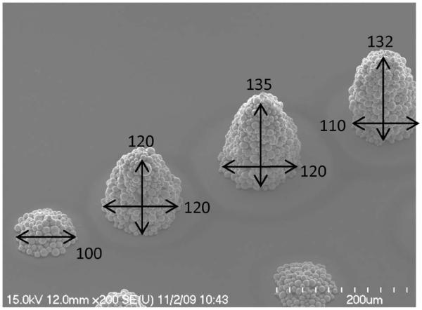
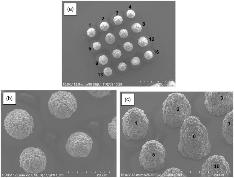
Solder bumps made using DT are shown in Fig. 14. The solder paste was dispensed on Cr (about 0.1 μm thick) deposited pads with the size of 100 μm × 100 μm and a 100 μm distance between pads. As shown in Fig. 14, there was no visible surface contamination on the silicon surface. There was a very thin residue approximately 25 μm surrounding the outer boundary of the bump’s base. It is likely that this residue came from the flux solution. Therefore, any active MEMS structures can be placed at a distance of at least 50 μm from the solder bumps. Solder bumps made using the DPAT are shown in Fig. 15. The solder paste is dispensed on a 4 × 4 array of Cr-deposited pads each with the size of 100 μm × 100 μm and a gap distance of 100 μm. Table II shows the summary of the bump’s base diameter, bump height, and aspect ratio for arrays of 16 bumps. As summarized in Table II, the resulting bumps had an average base diameter of 115.5 μm, an average height of 189.7 μm, and an average aspect ratio of 1.64. As shown in Fig. 15, there was no visible contamination on the silicon surface surrounding the bumps. There was a very thin residue about 30 to 40 μm from the outer boundary of the bump’s base, which was consistent to the results for DT. This result also suggests that there was sufficient time for the flux to fully evaporate while the solder particulates slowly merged and bound together during the optimal slow reflow process.
Fig. 14.
SEM image of solder bumps made using “dispense technique” (DT).
Fig. 15.
(a)–(c). SEM images of solder bumps made by “dispense, pull, and attach technique” (DPAT).
TABLE II.
Geometrical Summary of 4 × 4 Arrays of DPAT Solder Bumps
| Diameter | Average = | 115.5 μm |
| Standard Dev = | 6.46 μm | |
| Max = | 125 μm | |
| Min = | 105 μm | |
| Height | Average = | 189.7 μm |
| Standard Dev = | 7.07 μm | |
| Max = | 200 μm | |
| Min = | 180 μm | |
| Aspect Ratio | Average = | 1.64 |
| Max = | 1.74 | |
| Min = | 1.51 |
As shown in Fig. 15, the solder particulates were bonded to one another to form pillars. However, bumps #6 and #8 appeared to be defective due to flux being trapped among the solder particulates. These defects were validated first by a visual inspection under the microscope which showed solidified flux in between the solder particulates. Subsequently, a destructive shear test exposing a cross section of the bump showed flux in between the solder particulates, particularly near the outer perimeter of the bump. It was possible that for bumps # 6 and #8, the dispensed solder paste had more flux than for the rest of the bumps. This flux did not get chance to evaporate fully during the reflow process and likely got solidified when brought back into a room temperature.
The DPAT technology was also tested on the MEMS move-able microelectrode fabricated using SUMMiTVTM process in Sandia National Laboratories, NM. An SEM image of the MEMS active microstructure with solder interconnect bumps (created by DPAT) built on top of the Al coated pads is shown in Fig. 16. Because Al did not adhere well with solder, a thin layer of Ag epoxy was applied to Al pads prior to DPAT process. Fig. 16 shows no visible thin film of flux residue on the die surface surrounding the bumps unlike the results shown in Figs. 14 and 15. Flux residue, in this case, was eliminated by having a tall (approximately 12 μm) Al-coated polysilicon pad, which prevented the flux residue from leaking beyond the pad boundary. Fig. 16 shows that the MEMS active structures close to the bumps remain uncontaminated and undisturbed. The statistics of the 18 bumps of DPAT solder interconnect are summarized in Table III. The average height of the solder interconnects is 184.8 μm. The heights of the DPAT bumps are uniform with a tolerance of 14%.
Fig. 16.
MEMS actuator with DPAT solder bumps interconnects, aspect ratio of 1.85 average.
TABLE III.
Height Statistics of 18 DPAT Solder Bumps on a MEMS Chip
| Average = | 184.8 μm |
| standard Deviation = | 13.6 μm |
| Max = | 195 μm |
| MIN = | 167 μm |
| Range = | 28 μm |
3) Standard Solder Reflow
Fig. 17(a) shows the picture of high-aspect-ratio solder pastes applied on four Al pads by using the DPAT process. Before the reflow process, the bump height is approximately 240 μm, while the pad size is 100 μm. After the standard reflow process, which is normally used by IC (as shown in Fig. 5), the final bump size is 140 μm in diameter with the height of 135 μm. The shape of the bump is almost spherical. Unlike the slow reflow process that produces the final bump size with the aspect ratio >1 as shown in Fig. 16, standard reflow process produces solder bumps with the aspect ratio of 0.96, as shown in Fig. 17(b). Therefore, the bump height is normally shorter than the diameter for normal reflow process.
Fig. 17.
(a) Four bumps are formed on Al pad by using DPAT process; the average height is approximately 240 μm—before the reflow process. (b) The four bumps after the standard reflow process, the average height is 135 μm; the flux residue is solidified at the base of the bumps. Bump shape is almost spherical.
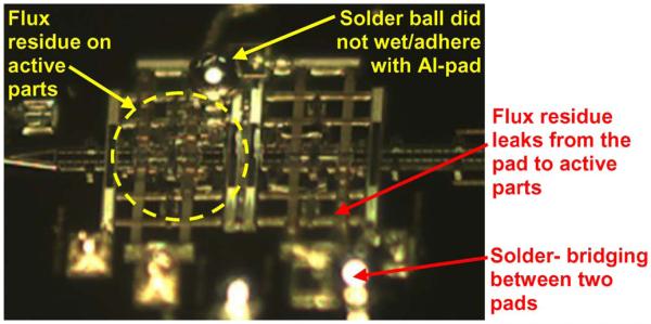
Fig. 17(b) shows that most flux residue is solidified at the base of the bump. This flux residue frequently leaks from the bonding pad onto the MEMS active part as shown in Fig. 18 and causes severe contamination and freezes the MEMS electro-mechanical structures. Because solder ball did not wet or adhere well with Al, solder bumps are often shifted during the reflow process (as in Fig. 18), which caused further contamination on MEMS structures. As mentioned before, reflow is a volatile process, and solder bridging may occur when the pads are too close to one another. Fig. 18 shows an example of solder bridging between two 100 μm pads that are 90 μm apart.
Fig. 18.
Flux residue from the normal reflow process freezes the MEMS active part; the flux leaks from the perimeter of the pad to the active part during reflow process. This contamination is uncontrollable and causes the yield of bumping process to be significantly reduced.
B. Bump Strength Characterization
1) Ag Bump Interconnects
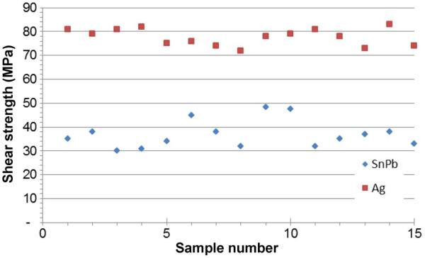
Baseline data on shear strength for 15 63Sn37Pb solder balls were obtained using the testing method described in Fig. 7. 63Sn37Pb solder was dispensed on the 100 μm × 100 μm Au pads (0.5 μm thick) and reflowed by using a standard process as shown in Fig. 5. The shear strength results for 15 SnPb solder bumps are shown in Fig. 19. The average shear strength tested at room temperature was 37 MPa, which is comparable to the 63Sn37Pb industrial standard of 39–41 MPa [41], [42] for IC measured by using lap-shear test (slow speed). After testing 15 Ag bumps, the shear strength as shown in Fig. 19 was found to be 78 MPa on average, which is significantly higher than that of the 63Sn37Pb.
Fig. 19.
Shear strength measurements on 15 bumps each of 63Sn37Pb and Ag.
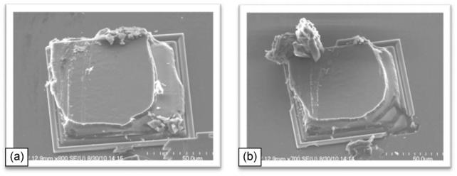
Typical SEM images showing the condition of two bumps after the shear test are shown in Fig. 20. The images indicate failure close to the base of the Ag bumps. The interface between Ag to polysilicon bond pad remained intact, which indicates that the interface strength between Ag and polysilicon was 78 MPa and exceeds the required mechanical reliability of Ag bump. Previous studies have documented that Al is one of the most difficult metals to adhere to for conventional interconnect materials such as solder paste, Au wire, and Au bumps, while Al is a standard CMOS metallization. Several adhesion materials (such as Ti and Cr) are usually needed to adhere well with Al. The DAT by using Ag epoxy adheres well with Al in this study. Therefore, it eliminates the need to have additional adhesion materials.
Fig. 20.
(a) and (b). SEM of two typical Ag bump interconnects after the shear stress characterization.
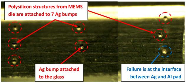
The second shear stress characterization involving both shear and bending stresses—with the schematic setup on Fig. 8—showed that seven bumps failed at the interface between polysilicon pad and silicon as shown in Fig. 21. Polysilicon structures from MEMS die were attached to these seven bumps. Only one bump failed on Ag epoxy bump at the location close to polysilicon pad similar to Fig. 20. The failure of the seven bumps on the polysilicon pads indicated that: 1) the Ag bumps had sufficient strength to endure the amount of applied shear and bending stresses; we did not measure the amount of these combined stresses, but each bump experienced stresses that were significantly larger than 78 MPa: 2) the adhesion between Ag bump and the glass was strong and able to withstand shear stresses larger than 78 MPa.
Fig. 21.
Glass with eight Ag epoxy bump interconnects after shear stress test. Prior to the shear test, it was flip chipped on silicon chips with aluminum bond pads. The seven bumps shown in broken circles showed failure at the polysilicon pad–silicon die interface.
2) Solder Bump Interconnects
It was found that the solder bumps were able to withstand air-jet pressures of 100 psi, which was the limit of the pressure gauge in our air controller. This translated to approximately 689 kPa of shear stress on each bump.
C. Electrical Test
1) Ag Bump Interconnects
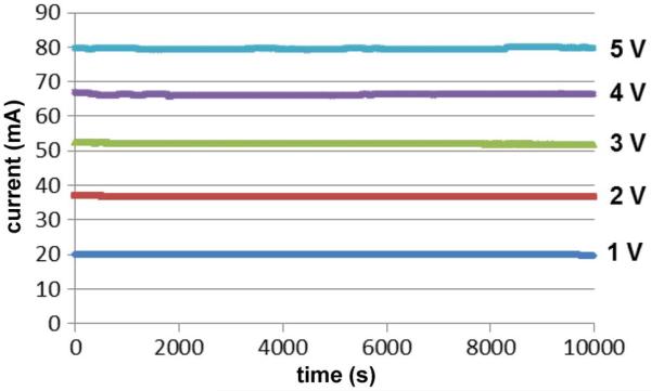
As shown in Fig. 22, for each of the five different voltages applied, the current was constant. For instance, current was 19.96 mA (= 199 A/cm2) at 1 V and 79.4 mA (= 794 A/cm2) at 5 V. This electrical test suggested that the Ag epoxy bumps provide a good and reliable electrical connectivity under room temperature.
Fig. 22.
Measured current over time at different voltages for Ag bumps after flip chip.
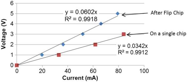
The electrical test showed that the resistance between pad A and D, which completed the whole flip-chip circuit, was 60.2 Ohms as shown by the gradient of the linear approximation in Fig. 23. The resistance between point A and B was also measured by applying voltage and measuring the current. The resistance was found to be 34.2 Ohms. After taking into account the contact resistance between probe tip and the pad, and the line resistance, the resistance of the bump was found to be negligible.
Fig. 23.
Applied voltage versus measured current for electrical test on the Ag interconnect bumps (a) after flip chip and (b) on a single chip.
2) Solder Bump Interconnects
A two-point measurement of the bumps was performed to test the electrical conductivity of the solder bump interconnects after the flip-chip process. The electrical test was performed using a needle probe manipulator and a multimeter. The 4 × 4 array of bumps as shown in Fig. 15 were flip chipped to a 4 × 4 array of pads and then checked for electrical connectivity. It was found that all 16 bumps made electrical contacts via flip-chip joints with negligible resistance at each bump joint. The next possible future improvement is to check the electrical resistance by using four-point wire configuration and applying different environmental stress conditions.
IV. DISCUSSION
In this report, three different novel technologies: 1) Dip and attach technology (DAT) for Ag epoxy; 2) Dispense technology for solder paste (DT); and 3) DPAT for solder paste to develop bump interconnects that meet the needs of flip chip on MEMS have been described. DAT technology process as described in Fig. 2 can also be used for other metal-based epoxy, such as copper or gold, while this report is only focused on the process and characterizations for silver epoxy. The DT and DPAT technologies as described in Figs. 3 and 4 can also be used for other types of solder materials, such as Pb-free solder and SAC305.
Ag epoxy is relatively easy to use due to its fast curing process at 120 °C for 60 s. This technique may be ideal for applications that need a simple and fast process to make interconnects. Solder paste requires an additional reflow process. In this report, we have developed an optimal reflow process that does not produce visible flux contamination and therefore suitable for MEMS application. The optimal reflow process however requires significantly longer time (approximately 1 h) compared with the standard IC reflow process recommended by the manufacturer (Indium Inc.) that only needs 3–5 min. The drawback of long reflow time becomes insignificant in a batch fabrication process. From a cost perspective, solder paste is preferable over Ag epoxy. However, solder paste does not adhere well to all metals. It only adheres well with Au, Cu, and Cr. Ag epoxy, on the other hand is more versatile and adheres well with many surfaces including bare glass and plastic, which is very advantageous for MEMS or BioMEMS application where the pad surface can be made of different type of materials unique for its application.
As demonstrated in Fig. 10, the height of the Ag bump can be increased to any desired level by repeating the DAT steps. This feature is unique and versatile. One of the most problematic issues to package both MEMS and IC in flip-chip MCP (multiple chips on package) configuration is the difference in the overall height of the two different chips after the flip-chip process is completed. Because these two chips come from different vendors that fabricate their devices with different processes, the overall chip height between these two chips can be significantly different. Ideally, these two chips must be flat or have similar collapsed height (gap between the die and substrate, after the assembly is completed) so that the heat sink can be optimally attached to both dies with minimum thermal contact resistance. Furthermore, a significant height difference can crack the dies. By using the Ag bump interconnect technology described in this paper, one can adjust the bump height of the MEMS chip to obtain an acceptable chip height after flip chip. To apply this technology, one must note that the bump height of Ag bump interconnect at each dispensing step is highly dependent on 1) the pad size—the larger the pad size, the taller the bumps, 2) the surface adherence of the pad—the more adhesive the surface, the taller the bumps, and 3) mixture between the Ag particulate and the epoxy—more epoxy generally provides a shorter bump height.
Given the need for HDIs, it is desirable to have a smaller pad size but still maintain a minimum collapsed height of 50 μm. In our experiment, we have demonstrated the ability to create an Ag epoxy bump on 50 μm × 50 μm pad with a bump height as tall as 100 μm after six dispensing steps, i.e., an aspect ratio of 2. We are currently pushing the aspect ratios higher by developing bumps on 25 μm × 25 μm pads with heights of 50 μm or more.
As shown in Figs. 14 and 15, DPAT can produce higher aspect ratio solder bumps compared to DT. Higher aspect ratio is often desirable for MEMS because most MEMS devices have suspended active mechanisms with the height starting from several μm to several hundred μm. In this regard, DPAT process is more applicable for a large movement (out-of-plane) MEMS structure. As shown in Figs. 14 and 15, there is a very thin residue up to 50 μm surrounding the base of the bumps. Because the Cr base pad is very thin (approximately 0.1 μm), a small amount of flux may leak over the pad boundary forming a thin residue. In practice, this residue can be considered as mild and can be regarded as the “keep out zone” distance in the design of MEMS active mechanism. Even this residue can be readily eliminated by having a taller pad such as 1 μm or more as shown in Fig. 16.
The bump strength of the Ag interconnect bumps is 78 MPa significantly higher than the IC standard for solder paste that is 39–41 MPa [41], [42]. The strength of Ag interconnect bumps is expected to be independent of bump geometry. The strength of the solder bumps developed in this paper by DT and DPAT is measured by using an air jet pressure of 689 kPa brought close to the bump without any failure. There is some uncertainty in measurements using the air jet because there is still a small gap (less than 20 μm) between the bump surface and the nozzle tip. It is therefore possible that the strength of the bump is lower than 689 kPa.
Electrical test on the Ag interconnects has shown a fairly constant current over 3 h as shown in Fig. 18. There is a marginal decrease in current of less than 1.5% for over the 3 h of tests. This decrease in current is possibly caused by 1) increase in trace resistance over time due to increase in its temperature, 2) increase in the contact resistance as oxide layer may grow over time on the tip of the probe (made of Tungsten), and 3) capacitive charge occurs between the probe tip and the Au pads which lead to an increase in the resistance value. The test shows that by re-attaching the contact probe to a different contact point within the pad restores the current value back to its original. This confirms that the contact resistance may be directly responsible for the decrease in current over time. The two-point wire test on the Ag interconnect has shown that its resistance is negligible (almost zero). This result is expected because Ag is highly conductive with the conductivity value higher than Au or Cu. The electrical test on the SnPb solder paste has shown negligible change in resistance. We will again validate these results in future studies.
V. CONCLUSION
This report demonstrates three novel techniques to create the FLI structures that can be used as the building platform for MEMS flip-chip packaging: 1) DAT for Ag epoxy interconnect; 2) DT for solder paste interconnect; 3) DPAT for solder paste interconnect. In addition, an optimal reflow process for the solder paste is reported in this paper. This optimal reflow process mitigates the issue of flux contamination that will occur if a standard IC reflow process is used. Compared with prior approaches, the technologies reported in this paper offer distinct advantages such as: 1) the bump creation processes do not require additional postmicrofabrication steps (such as lithography); 2) the technologies can be applied to microfabricated MEMS structures of sizes ranging from tens of μm to hundreds of μm; 3) the processes produce no visible contamination on the MEMS die; 4) the created bumps have aspect ratio of more than one; 5) allows the bond pads to be placed within 25–50 μm of active MEMS structures; 6) gives flexibility in creating bumps of different heights that are predictable and consistent; 7) Ag epoxy process reported here allows adhesion to a wider variety of surfaces such as glass and plastic; and 8) ability of the bumps to withstand shear stresses that are adequate for IC and MEMS chips. The interconnect technologies were tested on a MEMS moveable microelectrodes that have electrical pads of 100 μm × 100 μm. The electrical test demonstrates that the electrical resistance of Ag and solder paste interconnects is negligible.
ACKNOWLEDGMENT
The authors would like to thank M. Baker and M. Okandan for fabricating the MEMS test structures at Sandia National Laboratories, Albuquerque, NM. The authors would also like to thank the Center for Solid State Electronic Research (CSSER) at Arizona State University, Tempe, for the use of their micro-fabrication and SEM facilities. This work was supported by National Institutes of Health Research Grant NS055312-S1.
Biographies

Jemmy Sutanto received the Bachelor’s and Master’s degrees in mechanical engineering from Royal Melbourne Institute of Technology Univer- sity, Melbourne, Australia, and the Ph.D. degree in mechanical engineering from Georgia Institute of Technology, Atlanta.
He was a Senior Packaging Engineer at Intel Corporation with expertise in the high-density first-level interconnects for high-end CPUs. He is currently an Associate Research Scientist in the School of Biomedical and Health Systems Engineering at Arizona State University, Tempe. He is the author or coauthor of 19 journal papers and one book chapter. He holds one U.S. patent, two trade secrets, and five patents pending. His research experiences are in the areas of implantable MEMS, BioMEMS, and microelectronics/MEMS packaging
Dr. Sutanto is a member of the American Society of Mechanical Engineers (ASME) and the Biomedical Engineering Society.

Sindhu Anand received the B.E. (Hons) degree in electrical engineering and the M.Sc. (Hons) degree in biological sciences from the Birla Institute of Technology and Science, Pilani, India, in 2008, and the M.S. degree in biomedical engineering from Arizona State University, Tempe, in 2011, where she is currently working toward the Ph.D. degree in biomedical engineering specializing in the neuro-engineering track.
Her research interests include design of neural interfaces, implantable technologies, and BioMEMS.

Chetan Patel was born in Hyderabad, India, in 1983. He received the B.Sc. degree in bioengineering from Arizona State University, Tempe, in 2007, where he is currently working toward the Ph.D. degree in bioengineering.
His research areas include neural engineering, design and fabrication of MEMS-based neural interfaces, and genetic intervention techniques.

Jit Muthuswamy (M’00–SM’11) received the Master’s degree in electrical engineering, the Master’s degree in biomedical engineering, and the Ph.D. degree in biomedical engineering, all from Rensselaer Polytechnic Institute, Troy, NY.
He is currently an Associate Professor of Bio-engineering in the School of Biological and Health Systems Engineering and an Affiliate Faculty in Electrical Engineering at Arizona State University, Tempe. His research program in developing novel neural interfaces has been supported by NIH, Whitaker Foundation, DARPA, and the Arizona Biomedical Research Commission. His research interests are in neural engineering, neural interfaces, and BioMEMS.
Dr. Muthuswamy is a member of the Society for Neuroscience. He won the Excellence in Neural Engineering Award at the Joint International Conference of the IEEE Engineering and Medicine Society and Biomedical Engineering Society in 2002 and the Outstanding Paer Award (along with coauthor and student, Nathan Jackson) at the the 41st Annual International Microelectronics and Packaging Society Symposium in 2008.
REFERENCES
- 1.Witvrouw A. CMOS-MEMS integration: Why, how and what?; Proc. ICCAD IEEE/ACM; San Jose, CA. 2006. pp. 826–827. [Google Scholar]
- 2.Chen LT, Cheng WH. A novel plastic package for pressure sensors fabricated using the lithographic dam-ring approach. Sens. Actuators A, Phys. 2009 Jan.149:165–171. [Google Scholar]
- 3.Pai RS, Walsh KM. The viability of anisotropic conductive film as a flip chip interconnect technology for MEMS devices. J. Micromech. Microeng. 2005 Jun.15(6):1131–1139. [Google Scholar]
- 4.Candler RN, Park WT, Li HM, Partridge G. Yama, A., Lutz M, Kenny TW. Single wafer encapsulation of MEMS devices. IEEE Trans. Adv. Packag. 2003 Aug.26(3):227–232. [Google Scholar]
- 5.Ayanoor-Vitikkate V, Chen KL, Park WT, Kenny TW. Development of wafer scale encapsulation process for large displacement piezoresistive MEMS devices. Sens. Actuators A, Phys. 2009 Dec.156(2):275–283. [Google Scholar]
- 6.Graham AB, Messana MW, Hartwell PG, Provine J, Yoneoka S, Melamud R, Kim B, Howe RT, Kenny TW. A method for wafer-scale encapsulation of large lateral deflection MEMS devices. J. Microelectromech. Syst. 2010 Feb.19(1):28–37. [Google Scholar]
- 7.Jackson N, Anand S, Okandan M, Muthuswamy J. Nonhermetic encapsulation materials for MEMS-based movable microelectrodes for long-term implantation in the brain. J. Microelectromech. Syst. 2009 Jan.18(6):1234–1245. doi: 10.1109/jmems.2009.2030075. [DOI] [PMC free article] [PubMed] [Google Scholar]
- 8.O’Mahony C, Hill M, Olszewski Z, Blake A. Wafer-level thin-film encapsulation for MEMS. Microelectron. Eng. 2009 Apr-Jun;86(4-6):1311–1313. [Google Scholar]
- 9.Leroy C, Pisani MB, Fritschi R, Hibert C, Lonescu AM. High quality factor copper inductors on wafer-level quartz package for RF MEMS applications; Proc. ESSDERC; Montreux, Switzerland. 2006. pp. 190–193. [Google Scholar]
- 10.Ding H, Yang Z, Chen Z, Zhang R, Yan G. A wafer-level protective technique using glass caps for MEMS gyroscopes; Proc. 8th ICSIC; Shanghai, China. 2006. pp. 2129–2131. [Google Scholar]
- 11.Joseph AJ, Gills JD, Doherty M, Lindgren PJ, Previti-Kelly RA, Malladi RM, Wang PC, Erturk M, Ding H, Gebreselasie EG, McPartlin MJ, Dunn J. Through-silicon vias enable next-generation SiGe power amplifiers for wireless communications. IBM J. Res. Dev. 2008 Nov.52(6):635–648. [Google Scholar]
- 12.Boustedt K, Persson K, Stranneby D. Flip chip as an enabler for MEMS packaging; Proc. 52nd Electron. Compon. Technol. Conf..2002. pp. 124–128. [Google Scholar]
- 13.Basavanhally N, Lopez D, Aksyuk V, Ramsey D, Bower E, Cirelli R, Ferry E, Frahm R, Gates J, Klemens F, Lai W, Low Y, Mansfield W, Pai CS, Papazian R, Pardo F, Sorsch T, Watson P. High-density solder bump interconnect for MEMS hybrid integration. IEEE Trans. Adv Packag. 2007 Nov.30(4):622–628. [Google Scholar]
- 14.Yang HS, Bakir MS. 3D integration of CMOS and MEMS using mechanically flexible interconnects (MFI) and through silicon vias (TSV); Proc. 60th ECTC; Las Vegas, NV. 2010. pp. 822–828. [Google Scholar]
- 15.Zama S, Baldwin DF, Hikami T, Murata H. Flip chip interconnect systems using copper wire stud bump and lead free solder. IEEE Trans. Electron. Packag. Manuf. 2001 Oct.24(4):261–268. [Google Scholar]
- 16.Corbin JS. Finite-element analysis for Solder Ball Connect (SBC) Structural Design Optimization. IBM J. Res. Develop. 1993 Sep.37(5):585–596. [Google Scholar]
- 17.Garrou P. Wafer level chip scale packaging (WL-CSP): An overview. IEEE Trans. Adv. Packag. 2000 May;23(2):198–205. [Google Scholar]
- 18.Vaynman S, Fine ME, Jeannotte DA. Isothermal fatigue of low Tin Lead based solder. Metall. Mater. Trans. A. 1988 Apr.19(4):1051–1059. [Google Scholar]
- 19.Zeng K, Tu KN. Six cases of reliability study of Pb-free solder joints in electronic packaging technology. Mater. Sci. Eng. Rep. 2002 Jun.38(2):55–105. [Google Scholar]
- 20.Indium Inc. Solder Spheres; Dec. 2010. [Online]. Available: http : / / www . indium . com / products / semiconductorpackagingassembly /solderspheres.php. [Google Scholar]
- 21.Zhang F, Li M, Chen WT, Chian KS. An investigation into the effects of flux residues on properties of underfill materials for flip chip packages. IEEE Trans. Compon. Packag. Technol. 2003 Mar.26(1):233–238. [Google Scholar]
- 22.Reichl H, Grosser V. Overview and development trends in the field of MEMS packaging; Proc. 14th IEEE Int. Conf. MEMS; Interlaken, Switzerland. 2001. pp. 1–5. [Google Scholar]
- 23.Goldberg H. How to understand MEMS. R&D Mag. 2002 Jun.44:37–37. [Google Scholar]
- 24.Chen LT. Packaging effect investigation of WL-CSP with a central opening: A case study on pressure sensors. Sens. Actuators A, Phys. 2010 Jan.157(1):47–53. [Google Scholar]
- 25.Maboudian R, Ashurst WR, Carraro C. Self-assembled mono-layers as anti-stiction coatings for MEMS: Characteristics and recent developments. Sens. Actuators A, Phys. 2000 May 15;82(1-3):219–223. [Google Scholar]
- 26.van Spengen WM, Puers R, De Wolf I. A physical model to predict stiction in MEMS. J. Micromech. Microeng. 2002 Sep.12(5):702–713. [Google Scholar]
- 27.Cabruja E, Collado A, Plaza JA, Esteve J. Piezoresistive accelerometers for MCM-Package—Part II: The packaging. J. Micro-electromech. Syst. 2005 Aug.14(4):806–811. [Google Scholar]
- 28.Campabadal F, Carreras JL, Cabruja E. Flip-chip packaging of piezoresistive pressure sensors. Sens. Actuators A, Phys. 2006 Nov.132(1):415–419. [Google Scholar]
- 29.Stark BH, Najafi K. A mold and transfer technique for lead-free fluxless soldering and application to MEMS packaging. J. Microelectro-mech. Syst. 2006 Aug.15(4):849–858. [Google Scholar]
- 30.Plaza JA, Collado A, Cabruja E, Esteve J. Piezoresistive accelerometers for MCM package. J. Microelectromech. Syst. 2002 Dec.11(6):794–801. [Google Scholar]
- 31.Miller DC, Zhang W, Bright VM. Microrelay packaging technology using flip-chip assembly; Proc. 13th Annu. Int. Conf. MEMS.2000. pp. 265–270. [Google Scholar]
- 32.Lin W, Lee YC. Study of fluxless soldering using formic acid vapor. IEEE Trans. Adv. Packag. 1999 Nov.22(4):592–601. [Google Scholar]
- 33.Heschel M, Kuhmann JF, Bouwstra S, Amskov I. Stacking technology for a space constrained microsystem; Proc. 11th Annu. Int. Workshop MEMS.1998. pp. 312–317. [Google Scholar]
- 34.Singh A, Horsley DA, Cohn MB, Pisano AP, Howe RT. Batch transfer of microstructures using flip-chip solder bump bonding; Proc. Int. Conf. TRANSDUCERS; Chicago, IL. 1997. pp. 265–268. [Google Scholar]
- 35.Tilmans HAC, Fullin E, Ziad H, Van de Peer MDJ, Kesters J, Van Geffen E, Bergqvist J, Pantus M, Beyne E, Baert K, Naso F. A fully-packaged electromagnetic microrelay; Proc. 12th IEEE Int. Conf. MEMS; Orlando, FL. 1999. pp. 25–30. [Google Scholar]
- 36.Tomura Y, Bessho Y, Shiraishi T, Itagaki M. Advanced flip chip bonding technique for MCM-L; Proc. 1st Pan Pacific Microelectron. Symp..1996. pp. 125–131. [Google Scholar]
- 37.Hettak K, Morin GA, Stubbs MG. DC-to-50 GHz compensation structure for flip-chip assembled SPST MEMS switch; Proc. IEEE MTT-S Int. MTT; Boston, MA. 2009. pp. 597–600. [Google Scholar]
- 38.Oh KW, Ahn CH. A new flip-chip bonding technique using micromachined conductive polymer bumps. IEEE Trans. Adv. Packag. 1999 Nov.22(4):586–591. [Google Scholar]
- 39.Oh KW, Ahn CH, Roenker KP. Flip-chip packaging using micromachined conductive polymer bumps and alignment pedestals for MOEMS. IEEE J. Sel. Topics Quantum Electron. 1999 Jan-Feb;5(1):119–126. [Google Scholar]
- 40.Li CY, Sauser FE, Azizkhan RG, Ahn CH, Papautsky I. Polymer flip-chip bonding of pressure sensors on a flexible Kapton film for neonatal catheters. J. Micromech. Microeng. 2005 Sep.15:1729–1735. [Google Scholar]
- 41.Jeon SJ, Hyun S, Lee HJ, Kim JW, Ha SS, Yoon JW, Jung SB, Lee HJ. Mechanical reliability evaluation of Sn-37Pb solder joint using high speed lap-shear test. Microelectron. Eng. 2008 Oct.85(10):1967–1970. [Google Scholar]
- 42.Ridout S, Bailey C. Review of methods to predict solder joint reliability under thermo-mechanical cycling. Fatigue Fracture Eng. Mater. Struct. 2007 May;30(5):400–412. [Google Scholar]
- 43.Irwin R, Zhang W, Harsh K, Lee YC. Quick prototyping of flip chip assembly with MEMS; Proc. IEEE RAWCON; Colorado Springs, CO. 1998. pp. 293–296. [Google Scholar]
- 44.Tuantranont A, Liew LA, Bright VM, Zhang J, Zhang W, Lee YC. Bulk-etched surface micromachined and flip-chip integrated micromirror array for infrared applications; Proc. IEEE/LEOS Int. Conf. Opt. MEMS; Kauai, HI. 2000. pp. 71–72. [Google Scholar]
- 45.Muthuswamy J, Okandan M, Jackson N. Single neuronal recordings using surface micromachined polysilicon microelectrodes. J. Neurosci. Methods. 2005 Mar.142(1):45–54. doi: 10.1016/j.jneumeth.2004.07.017. [DOI] [PubMed] [Google Scholar]
- 46.Jackson N, Sridharan A, Anand S, Baker M, Okandan M, Muthuswamy J. Long-term neural recordings using MEMS based movable microelectrodes in the brain. Frontiers Neuroeng. 2010 Jun.3:1–13. doi: 10.3389/fneng.2010.00010. [DOI] [PMC free article] [PubMed] [Google Scholar]


