

Abstract
The next step in the maturing field of nanotechnology is to develop ways to introduce unusual architectural changes to simple building blocks. For nanowires, on-wire lithography (OWL) has emerged as a powerful way of synthesizing a segmented structure and subsequently introducing architectural changes through post-chemical treatment. In the OWL protocol presented here, multisegmented nanowires are grown and a support layer is deposited on one side of each nanostructure. After selective chemical etching of sacrificial segments, structures with gaps as small as 2 nm and disks as thin as 20 nm can be created. These nanostructures are highly tailorable and can be used in electrical transport, Raman enhancement and energy conversion. Such nanostructures can be functionalized with many types of adsorbates, enabling the use of OWL-generated structures as bioactive probes for diagnostic assays and molecular transport junctions. The process takes 13–36 h depending on the type of adsorbate used to functionalize the nanostructures.
INTRODUCTION
Over the past few decades, nanowires and nanorods (the former typically have a smaller diameter and larger aspect ratio, but the terms are often used interchangeably) have become a major research area because of their unusual properties and potential utility in a variety of technologies1–6. Similar to their zero-dimensional counterparts (e.g., nanoparticles and quantum dots), they can now be synthesized and fabricated by many methods including solution-phase synthetic methods, vapor–liquid–solid growth processes and nanolithographic techniques5–12. These first-generation nanowires/rods have provided important fundamental insight into many important scientific problems. However, the development of wire structures with greater architectural complexity (including multiple segments made of different chemical compositions, branched structures, surface coatings and in-wire doping) has led to materials for novel applications, has helped develop physical models of electron and optical transport and has created new synthetic challenges13–15.
In addition to control over the diameter, length and composition of such structures (factors that dramatically influence their physical properties), introducing positive and negative features (e.g., disks shapes or gaps) along the long-wire axes would produce structures with even greater flexibility1,7,9,14–20. In this regard, development of methods for nanowire fabrication and manipulation that are analogous to many powerful types of two-dimensional nanolithographies (e.g., electron beam lithography3, nanoimprint lithography21 and dip-pen nanolithography12) could dramatically increase the scope and utility of such structures. For example, controlling the substructure of one-dimensional nanomaterials will lead to materials with additional functionalities (e.g., plasmonic signatures), which may prove useful in fields such as biodiagnostics, data encoding and light manipulation22–24. This is especially true from a biodetection standpoint where appropriately functionalized plasmonic and electronic materials have been shown to be powerful sensing10,25, detection26,27 and even therapeutic28 agents.
Recently, our group has developed an approach to synthesize nanowires and subsequently to introduce positive and negative architectural features along the long axis of the wire with a high degree of precision and reproducibility20. This method, termed on-wire lithography (OWL), is based on the selective electrodeposition and etching of multicomponent nanowires and allows one to control feature composition and size from the sub-5 nm to many micrometer length scale (Fig. 1). It also allows one to make structures that would be difficult, if not impossible, to fabricate through any other technique16,19,20,29. In addition, structures produced through OWL are dispersible in a wide range of common solvents, which allows for a host of applications not possible with substrate immobilized nanostructures (e.g., dispersible barcodes that can be solution processed and drop cast onto any substrate or device of choice for covert tracking or tagging).
Figure 1.

On-wire lithography protocol. A silver backing is evaporated onto an alumina template (i). A sacrificial silver layer is electrochemically deposited to ensure a clean connection to the evaporated backing (ii). Multicomponent nanowires are grown by electrochemical deposition (iii). The silver backing and alumina template are dissolved and the rods are dispersed onto a glass slide (iv). PECVD or PVD is used to deposit a backing material on one-half of each nanorod (v). The nanorods are sonicated off the surface (vi). The sacrificial segments are then etched (vii). The rods may be functionalized with small molecules and identified by CRM (viiia). Alternatively, the rods can be functionalized with DNA or other biomolecules (viiib). In the case of nucleic acids, the DNA is subsequently suspended in buffer and stabilized with surfactant in the presence of salt (ix). Target DNA strands are hybridized to these rods and identified by CRM (x) (stars represent chromophores generating signal). CRM, confocal Raman spectroscopy.
OWL has been used to fabricate catalytic nanomechanical systems22,23,30, high-throughput devices for the study of molecular electronics31, structures that facilitate light harvesting and energy transfer24 and novel systems for probing the physical underpinnings of the well-known surface-enhanced Raman spectroscopy (SERS) phenomenon32. The OWL technique has even been used to prepare unusual nanogap structures called ‘nanodisk codes’ and electrical ‘nanotraps’. The nanodisk codes consist of pairs of disks oriented along the long wire axis with gaps between the disks forming hotspots for Raman spectroscopy enhancement22. These structures, when functionalized with the appropriate dyes, can be utilized in a novel encoding system where information is stored on the basis of the number and position of the disk codes and the types of dyes they have on their surfaces22. They have been used as dispersible taggants and biological labels for high-sensitivity Raman-based molecular diagnostic assays. The electrical nanotrap consists of a nanowire with a nanometer-scale gap, which can be used to localize charged materials such as oligonucleotides with an appropriate electric field and simultaneously to enhance the Raman spectroscopic signal of materials that enter the gap23. This type of nanostructure is interesting for addressing and probing small quantities of materials that flow near the gap and has been demonstrated in the context of nucleic acids.
A clear protocol to describe how to make such systems, encompassing the OWL process itself and subsequent functionalization and characterization methods, will be an important step toward aiding the development of more advanced systems. Thus, in this protocol, we outline the necessary steps to design, synthesize, functionalize and eventually characterize these systems in a variety of formats including those necessary for SERS studies and biodetection assays. However, the procedures are general and can be readily adapted for a variety of different studies or applications, which should allow OWL to become a powerful tool for many nanotechnology-based investigations.
Applications and limitations
Nanomaterials made by OWL allow for a variety of intriguing applications in nanotechnology. For example, gap-based nanoelectronics, SERS and biosensing modalities have all been realized22,23,29,31, and further applications in these and related fields (e.g., metal-enhanced fluorescence) can be envisioned. This technology will enable the development of more robust, rapid, reliable and sensitive mobile detection schemes for biomolecules. It is also envisioned that the spatially specific ability to enhance spectroscopic information in real time will allow for the study of biological processes. As just one example, we can create a hybrid nanostructure that contains a diode junction and three gold nanodisk pairs. The diode section can be used for electrical measurement of biomolecule binding, and the gold disk pairs can serve as Raman hotspots for spectroscopic measurements. Using this structure, it should be possible to show the parallel electrical and spectroscopic measurement of telomerase binding onto surface-immobilized oligonucleotide receptors and subsequent elongation of the oligonucleotide strands.
The OWL technique has a demonstrated resolution of ~2 nm and is also capable of producing features that are spaced micrometers apart29. In addition (as noted above), a wide variety of metals can be electroplated in the nanowire deposition step. The main challenge of using these metals with OWL is combining several metals into one structure. In this case, care must be taken to choose metals with lattice parameters that are similar enough to ensure adhesion of the two components and to develop etching procedures that are highly selective, even in the presence of multiple metals. In addition, using smaller diameter nanowires (e.g., sub-200 nm pores as a template) may lead to difficulties in redispersing nanostructures during sonication steps after plasma-enhanced chemical vapor deposition (PECVD) or physical vapor deposition (PVD) is performed (Steps 21–23).
Finally, it should be possible to adapt the biodetection strategy on the basis of OWL-generated structures to analytes other than DNA, such as proteins, viruses, metal ions and certain small-molecule analytes. Importantly, in principle, any conventional metal-ligand-binding chemistry can be used to attach chemical or biological species of interest to the OWL structures for the applications listed above.
Experimental design
OWL device fabrication
In the OWL process, anodic aluminum oxide (AAO) membranes (either purchased from commercial vendors, such as Whatman Inc. (part of GE Healthcare) and Synkra Technologies Inc., or fabricated in the lab33) are used as templates to electrochemically deposit nanowires. Cylindrical, aligned, non-intersecting pores permeate the templates and serve as discrete regions for nanowire growth. AAO films can be purchased or prepared with pores ranging in diameter from 500 to 5 nm (Whatman Inc. (part of GE Healthcare) produces templates with ~300 nm pores. Synkera Technologies Inc. produces templates with a variety of pore sizes ranging from 13 to 150 nm) (see refs. 33,34). Although the quality of lab-synthesized templates tends to be better with more uniform pores and narrower pore size distributions (leading to nanowires with more well-defined plasmonic features), for many applications, commercially available AAO templates are often satisfactory1,34. For Whatman (GE Healthcare) templates, better results are achieved if the template is oriented such that Ag is deposited on the side without the polymer support ring. This is because this side has a smoother surface and more uniform pore distribution that makes evaporated Ag films more adherent (see below) and also generates more regular-shaped nanorods.
Deposition of materials into these pores is made possible by first evaporating a metal backing (e.g., Ag, but Cu can also be used) onto one side of the alumina (using high-vacuum thermal or electron-beam evaporation and solid Ag/Cu metal sources) (Fig. 1(i)). This evaporated film acts as a working electrode during nanowire synthesis, and it has been found that an evaporated film thickness ≥150 nm leads to the best electrode contacts in subsequent steps. The templates are then placed in an electrochemical cell (Fig. 2). These cells are commonly custom-built, and the dimensions are given in Figure 2b. These dimensions were chosen to make a cell of manageable size while maximizing the surface area for plating. The electrochemical cells are designed and made in a machine shop using Teflon. The principal aim of the cell is to hold the Ag-coated side of the template in place against the working electrode with the porous side in the electroplating solution along with the reference and counter electrodes. By electrochemically reducing metal ions (most commonly Au+, Ag+, Ni 2+, Pt4+) from the solution into the Ag-backed pores of the template (Fig. 1(ii)), nanowires can be grown with lengths corresponding to the applied charge (Fig. 1(iii)). Typically, cyanide counterion-based solutions work best for noble metal plating, whereas sulfamate and chloride counterion-based solutions are more suitable for Ni and Pt electroplating, respectively. Most vendors (e.g., Technic Inc.) will communicate the metal salts and formulations used in their plating solutions. For the most part, commercial plating solutions designed for electronic applications (as opposed to decorative) work well in this system. In principle, nearly any metal that can be electroplated or formed into a nanrod by electrochemical methods (e.g., Pt, Au, Ag, Cu, Pd, Ru, Rh, Fe, Zn and Ni, to name a few) could be used in the OWL approach. As described in Table 1, one can relate the charge passed to the length of the nanowire grown. Sequential exchanging of plating solutions of different metal ions with one another allows one to deliberately and systematically prepare a large class of segmented nanowires. These segments consist of the actual features to be fabricated and of sacrificial layers that serve as ‘spacer’ segments. In determining the materials that should be used for structural vs. sacrificial layers, care must be taken to determine the chemical reactivity of each metal. For example, Pt and Au are both noble metals and cannot be oxidized easily, whereas Ag and Ni are both readily attacked by acids and oxidants. In general, gaps (generated from the etched sacrificial spacer segments) as small as ~2 nm and positive features (disks, rods) ranging in length from 40 nm to tens of microns can routinely be designed and introduced into the growing nanowire by controlling the electrodeposition rate and time29. Dissolution of the template (usually with a basic solution, see below) and evaporated metal backing (acidic- or peroxide-based solutions, see below) results in the suspension of billions of nanowires in the solution (Fig. 1(iv)). This suspension is then dispersed onto piranha-treated (see below) glass slides (piranha treatment will generate a hydrophilic surface on the glass slide, which will aid in rod dispersion as the solution can wet the surface better), and a backing layer is deposited on the wires by chemical (plasma-enhanced chemical vapor deposition) or physical (physical vapor deposition) deposition methods (Fig. 1(v)). Both conducting (metals) and insulating (oxides) backing materials can be used. With the backing layer in place, wire segments can be redispersed (Fig 1(vi)) and selectively dissolved on the basis of their differences in chemical reactivity (Fig. 1(vii)). This approach results in nanometer scale gaps, disks and disk arrays with precise control over not only the size of the gap but also the thickness, composition and periodicity of the disks. During the procedure, if the investigator wishes, scanning electron microscope (SEM) images of the nanorods can be taken to confirm successful growth, and backing deposition and etching after Steps 13 and 27 (see below), respectively.
Figure 2.

Electrochemical set up. (a) Left to right: Perspective photograph of electrochemical cell, AAO template after Ag evaporation, after first Ag layer, after Au layer and after Ni layer. (b) Dimensions of electrochemical cell. (c) Electrochemical synthesis setup with electrochemical cell on the left, electronics in the center and computer on the right.
TABLE 1.
Parameters for typical nanowire growth.
| Material | Applied potential (versus Ag/AgCl) |
|---|---|
| Au | −920 mV |
| Ag (buffer layer) | −800 mV, 1:10 dilution from stock |
| Ag (rod segment) | −1100 mV, 1:5 dilution from stock |
| Ni | −900 mV |
| Pt | −160 mV |
After synthesis, OWL structures can be routinely functionalized with moieties of interest following a technique modified from the procedure developed in our lab for functionalizing Au nanoparticles (Fig. 1(viii–ix)). These molecules can then be used as reporters in spectroscopic techniques such as Raman spectroscopy (Fig. 1(x))35.
The ratio of nanowire growth length to charge passed is dependent on a variety of factors, the most important being electrode area and pore size. For all figures quoted below, a working electrode surface area of ~1.26 × 10⁻⁴ m2 (calculated by assuming 40% porosity in the AAO template with a 1-cm radius exposed section) with an average pore diameter of 350 nm and a counter electrode consisting of 2 cm2 100 mesh Pt gauze lead to the following relationships (developed from regression lines):
Oligonucleotide probe design
For a three-strand detection scheme, the first DNA strand is bound to the OWL-generated structure and is complementary to one-half of a second target sequence from an organism of interest. The third strand is a ‘reporter’ sequence and is complementary to the other half of the target oligo-DNA strand. This reporter strand is modified with a Raman-active chromophore (many fluorophores and other small molecules are Raman active). In the presence of the target sequence, the three strands (reporter, target and nanostructure-immobilized) hybridize to produce a complete duplex. This three-strand system is useful, because the only way to bring the ‘reporter’ strand in close contact with the Raman-enhancing OWL-generated structure is if the target binds them together (when they are brought in close contact, signal enhancement is ensured, see the ‘Raman characterization’ section below). There is no theoretical limit to the type of nucleic acid that can be bound to the OWL-generated nanostructure surface as long as it is modified with a thiol end group (e.g., PNA, LNA, DNA and RNA can all be envisioned). For all three DNA strands, the oligonucleotide probes should be unique to the target.
Overlaps can be avoided by searching the gene sequence using the NCBI BLAST nucleotide search function (http://blast.ncbi.nlm.nih.gov/Blast.cgi). Each sequence is then carefully checked for potential self-complementarities and hairpin formation, either of which will significantly affect the ability to access and accurately detect the target analyte. For nanoparticle-based detection systems, it is also particularly important to design probe sequences that do not contain terminal G residues, because these bases can form supramolecular complexes that induce nanoparticle aggregation (Note: this process is an aggregation of nanoparticles, not a coalescence; the process is reversible by heating the sample or by modifying the cations that are in solution)36,37. For the nanorod-bound DNA strand, an oligonucleotide ‘spacer’ has been added to the sequence to account for the affinity of the DNA bases to the Au surface because of the presence of amino groups. The spacer element aids in preventing such interactions from interfering with target binding by increasing the likelihood of the recognition sequence portion of the DNA strand from being free from the nanorod surface and being available for binding.
Raman characterization
In Raman spectroscopy, photons interact with molecules and are inelastically scattered. These photons are typically generated by a laser, and the quantities by which photons gain/lose energy are inherent to the molecules they interact with and are also characteristic of the types of chemical bonds present in the molecule. In this manner, Raman spectroscopy can ‘fingerprint’ (and thus detect) chemical moieties with high specificity. However, unenhanced Raman scattering is quite weak (~1 photon in 107 incident photons is Raman scattered). Nanoscale noble-metal substrates (such as, those described in this protocol) are known to enhance the number of Raman-scattered incident photons through a combination of plasmonic–electronic and chemical interactions. Thus, one can take the typically weak Raman scattering process and enhance it with a metal nanostructure to make a very sensitive detection technique (even single molecule). This is why the three-strand detection system is interesting; it brings a very weak Raman-scattering entity into an enhancing field, generating a signal 108 times more intense than the original signal.
However, a powerful laser can still damage analytes. Thus, when imaging specimens with a confocal Raman system, finding the right laser power is critical so that one can observe meaningful signals while limiting sample damage. Typically, laser powers less than ~104 W m−2 are sufficient to observe Raman scattering, especially when using Raman-enhancing substrates such as those described in this protocol. While being high enough to observe the scattering process, this power level will also limit laser-induced sample damage, particularly as long as the laser does not dwell on one point for more than a few seconds. Additional care must be taken when focusing the Raman system, as the optical focal point is sometimes not the optimum z-height for the maximum SERS response. Finally, scan parameters have a dramatic impact on the final image. If a simple ‘on/off’ assay is required, very fast scan parameters (>1 min, integration times of 0.01 to 0.05 s, with 64 lines per image and 64 points per line) can be used, but resolution and signal-to-noise ratios will be affected. A good balance between high throughput (a few minutes per sample) and high quality (signal-to-noise ratios >10:1) can be found in the range of 0.05 to 0.15 s integration times with 128 lines per image and 128 points per line. Using this range as a starting point, one can directly determine the optimum mix of speed and data quality. Finally, it is worth noting that salt, critical to DNA hybridization and functionalization, forms crystals upon sample drying, which can impede imaging. One can avoid this problem by substituting NaCl with ammonium acetate, which is sufficiently volatile to alleviate interfering salt crystallization on the substrate.
MATERIALS
REAGENTS
 CRITICAL Store all reagents as suggested by the vendor.
Reverse osmosis purified >18 MΩ H2O (e.g., NANOpure from Barnstead purified water)
Nuclease-free water, non-DEPC (diethylpryocarbonate)-treated, autoclaved, 0.2 μm filtered (Ambion, Applied Biosystems Inc., cat. no. AM9932)
AAO templates (part of GE Healthcare) (Whatman Inc., 0.2, cat. no. 6809-5022, or 0.02, cat. no. 6809-5002, μm pore diameter, 47-mm outer membrane diameter), or Synkera Technologies Inc. (various sizes, e.g., 150 nm, cat. no. OA-150-50-13) or fabricated in the lab by published methods33,34
Ag and Au wire or a shot (Sigma-Aldrich, cat. no. 204366, 265802) >99.9%).
Cr-coated W filament (Cr >99.9%, Midwest Tungsten Service, cat. no. 3″ Cr-coated rod)
Orotemp 24 RTU (Au, cat. no. 2/0927B), 1025 Ag RTU (Ag, cat. no. x7522000), Nickel sulfamate RTU (Ni, cat. no. 030179) (Technic Inc.)
 CAUTION Au and Ag plating solutions from Technic Inc. contain cyanide, wear personal protective clothing (e.g., nitrile or latex gloves, lab coat, safety glasses) when handling solutions.
(NH3)2PtCl6 (Sigma-Aldrich, cat. no. 204021) (Pt)
Concentrated HNO3 (VWR International, cat. no. 2704-14)
 CAUTION Causes severe burns, wear personal protective clothing (e.g., nitrile or latex gloves, lab coat, safety glasses) when handling solutions.
HCl, concentrated (VWR International, cat. no. HX0603-3)
 CAUTION Can cause burns, wear personal protective clothing (e.g., nitrile or latex gloves, lab coat, safety glasses) when handling solutions.
Methanol, ethanol (>99%) (VWR International, cat. no. BDH1135, BDH1156)
NH4OH, purchased and used as a 28% (vol/vol) solution in H2O (VWR International, cat. no. 3256-05)
 CAUTION Harmful vapors, use in fume hood.
H2O2, purchased and used as 30% (vol/vol) in H2O (VWR International, cat. no. 5240-05)
 CAUTION Causes severe burns, wear personal protective clothing (e.g., nitrile or latex gloves, lab coat, safety glasses) when handling solutions.
NaOH pellets (VWR International, cat. no. BDH0292)
 CAUTION Can cause burns, wear personal protective clothing (e.g., nitrile or latex gloves, lab coat, safety glasses) when handling solutions.
Concentrated H2SO4 (VWR International, cat. no. 2876-45)
 CAUTION Causes severe burns, wear personal protective clothing (e.g., nitrile or latex gloves, lab coat, safety glasses) when handling solutions.
Gases for PECVD: SiH4, 10% in N2 (Scott Specialty Gases, Prod. no. not given, specify to vendor); N2O, 99.9%; N2, 99.9% (Airgas, cat. no. NSCP200, NI UHP6KCT)
 CAUTION SiH4, N2O are toxic, avoid leakage to atmosphere.
Sodium phosphate monobasic (NaH2PO4), molecular biology grade (Sigma-Aldrich, cat. no. S3139)
Sodium phosphate dibasic (Na2HPO4), molecular biology grade (Sigma-Aldrich, cat. no. S3264)
Sodium chloride (NaCl), molecular biology grade (Sigma-Aldrich, cat. no. S3041)
Sodium dodecyl sulfate (SDS), molecular biology grade (Sigma-Aldrich, cat. no. L4390)
Dithiothreitol (DTT), molecular biology grade (Sigma-Aldrich, cat. no. 43815)
Ammonium acetate, molecular biology grade (Prod. no. A1542, Sigma-Aldrich)
Synthetic oligonucleotides (may contain thiol and/or dye moieties) either purchased from Integrated DNA Technologies Inc. or made using Expedite synthesizer with reagents and protocols from Glen Research Inc.
Au nanoparticles, 15 nm (Ted Pella Inc., cat. no. 15704) optional, for procedures requiring oligonucleotide-nanoparticle conjugates
EQUIPMENT
PVD metal evaporator (Edwards Vacuum, cat. no. Edwards Auto 306)
Bioanalytical Systems 100B Signal Generator, cell stand C3, computer control and electrode leads (Bioanalytical Systems, cat. no. E2P-001000, EW-8099)
Pt counter electrode, 99.99+% Pt wire and gauze, 1 mm, gauze, 100 mesh, 99.9% trace metals basis (Sigma-Aldrich, cat. no. 267236)
Ag/AgCl reference electrode RE-5B (Bioanalytical Systems, cat. no. MF-2052)
Aluminum foil (Fisher Scientific Inc., cat. no. 01-213-103)
Teflon cell (made in-house, see Fig. 2)
SEM (Hitachi S4800, Hitachi, cat. no. LEO 1525,)
PECVD apparatus (Plasma Technologies Plasmalab μP also available from Oxford Instruments)
Water bath ultrasonicator model 50 T (VWR International, cat. no. 01T539173)
15 and 50 ml polypropylene vials (BD Falcon, cat. no. 352196, 352070)
1.5 and 2 ml centrifuge tubes (Eppendorf, lo-bind cat. no. 022431021, 022431048).
Heavy glass slide staining dish (Ted Pella, cat. no. 21057)
Autodessicator, dust-free (Secador, cat. no. 31034)
Temperature-controlled Thermomixer R Series (Eppendorf, cat. no. 022670107).
Centrifuge 5424 (Eppendorf, cat. no. 022620401)
NAP-5 column (GE Healthcare, cat. no. 17-0853-01)
UV-vis-NIR spectrophotometer with cuvettes (Thermo Scientific Nanodrop, Varian Cary 100, Varian Cary 5000)
Confocal Raman microscope (CRM) (Witec Instruments Corps, Alpha 300) with laser source (633 nm, HeNe, Coherent Technologies)
REAGENT SETUP
Phosphate adjustment buffer
100 mM phosphate buffer (pH 7.0) consisting of 0.562 g Na2HPO4, 0.125 g NaH2PO4, 50 ml NANOpure H2O. The solution can be stored for up to 3 months at room temperature (20–30 °C) in a sealed glass container.
Surfactant stock solution
0.1% (wt/vol) SDS: 0.01 g SDS, 10 ml NANOpure H2O. The solution can be stored for up to 3 months at room temperature in a sealed glass container.
Salting buffer
2 M NaCl (pH 7.0): 5.844 g NaCl, 50 ml NANOpure H2O. The solution can be stored for up to 3 months at room temperature in a sealed glass container.
Disulfide cleavage buffer
170 mM phosphate buffer (pH 8.0): 1.147 g Na2HPO4, 0.0509 g NaH2PO4 and 50 ml NANOpure H2O. The solution can be stored for up to 3 months at room temperature in a sealed glass container.
Washing buffer 1
10 mM phosphate buffer, 0.01% (wt/vol) SDS (pH 7.0): 0.562 g Na2HPO4, 0.125 g NaH2PO4, 0.05 g SDS and 500 ml NANOpure H2O. The solution can be stored for up to 3 months at room temperature in a sealed glass container.
Assay/washing buffer 2
10 mM phosphate buffer, 300 mM NaCl (pH 7.4): 0.562 g Na2HPO4, 0.125 g NaH2PO4, 8.766 g NaCl and 500 ml NANOpure H2O. The solution can be stored for up to 3 months at room temperature in a sealed glass container.
(NH3)2PtCl6 plating solution
0.1 M in H2O:443.9 mg in 10 ml NANOpure H2O. The solution can be stored for up to 3 weeks at room temperature in a sealed glass container.
4:1:1 Etching solution
4:1:1 mix of methanol, H2O2 (bought as 30% vol/vol), NH3 · H2O (bought as 28% in H2O): 80 ml methanol, 20 ml H2O2 (30% vol/vol), 20 ml NH3 · H2O ratio for 1 template.  CAUTION Etching solution is toxic, corrosive and volatile. Wear personal protective clothing (e.g., nitrile or latex gloves, lab coat, safety glasses) when handling solutions and work in fume hood.
  CRITICAL This solution must be prepared fresh for each template (within 15 min of use).
NaOH solution
3 M in H2O: 60.0 g in 500 ml NANOpure H2O. Solution can be stored for up to 12 months at room temperature in a sealed glass container.
HCl solution
50% (vol/vol) in H2O: 250 ml HCl in 250 ml NANOpure H2O. The solution can be stored for up to 12 months at room temperature in a sealed glass container.
Piranha solution
3:1 mixture of concentrated H2SO4 and H2O2 (30% vol/vol): 150 ml H2SO4, 50 ml H2O2 (30% vol/vol).  CRITICAL This solution must be prepared fresh (within 5 min of use).
  CAUTION Measure out the H2SO4 first and add the H2O2 second. Vigorous reaction occurs upon mixing.
  CAUTION Piranha is extremely reactive and caustic. Will cause burns and vigorously react with organic material! Use only in a fume hood, wear personal protective clothing (e.g., nitrile or latex gloves, lab coat, safety glasses) when handling solutions and keep away from organic chemicals.
Ammonium acetate solution
50 mM solution of ammonium acetate: 38.54 g in 500 ml nuclease-free H2O. The solution can be stored for up to 3 months at room temperature in a sealed glass container.
PROCEDURE
Nanowire synthesis: electrochemical steps  TIMING 1–5 h
-
1∣ Take an AAO template and evaporate a 150 nm-thick Ag backing (a growth rate of ~0.15 nm s−1 will be fast enough to complete deposition in ~30 min, while slow enough to generate high-quality films) on one side.
 PAUSE POINT Templates can be stored after Ag deposition for over 6 months in a container to protect them from dust at room temperature (20–30 °C) (e.g., a petri dish).
 2∣ Place the AAO template with the Ag backing into the electrochemical cell (Fig. 2). Place a thin piece of aluminum foil (~0.1 mm) against the evaporated Ag layer on the AAO template to create a conductive contact to the AAO film. Take care to smooth the aluminum foil (which serves as the working electrode in conjunction with the evaporated Ag layer) with a flat rolling object (e.g., a 15-ml centrifuge tube may be used) before placing the template on top of it.
3∣ Rinse the top of the AAO section with ~2 ml of H2O.
4∣ Assemble the electrodes as shown in Figure 2a (working electrode to the Al foil, counter electrode to the Pt wire, reference electrode to the Ag/AgCl reference).
-
5∣ Dilute the Ag plating solution 1:10 with NANOpure H2O. Add ~8 ml of the Ag plating solution to the electrochemical cell (enough to ensure all electrodes are immersed in the plating solution) and begin the electrodeposition using a potential of −800 mV versus Ag/AgCl reference. Allow ~2.5 °C of charge to pass.
 CAUTION Au and Ag plating solutions from Technic Inc. contain cyanide, wear protective clothing (e.g., nitrile or latex gloves, lab coat, safety glasses) when handling solutions.
 -
6∣ Disconnect the electrodes, discard the plating solution, rinse the electrochemical cell with H2O five times (~8 ml per rinse) and then reconnect the electrodes.
 CRITICAL STEP Ensure that the washing between plating different metals is thorough.
 7∣ Add in the next metal plating solution to the electrochemical cell and begin deposition according to the desired parameters (see Table 1).
-
8∣ Repeat Steps 6 and 7 until the desired structure is created (pictures of how the cell looks after various metal plating steps are shown in Fig. 2).
 PAUSE POINT Rods are stable in the template for months at room temperature.
Nanowire synthesis: etching steps  TIMING 2–6 h
-
9∣ Prepare an etching solution to remove Ag backing. If Ni is present in the structure, a 4:1:1 etching solution can be used. If the structure consists of only noble metals (Au and Pt), HNO3 (concentrated) may be used.
 CAUTION Etching solution is toxic, corrosive and volatile. Wear personal protective clothing (e.g., nitrile or latex gloves, lab coat, safety glasses) when handling solutions, and work in fume hood.
 CRITICAL STEP 4:1:1 etching solution must be made fresh within 15 min of use.
 10∣ Disassemble the cell and place the AAO template (with Ag backing and nanorods inside) in 120 ml (this volume will ensure that enough etchant is present to remove the relevant portions of the entire sample) of the chosen etching solution, taking care to keep the entire template submerged.
11∣ Once the Ag backing is no longer visible, remove the template from the etching solution and rinse with H2O (~20 ml).
-
12∣ Use a razor to cut away excess alumina from the template, and place the template into a 2-ml Eppendorf tube filled with 2 ml of 3 M NaOH. Mix the solution at 24 °C for 6 h with a Thermomixer or sonicate it at 24 °C for 1–2 h until no shards of the template remain.
 CAUTION NaOH can cause burns and wear personal protective clothing (e.g., nitrile or latex gloves, lab coat, safety glasses) when handling solutions.
 -
13∣ Remove the rod solution from the Thermomixer/sonicator, remove the 3 M NaOH by successive rinsing and centrifugation (recommended 1,500g for 30 s) four times with 1 ml of H2O each time. Transfer the rods to a 15-ml BD Falcon centrifuge tube and leave the rods as a suspension in 11 ml of NANOpure H2O. At this point, SEM images can be taken38 of these structures to confirm successful growth. Rods should be discrete and relatively dispersed in the SEM image. Figure 3a is an example of a ‘good’ SEM image of grown nanorods.
 PAUSE POINT Rods are stable in H2O or ethanol for months at room temperature.
 TROUBLESHOOTING
Figure 3.

Field-emission scanning electron microscope images of representative nanorods/nanodisk structures. A representative sample of Au–Ni multisegmented nanorods before deposition of the backing layer and Ni etching (a). Au appears as the lighter contrasting segment. A zoomed in image is on the right. A representative sample of nanorods after the deposition of the backing layer and Ni etching (b). Two zoomed in images of the same rods are on the right, each was taken with different SEM imaging setting: the first shows SiOx-Au contrast, the second shows surface topology.
OWL process  TIMING 12 h
-
14∣ Prepare 160 ml of piranha solution in a glass slide staining dish.
 CAUTION Piranha is extremely reactive and caustic. Will cause burns and vigorously react with organic material! Use only in a fume hood, wear personal protective clothing (e.g., nitrile or latex gloves, lab coat, safety glasses) while handling solutions and keep away from organic chemicals.
 CRITICAL STEP Piranha must be made fresh within 15 min of use.
 15∣ Clean 10 glass slides by immersing them in the piranhafilled glass slide staining dish for 45 min.
16∣ Rinse the glass slides thoroughly with 10 ml of H2O per slide, dry with a stream of N2 for ~10 s and place them on a level surface in a dust-free autodessicator.
17∣ Sonicate the rod solution from Step 13 for 15 s.
-
18∣ Using a pipette, disperse 1 ml of the rod suspension onto each glass slide (1 ml of rod suspension is saved for error-checking/characterization). Let the slides dry in an autodessicator. The side of each slide, which does not contain rods, should be designated as such with a marker (any felt-tip marker, such as a ‘Sharpie’ brand marker).
 PAUSE POINT Rods are stable on the glass slides for months at room temperature.
 19∣ Transfer the glass slides (now with nanorod coatings) to the PECVD chamber.
20∣ Deposit a 40-nm thick SiO2 backing. Typical parameters for SiO2 growth are temperature (300 °C), flow rates of SiH4 and N2O (40 and 400 sccm, respectively) and RF power (12 W). SiO2 growth rate ≈ 15 nm min−1.
21∣ Remove the slides from the PECVD chamber, place one slide in a 50-ml BD Falcon tube filled with 45 ml of either 95% ethanol or absolute ethanol.
22∣ To remove the rods, sonicate the glass slide in ethanol for 90 s. Remove the slide; add another glass slide into a BD Falcon tube.
-
23∣ Repeat Step 22 until all of the slides have been sonicated.
 TROUBLESHOOTING
 24∣ Place the suspension of nanorods in the 50-ml BD Falcon tube in a rack for 8 h at room temperature to allow the nanorods to settle out of solution.
-
25∣ Remove the supernatant until 1 ml of solution is left, transfer to a 2-ml Eppendorf centrifuge tube and wash the rods 2× with 1 ml of 95% ethanol or absolute ethanol (centrifuge for 1 min at 1,500g at room temperature). Resuspend the rods in 2 ml of the necessary etching solution to remove sacrificial layers (typically 2 h for acid etches, e.g., HCl for Ni sections).
 CAUTION Etching solution is toxic, corrosive and volatile. Wear personal protective clothing (e.g., nitrile or latex gloves, lab coat, safety glasses) while handling solutions and work in fume hood.
 CAUTION Take care to leave the top of the rod container vented, as etching conditions can produce gas-phase products.
 TROUBLESHOOTING
 26∣ Ensure the rods are homogeneously suspended in the etching solution during the course of etching, for example, by vortexing and/or by sonicating them.
-
27∣ Rinse/centrifuge (3 min at 1,500g at room temperature) the rods thrice with 1 ml of H2O and then thrice with 1 ml of ethanol. At this point, SEM images can be taken38 of these structures to confirm successful growth. Rods should be discrete and dispersed, and the remaining disk segments should be well supported. Figure 3b is an example of a ‘good’ SEM image of the rods after PECVD and chemical etching.
 PAUSE POINT Rods are stable in solution for months at room temperature.
Functionalization of OWL structure
- 28∣ Functionalization of OWL structures can be carried out using either Option A for small molecules or Option B for nucleic acids.
- Small molecules
 TIMING 3.5 h
- Take a small aliquot (e.g., 200 μl, 20%, ~2 × 10⁸ rods) of a batch of rods and centrifuge/remove the supernatant.
- Make a 1 mM solution of the small molecule of interest in ethanol (e.g., methylene blue, p-mercaptoaniline).
- Resuspend the rods in 1 ml of the solution prepared in Step 28A(ii). Shake in a Thermomixer for 3 h at 800 r.p.m. at 23 °C. Remove × the rods from the Thermomixer and wash them thrice with 1 ml of ethanol.
- Nucleic acids
 TIMING 1 d
- See Box 1 for nucleic acid pre-preparation steps.
- Take a small aliquot (e.g., 200 μl, 20%, ~2 × 10⁸ rods) of a batch of rods and centrifuge/remove the supernatant and resuspend in 1 ml of nuclease-free H2O.
- To the 1 ml aqueous solution of nanorods prepared by OWL (obtained in Step 28B(ii)) (one full template’s yield; ≈1 fM), add freshly synthesized DNA (≈2 OD260). Mix using a Thermomixer for 30 min at 800 r.p.m. at 23 °C.
- To the DNA-nanorod solution, add the phosphate adjustment buffer to bring the final phosphate concentration to 0.01 M in solution.
- To the DNA-nanorod solution, add the SDS solution to bring the SDS concentration to 0.01% (wt/vol) in solution.
- Every 30 min over a 2.5-h time period, add an aliquot of salting buffer so that the final concentration of NaCl in the DNA-nanorod solution is 0.3 M.
-
Allow the DNA-nanorod solution to mix using a Thermomixer in the dark for 2 d at 800 r.p.m. at 23 °C.
 PAUSE POINT The solution is stable for at least 2 weeks at 4 °C when kept in the dark.
 - Wash the DNA-nanorod conjugates to remove excess and unbound DNA strands by centrifuging the nanorod conjugates for 3 min at 5,400g at 24 °C, removing the supernatant and resuspending the pellet in 1 ml of washing buffer 1.
- Repeat Step 28B(viii) twice, and after the third removal of supernatant, resuspend the pellet in 1 ml of assay buffer.
- To this solution, add probe DNA (suspended in assay buffer) and/or target oligonucleotide (B1 OD260 in ~1 ml of assay buffer) and incubate overnight in a Thermomixer at 800 r.p.m. at 23 °C.
- To isolate hybridized DNA-nanorod structures for characterization, centrifuge the mixture at 800g for 3 min at 24 °C, remove the supernatant and resuspend in 1 ml of washing buffer 2. Repeat this process four times, and after the fifth removal of supernatant, resuspend the pellet in a 50-mM solution of ammonium acetate in NANOpure H2O (50–100 μl).
Box 1. PRE-PREPARATION OF DNA FOR SSDNA DETECTION ASSAY.
See the Experimental design section for discussion of the methodology behind the three-strand assay. The procedure in this box may be used for all three DNA oligonucleotide strands used in the assay.
Obtain HPLC-purified, lyophilized oligonucleotides (either from a manufacturer or prepared in house), resuspend the oligonucleotide in 1 ml of fresh, nuclease-free water.
Measure the absorbance of DNA using a UV–visible spectrophotometer and record the absorbance of the 1 ml solution at λmax = 260 nm. This absorbance value corresponds directly to a system of arbitrary units termed optical density (at 260 nm for this system, OD260). For example, if the solution contains 1 OD of DNA, the absorbance value for 1 ml of this solution (using a 10-mm pathlength cuvette) is 1 absorbance unit. (Note: It may be necessary to prepare diluted samples to maintain the analyzed solution absorbance units between 0.01 and 1.0. This absorbance range is crucial to ensure a linear relationship between solution concentration and solution absorbance (i.e., the applicability of Beer’s Law for this system; see below).
Calculate the total amount of DNA in the sample from the optical density units. OD units are easily converted into molarity using a program such as ‘OligoCalc’ (http://www.basic.northwestern.edu/biotools/oligocalc.html), which allows one to accurately determine DNA concentration using the experimentally determined absorbance value and correlating it with the extinction coefficient of the analyzed DNA strand based on sequence length, composition, functional groups and salt concentration parameters.
As DNA is sensitive to degradation both from enzymes free in the environment and from UV light, it is helpful to aliquot the DNA solution into smaller samples, so that only the amount necessary for each experiment is exposed to ambient conditions at any given time. To aliquot the DNA, separate the 1 ml of DNA solution into small Eppendorf tubes (e.g., 250 μl) with 5 OD aliquots in each tube. Lyophilize these solutions, and store them in a light-safe container at −80 °C.
- To prepare DNA for use in the three-strand system, follow Option A for non-thiolated oligonucleotides and Option B for thiolated oligonucleotides.
- Non-thiolated oligonucleotides
- Resuspend the dry, frozen aliquots of DNA in a desired volume of nuclease-free water. The oligonucleotide is now ready for use in the assay
- Thiolated oligonucleotides
-
Prepare 1 ml of 0.1 M of DTT in disulfide cleaving buffer.
 CRITICAL STEP The DTT solution must be prepared fresh once a day. In between use, it may be stored at −20 °C.
 - Resuspend the lyophilized, thiolated-DNA in 20 μl of DTT solution. Protect the solution from light and let stand at for 1–2 h at 24 °C; vortex to mix well.
- 15 min before the completion of disulfide cleavage, begin flushing a NAP-5 column with NANOpure water. At least three column volumes of NANOpure water must flush through before adding DNA.
- Add the 20 μl of DNA solution to the column after all of the water has run through.
- After the 20 μl have flowed into the column, add 500 μl of NANOpure water to the column and continue flowing water into the column.
- Prepare a series of 1.5 ml Eppendorf Lo-Bind centrifuge tubes as collection vials and collect the eluant from the column. The first 5–10 drops of eluant can be discarded, after which collect 4–6 drops of eluant per tube.
- Use a UV–visible spectrophotometer and measure the absorbance at 260 nm to determine the DNA location and concentration using Beer’s Law: A = εbC, where ε is the molar absorptivity, b the cell path length and C the concentration of the solution in units of molarity (ε can be obtained using ‘OligoCalc’ as described above).
-
Calculate the number of moles or ODs of oligonucleotide per tube. The DNA is now ready to be conjugated to the NDC or AuNP surface.
 CRITICAL STEP Freshly cleaved thiols will oxidize in air, and care should be taken to immediately add this purified DNA to the nanomaterial solution for best conjugation.
-
Characterization, SERS  TIMING 10–60 min
29∣ Drop a 40-μl aliquot of a suspension of functionalized OWL structures (from Step 28A(iii) or Step 28B(xi)) onto a piranha-treated glass slide and allow this drop to dry.
-
30∣ Mount the sample on a confocal Raman microscope and focus on individual rods in the sample at ×100 magnification using conventional optics (see Fig. 4).
 TROUBLESHOOTING
 31∣ Set the incident Raman laser power density to ~104 W cm−2 (e.g., by attenuating the laser).
-
32∣ For image scans (x position, y position, intensity), the recommended settings are integration time (0.1 s per pixel), points per line (128) and lines per image (128). Typical collection times are 15 min. For shorter scans (e.g., <4 min), integration times as low as 0.04 s per pixel, with 64 points per line and 64 lines per image can be used.
 TROUBLESHOOTING
Figure 4.
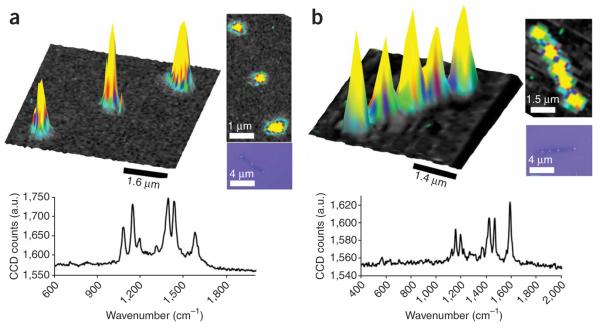
Confocal Raman micrographs of nanodisk SERS-active structures. pMA (p-mercaptoaniline, small molecule) (a) and Cy3-labeled DNA on nanodisk codes (b). Next to each 3D trace is a 2D representation of the same image. Beneath each 3D trace is a Raman micrograph of the spectra taken from the point of median intensity in the sample. a.u., arbitrary units.
 TIMING
Steps 1–8, Nanowire synthesis: electrochemical steps: 1–5 h
Steps 9–13, Nanowire synthesis: etching steps: 2–6 h
Steps 14–27, OWL process: 12 h
Step 28, Functionalization of OWL structure
A, Small molecules timing: 3.5 h
B, Nucleic acids timing: 1 d
Steps 29–32, Characterization, SERS: 10–60 min
 TROUBLESHOOTING
Troubleshooting advice can be found in Table 2.
TABLE 2.
Troubleshooting table.
| Step(s) | Problem | Possible causes | Solution |
|---|---|---|---|
| 13 and 32 | Nanorods are not discrete; they are joined together at one end after initial synthesis |
The junction between the evaporated Ag electrode and the AAO template leaves gaps joining separate pores that must be filled with the Ag buffer layer before nanorods growth. If not enough buffer layer is grown, rods will be joined through these gaps |
Deposit longer Ag buffer layers during the first step of electrosynthesis |
| Rod junctions are poorly formed and not well defined |
If metals ions are present from the pre- vious rod segment, when deposition of the second segment begins, both metal ions will be codeposited |
Rinse the solution more thoroughly between different metal ion solutions for each nanorod component |
|
| 23 | Nanorods will not release from slides during sonication after backing deposition |
The backing layer is binding the nanorods to the substrate surface |
Modify the deposition conditions to deposit a thinner backing layer (backing layers as thin at 20 nm are sufficient but are not as structurally robust as thicker backings) |
| The sonicator is not powerful enough | Try modifying the water level of the sonicator to find resonance; try using a different sonicator |
||
| 25 | Sacrificial layer cannot be etched | The backing layer has enveloped the entire structure; some sections of the structure are catalytically decomposing the etching agent (e.g., Au, Ni catalyze breakdown of H2O2 for Ag etching) |
Deposit a thinner backing layer; use a large excess of etching reagent; switch etching reagent for a fresh solution periodically |
| 30 | Rods are difficult to find by optical imaging |
Salt crystals are inhibiting clear imaging | Use ammonium acetate salts in the final step to reduce salt residue on dried microscopy slides |
ANTICIPATED RESULTS
The OWL process will produce dispersible, discrete, gapped structures. These structures can be suspended in a solution or a cast onto a surface by a variety of methods (e.g., dropping, spin coating). This can be seen in Figure 3, where the initial synthesized nanorods (Fig. 3a) are transformed into disk array structures (Fig. 3b). Note that all of the disks are well supported and present, and each OWL-generated structure is easily dispersible. Upon functionalization and characterization of the rods with confocal Raman spectroscopy, one sees intense Raman activity corresponding to the location of the Raman-active hotspot locations along the disk array (yellow ‘spikes’ against dark flat background, Fig. 4). The intensity of Raman activity depends on a variety of factors, including the geometry of the disk array (including surface roughness), orientation of the disk array relative to laser polarization, laser power and scan rate/integration time, as well as analyte type and packing density. At each peak of Raman intensity, the Raman spectrum itself can be extracted and analyzed. By filtering and/or monitoring specific disk orientations and/or Raman spectral peaks (from different Raman dyes), multiplexing experiments are possible.
ACKNOWLEDGMENTS
C.A.M. acknowledges the National Science Foundation (NSF), the NSSEFF and the AFSOR for support of this research. C.A.M. is also grateful for a NIH Director’s Pioneer Award. M.J.B. acknowledges the 2008 Edward G. Weston ECS Summer Fellowship and NU for a Ryan Fellowship. J.E.M. acknowledges NU for a Presidential Fellowship. K.D.O. acknowledges the NSF for a Graduate Research Fellowship and NU for a Ryan Fellowship.
Footnotes
Reprints and permissions information is available online at http://npg.nature.com/reprintsandpermissions/
References
- 1.Hurst SJ, Payne EK, Qin L, Mirkin CA. Multisegmented one-dimensional nanorods prepared by hard-template synthetic methods. Angew. Chem. Int. Ed. Engl. 2006;45:2672–2692. doi: 10.1002/anie.200504025. [DOI] [PubMed] [Google Scholar]
- 2.Ozin GA, Arsenault AC. Nanochemistry: A Chemical Approach to Nanomaterials. RSC Publishing; Cambridge: 2005. [Google Scholar]
- 3.Gates BD, et al. New approaches to nanofabrication: molding, printing, and other techniques. Chem. Rev. 2005;105:1171–1196. doi: 10.1021/cr030076o. [DOI] [PubMed] [Google Scholar]
- 4.Lieber CM, Wang ZL. Functional nanowires. MRS Bull. 2007;32:99–108. [Google Scholar]
- 5.Xia Y, et al. One-dimensional nanostructures: synthesis, characterization, and applications. Adv. Mat. 2003;15:353–389. [Google Scholar]
- 6.Melosh NA, et al. Ultrahigh-density nanowire lattices and circuits. Science. 2003;300:112–115. doi: 10.1126/science.1081940. [DOI] [PubMed] [Google Scholar]
- 7.Hu J, Ouyang M, Yang P, Lieber CM. Controlled growth and electrical properties of heterojunctions of carbon nanotubes and silicon nanowires. Nature. 1999;399:48–51. [Google Scholar]
- 8.Wu Y, Fan R, Yang P. Block-by-block growth of single-crystalline Si/Si-Ge superlattice nanowires. Nano Lett. 2002;2:83–86. [Google Scholar]
- 9.Gudiksen MS, Lauhon LJ, Wang J, Smith DC, Lieber CM. Growth of nanowire superlattice structures for nanoscale photonics and electronics. Nature. 2002;415:617–620. doi: 10.1038/415617a. [DOI] [PubMed] [Google Scholar]
- 10.Nicewarner-Pena SR, et al. Submicrometer metallic barcodes. Science. 2001;294:137–141. doi: 10.1126/science.294.5540.137. [DOI] [PubMed] [Google Scholar]
- 11.Martin CR. Nanomaterials: a membrane-based synthetic approach. Science. 1994;266:1961–1966. doi: 10.1126/science.266.5193.1961. [DOI] [PubMed] [Google Scholar]
- 12.Piner RD, Zhu J, Xu F, Hong S, Mirkin CA. Dip-pen nanolithography. Science. 1999;283:661–663. doi: 10.1126/science.283.5402.661. [DOI] [PubMed] [Google Scholar]
- 13.Manna L, Scher EC, Alivisatos AP. Synthesis of soluble and processable rod-, arrow-, teardrop-, and tetrapod-shaped CdSe nanocrystals. J. Am. Chem. Soc. 2000;122:12700–12706. [Google Scholar]
- 14.Xiang J, et al. Ge/Si nanowire heterostructures as high-performance field-effect transistors. Nature. 2006;441:489–493. doi: 10.1038/nature04796. [DOI] [PubMed] [Google Scholar]
- 15.Jiang X, et al. InAs/InP radial nanowire heterostructures as high electron mobility devices. Nano Lett. 2007;7:3214–3218. doi: 10.1021/nl072024a. [DOI] [PubMed] [Google Scholar]
- 16.Sioss JA, Keating CD. Batch preparation of linear Au and Ag nanoparticle chains via wet chemistry. Nano Lett. 2005;5:1779–1783. doi: 10.1021/nl051370u. [DOI] [PubMed] [Google Scholar]
- 17.Qian F, Gradecak S, Li Y, Wen C-Y, Lieber CM. Core/multishell nanowire heterostructures as multicolor, high-efficiency light-emitting diodes. Nano Lett. 2005;5:2287–2291. doi: 10.1021/nl051689e. [DOI] [PubMed] [Google Scholar]
- 18.Hu J, Bando Y, Zhan J, Golberg D. Fabrication of silica-shielded Ga-ZnS metal-semiconductor nanowire heterojunctions. Adv. Mat. 2005;17:1964–1969. doi: 10.1002/anie.200462813. [DOI] [PubMed] [Google Scholar]
- 19.Liu S, Tok Jeffrey BH, Bao Z. Nanowire lithography: fabricating controllable electrode gaps using Au–Ag–Au nanowires. Nano Lett. 2005;5:1071–1076. doi: 10.1021/nl050581w. [DOI] [PubMed] [Google Scholar]
- 20.Qin L, Park S, Huang L, Mirkin CA. On-wire lithography. Science. 2005;309:113–115. doi: 10.1126/science.1112666. [DOI] [PubMed] [Google Scholar]
- 21.Chou SY, Krauss PR, Renstrom PJ. Imprint lithography with 25-nanometer resolution. Science. 1996;272:85–87. [Google Scholar]
- 22.Qin L, Banholzer MJ, Millstone JE, Mirkin CA. Nanodisk codes. Nano Lett. 2007;7:3849–3853. doi: 10.1021/nl072606s. [DOI] [PMC free article] [PubMed] [Google Scholar]
- 23.Zheng G, Qin L, Mirkin CA. Spectroscopically enhancing electrical nanotraps. Angew. Chem. Int. Ed. Engl. 2008;47:1938–1941. doi: 10.1002/anie.200705312. [DOI] [PubMed] [Google Scholar]
- 24.Wei W, et al. Surface plasmon-mediated energy transfer in heterograp Au–Ag nanowires. Nano Lett. 2008;8:3446–3449. doi: 10.1021/nl8023164. [DOI] [PMC free article] [PubMed] [Google Scholar]
- 25.Banholzer MJ, Millstone JE, Qin L, Mirkin CA. Rationally designed nanostructures for surface-enhanced Raman spectroscopy. Chem. Soc. Rev. 2008;37:885–897. doi: 10.1039/b710915f. [DOI] [PMC free article] [PubMed] [Google Scholar]
- 26.Patolsky F, Zheng G, Lieber CM. Fabrication of silicon nanowire devices for ultrasensitive, label-free, real-time detection of biological and chemical species. Nat. Protoc. 2006;1:1711–1724. doi: 10.1038/nprot.2006.227. [DOI] [PubMed] [Google Scholar]
- 27.Zheng G, Patolsky F, Cui Y, Wang WU, Lieber CM. Multiplexed electrical detection of cancer markers with nanowire sensor arrays. Nat. Biotechnol. 2005;23:1294–1301. doi: 10.1038/nbt1138. [DOI] [PubMed] [Google Scholar]
- 28.Nie S, Xing Y, Kim GJ, Simons JW. Nanotechnology applications in cancer. Ann. Rev. Biomed. Eng. 2007;9:257–288. doi: 10.1146/annurev.bioeng.9.060906.152025. [DOI] [PubMed] [Google Scholar]
- 29.Qin L, Jang J-W, Huang L, Mirkin CA. Sub-5-nm gaps prepared by on-wire lithography: correlating gap size with electrical transport. Small. 2006;3:86–90. doi: 10.1002/smll.200600386. [DOI] [PubMed] [Google Scholar]
- 30.Qin L, Banholzer MJ, Xu H, Huang L, Mirkin CA. Rational design and synthesis of catalytically driven nanorotors. J. Am. Chem. Soc. 2007;129:14870–14871. doi: 10.1021/ja0772391. [DOI] [PubMed] [Google Scholar]
- 31.Chen X, et al. On-wire lithography-generated molecule-based transport junctions: a new testbed for molecular electronics. J. Am. Chem. Soc. 2008;130:8166–8168. doi: 10.1021/ja800338w. [DOI] [PMC free article] [PubMed] [Google Scholar]
- 32.Qin L, et al. Designing, fabricating, and imaging Raman hot spots. Proc. Natl Acad. Sci. USA. 2006;103:13300–13303. doi: 10.1073/pnas.0605889103. [DOI] [PMC free article] [PubMed] [Google Scholar]
- 33.Masuda H, Fukuda K. Ordered metal nanohole arrays made by a two-step replication of honeycomb structures of anodic alumina. Science. 1995;268:1466–1468. doi: 10.1126/science.268.5216.1466. [DOI] [PubMed] [Google Scholar]
- 34.Payne EK, Shuford KL, Park S, Schatz GC, Mirkin CA. Multipole plasmon resonances in gold nanorods. J. Phys. Chem. B. 2006;110:2150–2154. doi: 10.1021/jp056606x. [DOI] [PMC free article] [PubMed] [Google Scholar]
- 35.Hill HD, Mirkin CA. The bio-barcode assay for the detection of protein and nucleic acid targets using DTT-induced ligand exchange. Nat. Protoc. 2006;1:324–336. doi: 10.1038/nprot.2006.51. [DOI] [PubMed] [Google Scholar]
- 36.Li Z, Mirkin CA. G-quartet-induced nanoparticle assembly. J. Am. Chem. Soc. 2005;127:11568–11569. doi: 10.1021/ja053547s. [DOI] [PubMed] [Google Scholar]
- 37.Mirkin CA, Letsinger RL, Mucic RC, Storhoff JJ. A DNA-based method for rationally assembling nanoparticle into macroscopic materials. Nature. 1996;382:607–609. doi: 10.1038/382607a0. [DOI] [PubMed] [Google Scholar]
- 38.Goldstein J, et al. Scanning Electron Microscopy and X-ray Microanalysis. 3rd ed Springer Science & Business Media, Inc.; New York: 2003. [Google Scholar]