Abstract
A gate-controlled metal-semiconductor barrier modulation and its effect on carrier transport were investigated in two-dimensional (2D) transition metal dichalcogenide (TMDC) field effect transistors (FETs). A strong photoresponse was observed in both unipolar MoS2 and ambipolar WSe2 FETs (i) at the high drain voltage due to a high electric field along the channel for separating photo-excited charge carriers and (ii) at the certain gate voltage due to the optimized barriers for the collection of photo-excited charge carriers at metal contacts. The effective barrier height between Ti/Au and TMDCs was estimated by a low temperature measurement. An ohmic contact behavior and drain-induced barrier lowering (DIBL) were clearly observed in MoS2 FET. In contrast, a Schottky-to-ohmic contact transition was observed in WSe2 FET as the gate voltage increases, due to the change of majority carrier transport from holes to electrons. The gate-dependent barrier modulation effectively controls the carrier transport, demonstrating its great potential in 2D TMDCs for electronic and optoelectronic applications.
Compared to graphene which cannot achieve the low off-state and saturated on-state currents due to its zero bandgap1,2,3, transition metal dichalcogenides (TMDCs) have opened up new opportunities for two-dimensional (2D) electronics and optoelectronics such as transistors4,5, memories6,7, integrated circuits8,9, photodetectors10,11, and electro-luminescent devices12 etc., because of their selectable electronic properties ranging from metallic to semiconducting, and tunable bandgaps with layer-dependence13,14. Particularly for semiconducting TMDCs such as MoX2 and WX2 compounds (X is a chalcogen), their sub-nanometer thickness with sizable bandgaps around 1–2 eV can provide high on/off ratios and more efficient control over switching. The immunity of short-channel effect and ultralow power dissipation which are made possible by using 2D materials can break through the scaling limit for future transistor miniaturization15,16. For example, MoS2 as a representative n-type semiconducting TMDC has an indirect bandgap of 1.3 eV in bulk structure but a direct bandgap of 1.8 eV in single-layer form13. Owing to the thickness-dependent bandgap modulation, the triple-layer MoS2 shows a strong photoresponse for red light detection, while the single- and double-layer MoS2 are preferred for green light detection11. The direct bandgap in single-layer MoS2 also gives rise to photo- and electro-luminescence, posing the potential for novel 2D optoelectronic devices such as light detectors and emitters12. Another example, WSe2 with the bandgap of 1.2 eV in bulk structure and 1.7 eV in single-layer form13 has also been studied for transistor17,18 and photovoltaic applications13. Although carrier mobility of MoS2 and WSe2 are relatively low, it can be improved significantly by the optimized or chemically doped metal contacts17,19, dielectric engineering via high-k materials4,17, and formation of an inversion channel5 etc.
In this work, both few-layer MoS2 and WSe2 flakes were applied to the back-gate field effect transistors (FETs) with Ti/Au metallization, and their carrier transport was investigated over a wide range of drain voltage (0 to 5 V) and gate voltage (−50 to 50 V) to demonstrate its strong dependency on bias modulation. To understand the modulation effects more clearly, we investigated the formation of Schottky and ohmic contacts from the MoS2 and WSe2 FETs, by measuring the energy barriers of the carriers at the contacts and relating them to the carrier transport and photo-response of these FETs.
Results
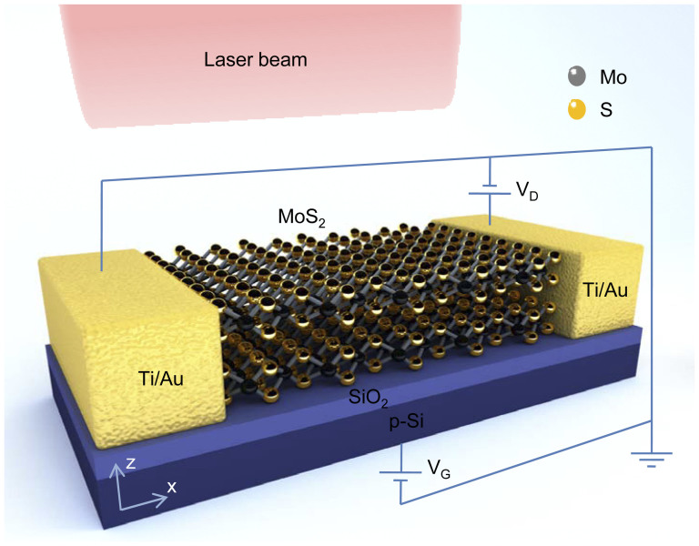
Thin MoS2 and WSe2 flakes are obtained by mechanical exfoliation from the bulk crystals, and transferred to a p-type Si substrate (1.0–10.0 Ωcm) with 90-nm-thick thermally grown SiO2 surfaces. The back-gate FET devices are fabricated via electron beam lithography (EBL) with Ti/Au (5 nm/50 nm) electrodes deposited by electron beam evaporation, as shown in Fig. 1. The MoS2 flake has the thickness of ~3 nm measured by atomic force microscopy (AFM), and its Raman spectrum shows two typical peaks (E2g1 and A1g) with a large separation of 23 cm−1. The WSe2 flake has the thickness of ~9 nm, and only shows a single peak at around 250 cm−1 20 (Supplementary Information Fig. S1). These suggest the few-layer structure of both MoS2 and WSe2 flakes.
Figure 1. TMDC FETs under laser illumination.
Schematic perspective view and circuit diagram of a TMDC FET under laser illumination with few-layer MoS2 as channel layer.
The electrical characterization of MoS2 and WSe2 FETs is performed by a semiconductor parameter analyzer in a vacuum condition (10 mTorr) at the room temperature. The optoelectronic performance is analyzed by combining a dot laser (655 nm, 15 mW) illuminating system, where the photocurrent (PC) signal is defined as the difference of drain current (ID) in dark and laser illuminating environments at certain drain and gate voltages (VD and VG). The ID-VG transfer characteristics of MoS2 FET illustrate an n-type unipolar carrier transport. As a comparison, an asymmetric ambipolar transport with the dominant electron conduction is observed in WSe2 FET. The trapping-induced hysteresis with voltage shift of 2 and 10 V suggests an equivalent trap density of 4.79 × 10¹¹ and 2.40 × 1012 cm−2 in MoS2 and WSe2 FETs, respectively21 (Supplementary Information Fig. S2). Before measuring the PC of TMDC FETs, a calibration is performed by measuring the photoresponse of metal and metal/SiO2 interface. The identical electrical performance in both dark and illuminating environments excludes the photoresponsive contributions of metal and metal/SiO2 interface, and suggests that all the PCs are generated in TMDC FETs.
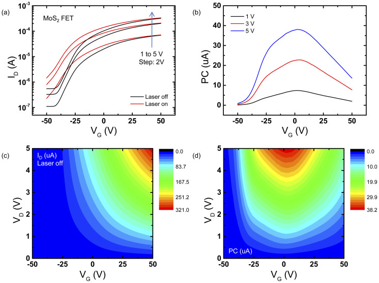
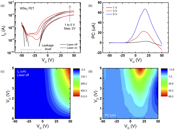
The carrier transport in both MoS2 and WSe2 FETs is investigated over a wide range of VD (0 to 5 V) and VG (−50 to 50 V), as shown in Fig. 2 for MoS2 FET and in Fig. 3 for WSe2 FET. In the dark environment, the carrier transport is maximized at the high VG (50 V) and VD (5 V) levels in both MoS2 and WSe2 FETs due to the high carrier density induced by electrical gating and the high electric field along the channel for carrier drift, respectively. This is consistent with the carrier transport theory in conventional semiconductor FETs. As a comparison, it is interesting to find out that the PC generation in both MoS2 and WSe2 FETs is not proportional to the carrier transport in dark environment. The PC peaks under illumination are located at the high VD (5 V in both MoS2 and WSe2 FETs), owing to the high electric field along the channel for separating the photo-excited charge carriers. However, the PC peaks are located at the different certain VG (~0 V in MoS2 FET and ~20 V in WSe2 FET), not at the VG of the maximized carrier transport (~50 V in both MoS2 and WSe2 FETs). Therefore, the conventional carrier transport theory is not suitable to explain the transport of photo-excited charge carriers, and thus a new mechanism is required to interpret the gate-dependent photoresponse in TMDCs.
Figure 2. Photoresponse of transfer characteristic in MoS2 FET.
(a), (b) Transfer characteristic of MoS2 FET in dark and illuminating environments in forward sweep for various VD levels, and the corresponding PCs. (c), (d) Mapping of dark current (laser off) and PC as functions of VD and VG.
Figure 3. Photoresponse of transfer characteristic in WSe2 FET.
(a), (b) Transfer characteristic of WSe2 FET in dark and illuminating environments in forward sweep for various VD levels, and the corresponding PCs. (c), (d) Mapping of dark current (laser off) and PC as functions of VD and VG.
Discussion
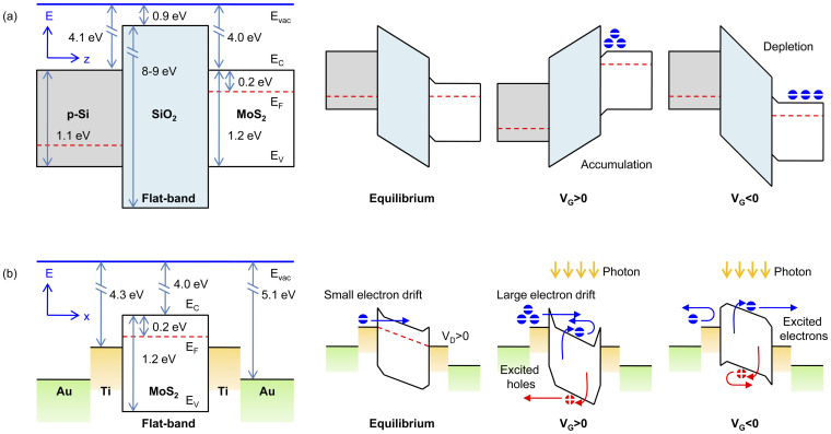
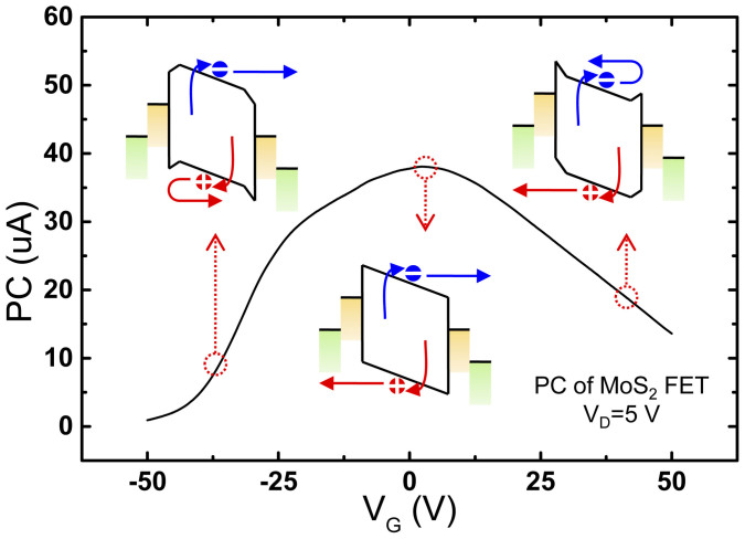
A gate-controlled metal-semiconductor barrier modulation is proposed to interpret the carrier transport of both MoS2 and WSe2 under illumination. Here we take the MoS2 FET as an example due to its unipolar carrier transport which is simpler compared to the case of ambipolar WSe2 FET. Firstly, the energy band diagrams of MoS2 FET illustrate the electrical gating effect along the vertical axis for various VG conditions, as shown in Fig. 4(a). When VG > 0, the electrons are attracted to the interface between MoS2 and SiO2 to form an accumulation layer. When VG < 0, the electrons are repelled from the interface to establish a depletion layer. Further increasing the negative VG may create an inversion channel which gives rise to the high mobilities5. Secondly, the metal-semiconductor barriers at both source and drain ends are modulated capacitively by the gate, as shown in Fig. 4(b). The barriers are induced due to a mismatch between the workfunctions of MoS2 and Ti, and they can be enlarged or reduced by applying the negative or positive VG, respectively. The barrier height (ϕms) at the equilibrium can be theoretically estimated as ΦM–χ22, where ΦM is the work function of Ti (4.3 eV), and χ is the electron affinity of MoS2 (4.0 eV)19. In MoS2 FET, ϕms is estimated as 0.3 eV, which is in agreement with the theoretical estimation22,23 and experimental results obtained by temperature-dependent electrical measurements8,19,24,25 previously. Thirdly, the carrier transports in both dark and illuminating environments are strongly affected by the gate-dependent barrier modulation. For the electron drift along the channel driven by a positive VD, the barriers are reduced with increasing VG, allowing the electrons to transport through by tunneling effect or thermionic emission in the dark environment. As a comparison, for the photon-excited charge carriers generated within the channel under illumination, the barriers only allow the electron collection at the drain end, but suppress the hole collection at the source end when VG < 0, and vice versa when VG > 0. Therefore, the PC generation is still relatively small at the high positive and negative VG levels due to the inefficient carrier collection. However, there should be an optimized VG condition where the barriers for both electron and hole collection are minimized at the source and drain ends concurrently, contributing to a peak PC generation. This gate-controlled barrier modulation can thoroughly interpret the gate-dependent photoresponse of MoS2 FET, as shown in Fig. 5. Similarly, it can also be applied to WSe2 FET due to the analogous energy bandgap. Finally, the channel current under illumination, which is the sum of both dark current and PC, shows the gate dependence following a combined barrier modulation for both electron drift and photo-excited charge carriers.
Figure 4. Energy band diagrams of MoS2 FET.
The energy band diagrams along (a) the vertical axis (z) and (b) the horizontal axis (x) illustrate various gating conditions, including flat-band, equilibrium (VG = 0), accumulation (VG > 0) and depletion (VG < 0). The blue solid line and red dash line denote the vacuum and Fermi levels, respectively. The blue and red arrows indicate the transport of electrons and holes.
Figure 5. Gate-dependent barrier modulation in MoS2 FET.
The barriers at both source and drain ends can be minimized at certain VG, which promote the collection of photo-excited charge carriers and contribute to a PC peak. The PC generation as a function of VG in WSe2 FET can also be interpreted analogously.
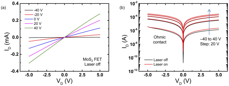
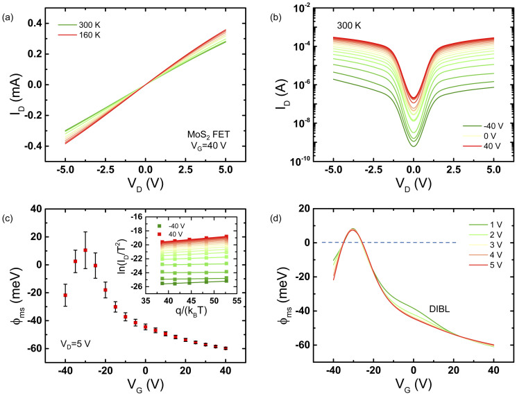
To quantitatively analyze the barrier modulation, the effective value of (ϕms) between metal and TMDC is obtained by testing the temperature dependence of channel current25,26. A typical ohmic contact behavior in the ID-VD output characteristics of MoS2 FET and its photoresponse are observed at various VG levels, as shown in Fig. 6. For the carrier transport through a metal-semiconductor barrier, the tunneling effect dominates when the semiconductor is highly doped, whereas the thermionic emission dominates when the semiconductor is slightly or moderately doped. Since the MoS2 is intrinsic in this work, the current-voltage relation is determined by thermionic emission as26
 |
where A is the area of the contact junction, A* is the effective Richardson constant, q is the electronic charge, kB is the Boltzmann constant, and T is the temperature. Considering the electron transport from the source to the drain ends, a back-to-back metal-semiconductor-metal contact is formed, and the carrier transport is mainly affected by the contact condition at the drain end due to the applied VD. Under a high VD, the contact at the drain end is reversely biased [exp(−qVD/kBT) ≪ 1], and ID becomes proportional to T2exp(−ϕms/kBT). A linear relation between ln(ID/T2) and q/kBT can be plotted for various VG levels, and the gate-dependent ϕms for a given VD is estimated from the slope of each curve, as shown in Fig. 7. ϕms has a very low value on the order of 10 meV, which is in agreement with the presence of ohmic contact. ϕms also shows a reduction as VG increases, being consistent with the barrier modulation theory. Moreover, a reduction of ϕms with increasing VD is clearly observed near zero gate voltage, suggesting a drain-induced barrier lowering (DIBL) effect in MoS2 FET. Besides, it is noted that ϕms is reduced at very high negative VG. This may be induced by the increased minority carrier density during the formation of inversion layer.
Figure 6. Ohmic contact and its photoresponse in MoS2 FET.
(a), (b) Output characteristic of MoS2 FET for various VG levels in linear scale and its photoresponse in logarithmic scale, suggesting an ohmic contact behavior.
Figure 7. Extraction of barrier height in MoS2 FET.
(a), (b) Output characteristic of MoS2 FET for various temperatures (160 to 300 K with a step of 20 K) and VG (−40 to 40 V with a step of 5 V) levels. (c), (d) Effective barrier height as a function of VG for various VD levels. Inset of (c): Temperature-dependent current characteristics and their corresponding linear fit for various VG levels at VD of 5 V.
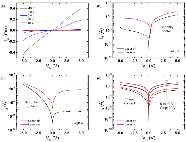
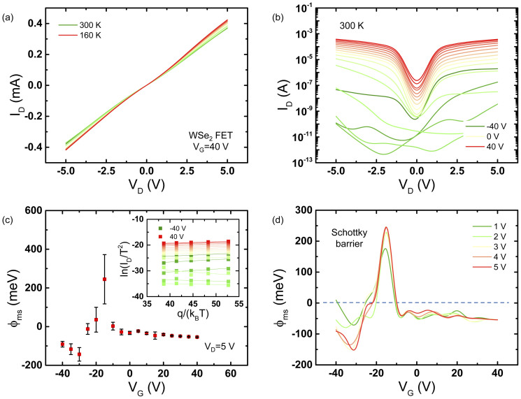
For the WSe2 FET, a transition from Schottky to ohmic contact is observed, as shown in Fig. 8. The current-voltage relation shows the Schottky contact behavior with opposite polarities at VG of −40 and −20 V, but then shows the ohmic contact behavior as VG increases from 0 V to 40 V. Considering the ambipolar transport of WSe2, this Schottky-to-ohmic contact transition may be induced by the change of majority carrier transport from holes at negative VG to electrons at positive VG (see Fig. 3(a)). The experimental value of ϕms is obtained as a function of VG, as shown in Fig. 9. ϕms shows a dip near −40 V and a peak near −20 V, indicating the Schottky contact with opposite polarities. As VG increases further, the value of ϕms is reduced from the order of 100 to 10 meV, suggesting a transition from Schottky to ohmic contact.
Figure 8. A Schottky-to-ohmic contact transition and its photoresponse in WSe2 FET.
(a) Output characteristic of WSe2 FET for various VG levels in linear scale. (b–d) Photoresponse of output characteristic in logarithmic scale indicates a transition from Schottky contact to ohmic contact as VG increases.
Figure 9. Extraction of barrier height in WSe2 FET.
(a), (b) Output characteristic of WSe2 FET for various temperatures (160 to 300 K with a step of 20 K) and VG (−40 to 40 V with a step of 5 V) levels. (c), (d) Effective barrier height as a function of VG for various VD levels. Inset of (c): Temperature-dependent current characteristics and their corresponding linear fit for various VG levels at VD of 5 V.
In conclusion, the bias-controlled barrier modulation in TMDC FETs and its effect on carrier transport were investigated over a wide range of gate and drain voltages. Being disproportionate to the conventional carrier transport in dark environment, a strong photoresponse was observed at the certain gate and drain voltages due to the change in barrier heights between metal and TMDC materials which resulted in ohmic contact or Schottky contact. The gate-dependent barrier modulation effectively controlled the carrier transport in MoS2 and WSe2.
Methods
Fabrication of TMDC FET devices
Both MoS2 and WSe2 thin flakes were mechanically exfoliated from bulk crystals by using scotch tapes. Before the transfer procedure, the silicon wafer was pre-cleaned by sonication in acetone, isopropyl alcohol, and deionized water, followed by drying in nitrogen flow and heating on hot plate to remove the moisture. Electrodes were patterned by standard EBL procedure. 5-nm-thick Ti and 50-nm-thick Au were deposited by electron beam evaporation, followed by a post-annealing in N2 environment at 300°C for 1 hour to improve the metal contact.
Author Contributions
H.M.L. and W.J.Y. conceived the research project, supervised the experiment and wrote the paper. H.M.L., D.Y.L. and M.S.C. performed device fabrication. H.M.L. performed electrical and optoelectronic characterization. D.Q. performed AFM analysis. X.L. performed theoretical simulation. C.H.R. performed Raman spectrum analysis.
Supplementary Material
SI
Acknowledgments
This work is supported by the Basic Science Research Program through the National Research Foundation of Korea (NRF) (2009-0083540, 2011-0010274, 2013-015516), and by the Global Frontier R&D Program (2013-073298) on Center for Hybrid Interface Materials (HIM) funded by the Ministry of Science, ICT & Future Planning.
References
- Schwierz F. Graphene transistors. Nature Nanotech. 5, 487–496 (2010). [DOI] [PubMed] [Google Scholar]
- Bonaccorso F., Sun Z., Hasan T. & Ferrari A. C. Graphene photonics and optoelectronics. Nature Photo. 4, 611–622 (2010). [Google Scholar]
- Castro Neto A. H. & Novoselov K. New directions in science and technology: two-dimensional crystals. Rep. Prog. Phys. 74, 082501 (2011). [Google Scholar]
- Radisavljevic B., Radenovic A., Brivio J., Giacometti V. & Kis A. Single-layer MoS2 transistors. Nature Nanotech. 6, 147–150 (2011). [DOI] [PubMed] [Google Scholar]
- Kim S. et al. High-mobility and low power thin-film transistors based on multilayer MoS2 crystals. Nature Commun. 3, 1011 (2012). [DOI] [PubMed] [Google Scholar]
- Choi M. S. et al. Controlled charge trapping by molybdenum disulphide and graphene in ultrathin heterostructured memory devices. Nature Commun. 4, 1624 (2013). [DOI] [PubMed] [Google Scholar]
- Bertolazzi S., Krasnozhon D. & Kis A. Nonvolatile memory cells based on MoS2/graphene heterostructures. ACS Nano 7, 3246–3252 (2013). [DOI] [PubMed] [Google Scholar]
- Yu W. J. et al. Vertically stacked multi-heterostructures of layered materials for logic transistors and complementary inverters. Nature Mater. 12, 246–252 (2013). [DOI] [PMC free article] [PubMed] [Google Scholar]
- Wang H. et al. Integrated circuits based on bilayer MoS2 transistors. Nano Lett. 12, 4674–4680 (2012). [DOI] [PubMed] [Google Scholar]
- Lopez-Sanchez O., Lembke D., Kayci M., Radenovic A. & Kis A. Ultrasensitive photodetector based on monolayer MoS2. Nature Nanotech. 8, 497–501 (2013). [DOI] [PubMed] [Google Scholar]
- Lee H. S. et al. MoS2 nanosheet phototransistors with thickness-modulated optical energy gap. Nano Lett. 12, 3695–3700 (2012). [DOI] [PubMed] [Google Scholar]
- Sundaram R. S. et al. Electroluminescence in single layer MoS2. Nano Lett. 13, 1416–1421 (2013). [DOI] [PubMed] [Google Scholar]
- Wang Q. H., Kalantar-Zadeh K., Kis A., Coleman J. N. & Strano M. S. Electronics and optoelectronics of two-dimensional transition metal dichalcogenides. Nature Nanotech. 7, 699–712 (2012). [DOI] [PubMed] [Google Scholar]
- Chhowalla M. et al. The chemistry of two-dimensional layered transition metal Dichalcogenide nanosheets. Nature Chem. 5, 263–275 (2013). [DOI] [PubMed] [Google Scholar]
- Liu H., Neal A. T. & Ye P. D. Channel length scaling of MoS2 MOSFETs. ACS Nano 6, 8563–8569 (2012). [DOI] [PubMed] [Google Scholar]
- Liu H., Gu J. & Ye P. D. MoS2 nanoribbon transistors: transition from depletion mode to enhancement mode by channel-width trimming. IEEE Electron Device Lett. 33, 1273–1275 (2012). [Google Scholar]
- Fang H. et al. High-performance single layered WSe2 p-FETs with chemically doped contacts. Nano Lett. 12, 3788–3792 (2012). [DOI] [PubMed] [Google Scholar]
- Liu W. et al. Role of metal contacts in designing high-performance monolayer n-type WSe2 field effect transistors. Nano Lett. 13, 1983–1990 (2013). [DOI] [PubMed] [Google Scholar]
- Das S., Chen H.-Y., Penumatcha A. V. & Appenzeller J. High performance multilayer MoS2 transistors with scandium contacts. Nano Lett. 13, 100–105 (2013). [DOI] [PubMed] [Google Scholar]
- Tonndorf P. et al. Photoluminescence emission and Raman response of monolayer MoS2, MoSe2, and WSe2. Optics Exp. 21, 4908–4916 (2013). [DOI] [PubMed] [Google Scholar]
- Wang H., Wu Y., Cong C., Shang J. & Yu T. Hysteresis of electronic transport in graphene transistors. ACS Nano 4, 7221–7228 (2010). [DOI] [PubMed] [Google Scholar]
- Choi W. et al. High-detectivity multilayer MoS2 phototransistors with spectral response from ultraviolet to infrared. Adv. Mater. 24, 5832–5836 (2012). [DOI] [PubMed] [Google Scholar]
- Lee K. et al. Electrical characteristics of molybdenum disulfide flakes produced by liquid exfoliation. Adv. Mater. 23, 4178–4182 (2011). [DOI] [PubMed] [Google Scholar]
- Chen J.-R. et al. Control of Schottky barriers in single layer MoS2 transistors with ferromagnetic contacts. Nano Lett. 13, 3106–3110 (2013). [DOI] [PubMed] [Google Scholar]
- Yang H. et al. Graphene barristor, a triode device with a gate-controlled Schottky barrier. Science 336, 1140–1143 (2012). [DOI] [PubMed] [Google Scholar]
- Neamen D. A. Semiconductor physics and devices: basic principles. 3rd ed. McGraw-Hill (2003).
Associated Data
This section collects any data citations, data availability statements, or supplementary materials included in this article.
Supplementary Materials
SI


