Abstract
We investigated the bipolar resistive switching characteristics of the resistive random access memory (RRAM) device with amorphous carbon layer. Applying a forming voltage, the amorphous carbon layer was carbonized to form a conjugation double bond conductive filament. We proposed a hydrogen redox model to clarify the resistive switch mechanism of high/low resistance states (HRS/LRS) in carbon RRAM. The electrical conduction mechanism of LRS is attributed to conductive sp2 carbon filament with conjugation double bonds by dehydrogenation, while the electrical conduction of HRS resulted from the formation of insulating sp3-type carbon filament through hydrogenation process.
Keywords: Carbon, Hydrogen redox, Conjugation double bond, RRAM
Background
Recently, portable electronic products which are combined memory circuits [1-3], display design [4,5] and IC circuits have popularized considerably in the last few years. To surmount the technical and physical limitation issues of conventional charge-storage-based memories [6-11], the resistance random access memory (RRAM) is constructed of an insulating layer sandwiched by two electrodes. This structure is a great potential candidate for next-generation nonvolatile memory due to its superior characteristics such as lesser cost, simple structure, high-speed operation, and nondestructive readout [12-21].
The carbon-based resistive memory (C-RRAM) has emerged as one of a few candidates with high density and low power. The resistive switching of C-RRAM relies on the formation and rupture of filaments due to redox chemical reaction mechanism, which is similar to most other reported RRAM devices [22-43].
In this paper, we investigated the resistive switching characteristics of amorphous carbon films prepared by RF magnetron sputter deposition technique for nonvolatile memory applications. Reliable and reproducible switching phenomena of the amorphous carbon RRAM with Pt/a-C:H/TiN structure were observed. In addition, the resistive switching mechanism of the amorphous carbon RRAM device is discussed and verified by electrical and material analysis.
Methods
The experimental specimens were prepared as follows. The carbon thin film (around 23 nm) was deposited on the TiN/Ti/SiO2/Si substrate by RF magnetron sputtering with a carbon target. After that, the Pt top electrode of 200-nm thickness was deposited on the specimen by DC magnetron sputtering. The photolithography and lift-off technique were used to shape the cells into square pattern with area of 0.36 to 16 μm2. The electrical measurements of devices were performed using Agilent B1500 semiconductor parameter analyzer (Santa Clara, CA, USA). Besides, Fourier transform infrared spectroscopy (FTIR) and Raman spectroscopy were used to analyze the chemical composition and bonding of the amorphous carbon materials, respectively.
Results and discussion
Figure 1 shows the bipolar current–voltage (I-V) characteristics of the carbon memory cell in semi-logarithmic scale under DC voltage sweeping mode at room temperature. After the electroforming process (inset of Figure 1), the resistance switching behavior of the as-fabricated device can be obtained repeatedly, using DC voltage switching with a compliance current of 10 μA. By sweeping the bias from zero to negative value (about -1.5 V), the resistance state is transformed from low resistance states (LRS) to high resistance states (HRS), called as ‘reset process’. Conversely, as the voltage sweeps from zero to a positive value (about 1.5 V), the resistance state is turned back to LRS, called as ‘set process’. During set process, a compliance current of 10 mA is applied to prevent permanent breakdown.
Figure 1.
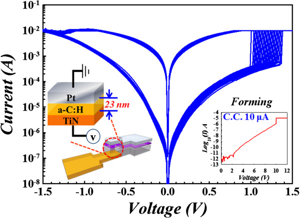
Current–voltage sweeps of Pt/a-C:H/TiN memory device.
To further evaluate the memory performance of amorphous carbon RRAM, the endurance and retention tests were shown in Figure 2. The resistance values of reliability and sizing effect measurement were obtained by a read voltage of 0.2 V. The device exhibits stable HRS and LRS even after more than 107 sweeping cycles (Figure 2a), which demonstrates its acceptable switching endurance capability. The retention characteristics of HRS and LRS at T = 85°C are shown in Figure 2b. No significant degradation of resistance in HRS and LRS was observed. It indicates that the device has good reliability for nonvolatile memory applications. Figure 2c reveals the resistance of LRS and HRS states with various sizes of via hole, which is independent with the electrode area of the device. According to the proposed model by Sawa [44], the resistive switching behavior in carbon RRAM is attributed to filament-type RRAM.
Figure 2.
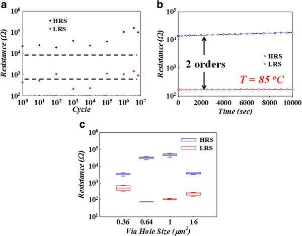
Endurance (a), retention properties (b), and sizing effect measurement (c) of Pt/a-C:H/TiN memory device.
To investigate the interesting phenomena, we utilized the material spectrum analyses to find out the reason of working current reduction and better stability. The sputtered carbon film was analyzed by Raman spectroscopy and the spectra revealed in Figure 3a. The broaden peak from 1,100 to 1,700 cm-1 demonstrates the existence of amorphous carbon structure [45].
Figure 3.
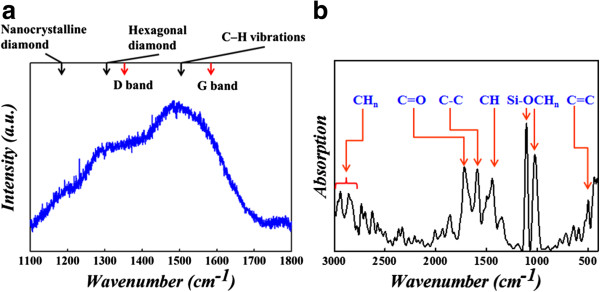
Raman spectra of C sp 2 and C sp 3 in amorphous carbon film (a); FTIR spectrum of amorphous carbon film (b).
In order to further testify the existence of the carbon layer and find its chemical bonding type, FTIR was used to analyze the sputtered carbon thin film. C-H stretch peak can be observed at the wave number of 2,800 to 3,000 cm-1, as shown in the FTIR spectra of Figure 3b.
To clarify the current transportation mechanism, the current vs. voltage (I-V) is presented in Figure 4. The LRS shows symmetric I-V curve at positive and negative electrical field. The electron transport exhibits Poole-Frenkel and Hopping conduction at middle and high voltage. However, the I-V curve is asymmetric in HRS, but the current transportation mechanism is Schottky emission and Hopping at middle and high voltage. The resistive switching mechanism of LRS and HRS is given in detail as follows.
Figure 4.
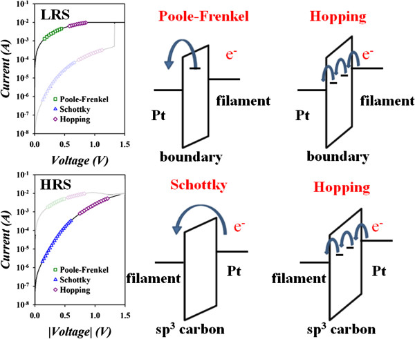
I-V curve fitting of Pt/a-C:H/TiN memory device with various carrier transport mechanisms.
On the basis of the electrical and material analyses, we proposed a reaction model to explain the transfer of carrier conduction mechanism of the amorphous carbon RRAM as shown in Figure 5. The conductive filament will be formed after the forming process, which is attributed to the connection between sp2 carbon fractions in the amorphous carbon layer [46]. Due to the current compliance, there is remaining amorphous carbon between conductive sp2 regions, as shown in left insert of Figure 5. Because the current pass through the boundaries of sp2 regions, the current fitting is dominated by Poole-Frenkel conduction in LRS. As higher voltage was applied, the significant barrier lowering caused the conduction dominated by hopping conduction through conjugation double bonds of sp2 carbon filament. When the bottom TiN electrode is applied with a negative bias to perform a reset process, hydrogen atoms were pulled from the Pt electrode and absorbed by double bonds of sp2 carbon, namely hydrogenation process. The hydrogenation reaction will transfer the conductive sp2 carbon filament into insulated sp3 carbon filament. As shown in the right insert of Figure 5, the region of filament near Pt electrode forms insulated sp3 carbon dominated, which leads to the current conduction exhibit Schottky conduction in HRS. The Hopping conduction is attributed to significant barrier lowering as the higher voltage was applied. Contrariwise, the hydrogen atoms were repelled to Pt electrode to form sp2 carbon filament during set process, called as dehydration process. Based on the hydrogen redox model, a repeatable switching behavior can be obtained in C-RRAM device.
Figure 5.
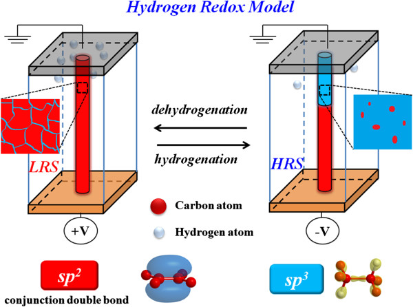
Hydrogen redox model of Pt/a-C:H/TiN memory device in LRS and HRS states.
Conclusion
In conclusion, the amorphous carbon RRAM has been fabricated to investigate the resistive switching characteristics. The device has good resistive switching properties due to hydrogenation and dehydrogenation of H atoms in carbon RRAM. The material and electrical analyses give convincing evidence of hydrogen redox induced resistance switching in amorphous carbon RRAM. The current conduction of LRS was contributed to formation of conjugation double bonds in the carbon layer after dehydrogenation. Moreover, the current conduction of HRS was dominated by insulating sp3 carbon after hydrogenation at a reverse electrical filed.
Competing interests
The authors declare that they have no competing interests.
Authors’ contributions
YJC designed and set up the experimental procedure. HLC conducted the electrical measurement of the devices. TCC and TFY planned the experiments and agreed with the paper’s publication. TMT, KCC, KHC, and JCL revised manuscript critically and make some changes. RZ fabricated the devices with the assistance of TJC. JHC performed the Raman and FTIR spectra measurement. DHB and SMS assisted in the data analysis. All authors read and approved the final manuscript.
Contributor Information
Yi-Jiun Chen, Email: chen.yijiun@gmail.com.
Hsin-Lu Chen, Email: M003020089@student.nsysu.edu.tw.
Tai-Fa Young, Email: youngtf@mail.nsysu.edu.tw.
Ting-Chang Chang, Email: tcchang@mail.phys.nsysu.edu.tw.
Tsung-Ming Tsai, Email: tmtsai@faculty.nsysu.edu.tw.
Kuan-Chang Chang, Email: doubleccc@yahoo.com.tw.
Rui Zhang, Email: 1129zhangrui@gmail.com.
Kai-Huang Chen, Email: d9131802@gmail.com.
Jen-Chung Lou, Email: jesselou@ss.pku.edu.cn.
Tian-Jian Chu, Email: Invisibleman719@hotmail.com.
Jung-Hui Chen, Email: t1446@nknucc.nknu.edu.tw.
Ding-Hua Bao, Email: stsbdh@mail.sysu.edu.cn.
Simon M Sze, Email: simonsze@faculty.nctu.edu.tw.
Acknowledgements
This work was performed at National Science Council Core Facilities Laboratory for Nano-Science and Nano-Technology in Kaohsiung-Pingtung area and supported by the National Science Council of the Republic of China under contract nos. NSC 102-2120-M-110-001 and NSC 101-2221-E-044-MY3.
References
- Guan WH, Long SB, Jia R, Liu M. Nonvolatile resistive switching memory utilizing gold nanocrystals embedded in zirconium oxide. Appl Phys Lett. 2007;9:062111. doi: 10.1063/1.2760156. [DOI] [Google Scholar]
- Liu Q, Guan WH, Long SB, Jia R, Liu M, Chen JN. Resistive switching memory effect of ZrO2 films with Zr+ implanted. Appl Phys Lett. 2008;9:012117. doi: 10.1063/1.2832660. [DOI] [Google Scholar]
- Chang TC, Jian FY, Chen SC, Tsai YT. Developments in nanocrystal memory. Mater Today. 2011;9:608–615. doi: 10.1016/S1369-7021(11)70302-9. [DOI] [Google Scholar]
- Tsai CT, Chang TC, Chen SC, Lo IK, Tsao SW, Hung MC, Chang JJ, Wu CY, Huang CY. Influence of positive bias stress on N2O plasma improved InGaZnO thin film transistor. Appl Phys Lett. 2010;9:242105. doi: 10.1063/1.3453870. [DOI] [Google Scholar]
- Chen TC, Chang TC, Tsai CT, Hsieh TY, Chen SC, Lin CS, Hung MC, Tu CH, Chang JJ, Chen PL. Behaviors of InGaZnO thin film transistor under illuminated positive gate-bias stress. Appl Phys Lett. 2010;9:112104. doi: 10.1063/1.3481676. [DOI] [Google Scholar]
- Liu J, Wang Q, Long SB, Zhang MH, Liu M. A metal/Al2O3/ZrO2/SiO2/Si (MAZOS) structure for high-performance non-volatile memory application. Semicond Sci Technol. 2010;9:055013. doi: 10.1088/0268-1242/25/5/055013. [DOI] [Google Scholar]
- Jiang DD, Zhang MH, Huo ZL, Wang Q, Liu J, Yu ZA, Yang XN, Wang Y, Zhang B, Chen JN, Liu M. A study of cycling induced degradation mechanisms in Si nanocrystal memory devices. Nanotechnology. 2011;9:254009. doi: 10.1088/0957-4484/22/25/254009. [DOI] [PubMed] [Google Scholar]
- Syu YE, Chang TC, Tsai TM, Hung YC, Chang KC, Tsai MJ, Kao MJ, Sze SM. Redox reaction switching mechanism in RRAM device with Pt/CoSiOX/TiN structure. IEEE Electron Device Lett. 2011;9:545–547. [Google Scholar]
- Chen MC, Chang TC, Tsai CT, Huang SY, Chen SC, Hu CW, Sze SM, Tsai MJ. Influence of electrode material on the resistive memory switching property of indium gallium zinc oxide thin films. Appl Phys Lett. 2010;9:262110. doi: 10.1063/1.3456379. [DOI] [Google Scholar]
- Zhu CX, Huo ZL, Xu ZG, Zhang MH, Wang Q, Liu J, Long SB, Liu M. Performance enhancement of multilevel cell nonvolatile memory by using a bandgap engineered high-κ trapping layer. Appl Phys Lett. 2010;9:253503. doi: 10.1063/1.3531559. [DOI] [Google Scholar]
- Zhu CX, Xu ZG, Huo ZL, Yang R, Zheng ZW, Cui YX, Liu J, Wang YM, Shi DX, Zhang GY, Li FH, Liu M. Investigation on interface related charge trap and loss characteristics of high-k based trapping structures by electrostatic force microscopy. Appl Phys Lett. 2011;9:223504. doi: 10.1063/1.3664222. [DOI] [Google Scholar]
- Tsai TM, Chang KC, Chang TC, Syu YE, Chuang SL, Chang GW, Liu GR, Chen MC, Huang HC, Liu SK, Tai YH, Gan DS, Yang YL, Young TF, Tseng BH, Chen KH, Tsai MJ, Ye C, Wang H, Sze SM. Bipolar resistive RAM characteristics induced by nickel incorporated into silicon oxide dielectrics for IC applications. IEEE Electron Device Lett. 2012;9:1696–1698. [Google Scholar]
- Fu D, Xie D, Feng TT, Zhang CH, Niu JB, Qian H, Liu LT. Unipolar resistive switching properties of diamondlike carbon-based RRAM devices. IEEE Electron Device Lett. 2011;9:803–805. [Google Scholar]
- Zhuge F, Dai W, He CL, Wang AY, Liu YW, Li M, Wu YH, Cui P, Li RW. Nonvolatile resistive switching memory based on amorphous carbon. Appl Phys Lett. 2010;9:163505. doi: 10.1063/1.3406121. [DOI] [Google Scholar]
- Peng PG, Xie D, Yang Y, Zhou CJ, Ma S, Feng TT, Tian H, Ren TL. Bipolar and unipolar resistive switching effects in an Al/DLC/W structure. J Phys D Appl Phys. 2012;9:365103. doi: 10.1088/0022-3727/45/36/365103. [DOI] [Google Scholar]
- Rueckes T, Kim K, Joselevich E, Tseng GY, Cheung CL, Lieber CM. Carbon nanotube-based nonvolatile random access memory for molecular computing. Science. 2000;9:94–97. doi: 10.1126/science.289.5476.94. [DOI] [PubMed] [Google Scholar]
- Wang Y, Liu Q, Long SB, Wang W, Wang Q, Zhang MH, Zhang S, Li YT, Zuo QY, Yang JH, Liu M. Investigation of resistive switching in Cu-doped HfO2 thin film for multilevel non-volatile memory applications. Nanotechnology. 2010;9:045202. doi: 10.1088/0957-4484/21/4/045202. [DOI] [PubMed] [Google Scholar]
- Kuang YB, Huang R, Ding W, Zhang LJ, Wang YG. Flexible single-component-polymer resistive memory for ultrafast and highly compatible nonvolatile memory applications. IEEE Electron Device Lett. 2010;9:758–760. [Google Scholar]
- Russo U, Ielmini D, Cagli C, Lacaita AL. Filament conduction and reset mechanism in NiO-Based Resistive-Switching Memory (RRAM) Devices. IEEE Trans Electron Devices. 2009;9:186–192. [Google Scholar]
- Standley B, Bao WZ, Zhang H, Bruck J, Lau CN, Bockrath M. Graphene-based atomic-scale switches. Nano Lett. 2008;9:3345–3349. doi: 10.1021/nl801774a. [DOI] [PubMed] [Google Scholar]
- Li YT, Long SB, Zhang MH, Liu Q, Zhang S, Wang Y, Zuo QY, Liu S, Liu M. Resistive switching properties of Au/ZrO2/Ag structure for low-voltage nonvolatile memory applications. IEEE Electron Device Lett. 2010;9:117–119. [Google Scholar]
- Sebastian A, Pauza A, Rossel C, Shelby RM, Rodríguez AF, Pozidis H, Eleftheriou E. Resistance switching at the nanometre scale in amorphous carbon. New J Phys. 2011;9:013020. doi: 10.1088/1367-2630/13/1/013020. [DOI] [Google Scholar]
- Chang KC, Tsai TM, Zhang R, Chang TC, Chen KH, Chen JH, Young TF, Lou JC, Chu TJ, Shih CC, Pan JH, Su YT, Syu YE, Tung CW, Chen MC, Wu JJ, Hu Y, Sze SM. Electrical conduction mechanism of Zn:SiOx resistance random access memory with supercritical CO2 fluid process. Appl Phys Lett. 2013;9:083509. doi: 10.1063/1.4819162. [DOI] [Google Scholar]
- Chang KC, Zhang R, Chang TC, Tsai TM, Lou JC, Chen JH, Young TF, Chen MC, Yang YL, Pan YC, Chang GW, Chu TJ, Shih CC, Chen JY, Pan CH, Su YT, Syu YE, Tai YH, Sze SM. Origin of hopping conduction in graphene-oxide-doped silicon oxide resistance random access memory devices. IEEE Electron Device Lett. 2013;9:677–679. [Google Scholar]
- Zhang R, Chang KC, Chang TC, Tsai TM, Chen KH, Lou JC, Chen JH, Young TF, Shih CC, Yang YL, Pan YC, Chu TJ, Huang SY, Pan CH, Su YT, Syu YE, Sze SM. High performance of graphene oxide-doped silicon oxide-based resistance random access memory. Nanoscale Res Lett. 2013;9:497. doi: 10.1186/1556-276X-8-497. [DOI] [PMC free article] [PubMed] [Google Scholar]
- Tsai TM, Chang KC, Zhang R, Chang TC, Lou JC, Chen JH, Young TF, Tseng BH, Shih CC, Pan YC, Chen MC, Pan JH, Syu YE, Sze SM. Performance and characteristics of double layer porous silicon oxide resistance random access memory. Appl Phys Lett. 2013;9:253509. doi: 10.1063/1.4812474. [DOI] [Google Scholar]
- Chang KC, Pan CH, Chang TC, Tsai TM, Zhang R, Lou JC, Young TF, Chen JH, Shih CC, Chu TJ, Chen JY, Su YT, Jiang JP, Chen KH, Huang HC, Syu YE, Gan DS, Sze SM. Hopping effect of hydrogen-doped silicon oxide insert RRAM by supercritical CO2 fluid treatment. IEEE Electron Device Lett. 2013;9:617–619. [Google Scholar]
- Chang KC, Tsai TM, Chang TC, Wu HH, Chen KH, Chen JH, Young TF, Chu TJ, Chen JY, Pan CH, Su YT, Syu YE, Tung CW, Chang GW, Chen MC, Huang HC, Tai YH, Gan DS, Wu JJ, Hu Y, Sze SM. Low temperature improvement method on Zn:SiOx resistive random access memory devices. IEEE Electron Device Lett. 2013;9:511–513. [Google Scholar]
- Chang KC, Tsai TM, Chang TC, Wu HH, Chen JH, Syu YE, Chang GW, Chu TJ, Liu GR, Su YT, Chen MC, Pan JH, Chen JY, Tung CW, Huang HC, Tai YH, Gan DS, Sze SM. Characteristics and mechanisms of silicon-oxide-based resistance random access memory. IEEE Electron Device Lett. 2013;9:399–401. [Google Scholar]
- Tsai TM, Chang KC, Chang TC, Chang GW, Syu YE, Su YT, Liu GR, Liao KH, Chen MC, Huang HC, Tai YH, Gan DS, Ye C, Wang H, Sze SM. Origin of hopping conduction in Sn-doped silicon oxide RRAM with supercritical CO2 fluid treatment. IEEE Electron Device Lett. 2012;9:1693–1695. [Google Scholar]
- Tsai TM, Chang KC, Chang TC, Syu YE, Liao KH, Tseng BH, Sze SM. Dehydroxyl effect of Sn-doped silicon oxide resistance random access memory with supercritical CO2 fluid treatment. Appl Phys Lett. 2012;9:112906. doi: 10.1063/1.4750235. [DOI] [Google Scholar]
- Chang KC, Huang JW, Chang TC, Tsai TM, Chen KH, Young TF, Chen JH, Zhang R, Lou JC, Huang SY, Pan YC, Huang HC, Syu YE, Gan DS, Bao DH, Sze SM. Space electric field concentrated effect for Zr:SiO2 RRAM devices using porous SiO2 buffer layer. Nanoscale Res Lett. 2013;9:523. doi: 10.1186/1556-276X-8-523. [DOI] [PMC free article] [PubMed] [Google Scholar]
- Chang KC, Tsai TM, Chang TC, Syu YE, Chuang SL, Li CH, Gan DS, Sze SM. The effect of silicon oxide based RRAM with tin doping. Electrochem Solid-State Lett. 2012;9:H65–H68. doi: 10.1149/2.013203esl. [DOI] [Google Scholar]
- Chang KC, Tsai TM, Chang TC, Syu YE, Wang CC, Chuang SL, Li CH, Gan DS, Sze SM. Reducing operation current of Ni-doped silicon oxide resistance random access memory by supercritical CO2 fluid treatment. Appl Phys Lett. 2011;9:263501. doi: 10.1063/1.3671991. [DOI] [Google Scholar]
- Syu YE, Chang TC, Tsai TM, Chang GW, Chang KC, Lou JH, Tai YH, Tsai MJ, Wang YL, Sze SM. Asymmetric carrier conduction mechanism by tip electric field in WSiOX resistance switching device. IEEE Electron Device Lett. 2012;9(3):342–344. [Google Scholar]
- Long SB, Perniola L, Cagli C, Buckley J, Lian XJ, Miranda E, Pan F, Liu M, Sune J. Voltage and power-controlled regimes in the progressive uni-polar RESET transition of HfO2-based RRAM. Sci Rep. 2013;9:2929. doi: 10.1038/srep02929. [DOI] [PMC free article] [PubMed] [Google Scholar]
- Syu YE, Chang TC, Lou JH, Tsai TM, Chang KC, Tsai MJ, Wang YL, Liu M, Sze SM. Atomic-level quantized reaction of HfOx memristor. Appl Phys Lett. 2013;9:172903. doi: 10.1063/1.4802821. [DOI] [Google Scholar]
- Long SB, Lian XJ, Cagli C, Perniola L, Miranda E, Liu M, Sune J. A model for the set statistics of RRAM inspired in the percolation model of oxide breakdown. IEEE Electron Device Lett. 2013;9(8):999–1001. [Google Scholar]
- Chu TJ, Chang TC, Tsai TM, Wu HH, Chen JH, Chang KC, Young TF, Chen KH, Syu YE, Chang GW, Chang YF, Chen MC, Lou JH, Pan JH, Chen JY, Tai YH, Ye C, Wang H, Sze SM. Charge quantity influence on resistance switching characteristic during forming process. IEEE Electron Device Lett. 2013;9(4):502–504. [Google Scholar]
- Long SB, Lian XJ, Cagli C, Cartoixa X, Rurali R, Miranda E, Jimenez D, Perniola L, Liu M, Sune J. Quantum-size effects in hafnium-oxide resistive switching. Appl Phys Lett. 2013;9(18):183505. doi: 10.1063/1.4802265. [DOI] [Google Scholar]
- Su YT, Chang KC, Chang TC, Tsai TM, Zhang R, Lou JC, Chen JH, Young TF, Chen KH, Tseng BH, Shih CC, Yang YL, Chen MC, Chu TJ, Pan CH, Syu YE, Sze SM. Characteristics of hafnium oxide resistance random access memory with different setting compliance current. Appl Phys Lett. 2013;9(16):163502. doi: 10.1063/1.4825104. [DOI] [Google Scholar]
- Zhang R, Tsai TM, Chang TC, Chang KC, Chen KH, Lou JC, Young TF, Chen JH, Huang SY, Chen MC, Shih CC, Chen HL, Pan JH, Tung CW, Syu YE, Sze SM. Mechanism of power consumption inhibitive multi-layer Zn:SiO2/SiO2 structure resistance random access memory. J. 2013;9:234501. doi: 10.1063/1.4843695. [DOI] [Google Scholar]
- Chang KC, Chen JH, Tsai TM, Chang TC, Huang SY, Zhang R, Chen KH, Syu YE, Chang GW, Chu TJ, Liu GR, Su YT, Chen MC, Pan JH, Liao KH, Tai YH, Young TF, Sze SM, Ai CF, Wang MC, Huang JW. Improvement mechanism of resistance random access memory with supercritical CO2 fluid treatment. J. of Supercritical Fluids. 2014;9:183–189. [Google Scholar]
- Sawa A. Resistive switching in transition metal oxides. Mater Today. 2008;9:28–36. [Google Scholar]
- Schwan J, Ulrich S, Batori V, Ehrhardt H, Silva SRP. Raman spectroscopy on amorphous carbon films. J Appl Phys. 1996;9:440–447. doi: 10.1063/1.362745. [DOI] [Google Scholar]
- Evtukh A, Litovchenko V, Semenenko M, Yilmazoglu O, Mutamba K, Hartnagel HL, Pavlidis D. Formation of conducting nanochannels in diamond-like carbon films. Semicond Sci Technol. 2006;9:1326–1330. doi: 10.1088/0268-1242/21/9/018. [DOI] [Google Scholar]


