

Abstract
X-ray Photoelectron Spectroscopy (XPS) was used to characterize the nitrogen species in perfluorophenylazide (PFPA) self-assembled monolayers. PFPA chemistry is a novel immobilization method for tailoring the surface properties of materials. It is a simple route for the efficient immobilization of graphene, proteins, carbohydrates and synthetic polymers onto a variety of surfaces. Upon light irradiation, the azido group in PFPA is converted to a highly reactive singlet nitrene species that readily undergoes CH insertion and C=C addition reactions. Here, the challenge of characterizing the PFPA modified surfaces was addressed by detailed XPS experimental analyses. The three nitrogen peaks detected in the XPS N1s spectra were assigned to amine/amide (400.5 eV) and azide (402.1 and 405.6 eV) species. The observed 2:1 ratio of the areas from the 402.1 eV to 405.6 eV peaks suggests the assignment of the peak at 402.1 eV to the two outer nitrogen atoms in the azido group and assignment of the peak at 405.6 eV to the central nitrogen atom in the azido group. The azide decomposition as the function of x-ray exposure was also determined. Finally, XPS analyses were conducted on patterned graphene to investigate the covalent bond formation between the PFPA and graphene. This study provides strong evidence for the formation of covalent bonds during the PFPA photocoupling process.
Keywords: PFPA, XPS, Surface Characterization, Graphene
Introduction
The surface structure and composition of materials determine their properties and performance, therefore, tailoring the surface properties of a material through surface modification is an important method to control the function of materials.1–8 Self-assembled monolayers (SAMs) have become an excellent technique for the modification and functionalization of a variety of surfaces.3,4,9–11 Azide-terminated SAMs provide an excellent route for thin films fabrication and allow tailoring surface properties through covalent immobilization.9–11 The most common uses of azides are the click chemistry12–20 and photochemistry21,22. Recently, perfluorophenyl azides (PFPAs) have been developed to introduce functional groups onto solid surfaces.23–25 Upon light or thermal activation, the azido group in the PFPA structure is converted to a highly reactive nitrene species that readily inserts into CH and NH bonds or undergoes cycloaddition reaction with C=C bonds.23,26,27 This bimolecular reaction, which is much less efficient in alkyl azides or phenyl azides,28–31 makes PFPAs highly efficient in surface functionalization. The functionalization process is simple and reproducible, and has been proven to be efficient for the immobilization of graphene, proteins and other small biomolecules, carbohydrates and synthetic polymers onto surfaces.23,32–38 Moreover, the surface density of immobilized molecules can be controlled through the PFPA concentration.33,39 The PFPA chemistry has been used to globally modify surfaces or to modify discrete areas by arraying techniques such as photomasking or printing devices.40
In this work, X-ray Photoelectron Spectroscopy (XPS) was used to study in detail the nitrogen species present in PFPA-functionalized surfaces (PFPA-silane SAMs on silicon wafers as well as PFPA-thiol SAMs on gold slides). XPS is a surface analysis technique that is a highly sensitive tool for determining the surface chemical properties such as quantitative surface elemental compositions (compositional scans), chemical environment of different elements (high resolution scans) and lateral distribution of elements on the surface (imaging).41 XPS has been used to study the azide and the chemical environment around the nitrogen atoms in particular.15–17,42–44 In this paper, we conducted comprehensive studies of the PFPA-functionalized surface including a series of reference studies to achieve an in-depth understanding of XPS characteristics of the PFPA surfaces. Our XPS study of the nitrogen peak provides a detailed and accurate peak assignment of its different chemical states. The PFPA-surface was subsequently used to covalently immobilize graphene by photolithography. XPS provided evidence of the covalent bond formation between PFPA and graphene. Furthermore, XPS imaging was used to characterize the elemental lateral distribution on the surface and to verify the graphene patterns on the surface.
Materials and Methods
Materials
Zinc powder was purchased from Sigma-Aldrich. Toluene, chloroform, dichloromethane, o-dichlorobenzene (DCB) and ethanol were purchased from Fisher. Silicon wafers having an oxide layer thickness of ~275 nm were purchased from Silicon Valley Microelectronics, Inc. (Santa Clara, CA). N-(3-Trimethoxysilylpropyl)-4-azido-2,3,5,6-tetrafluorobenzamide (PFPA-silane),45 N-(3-trimethoxysilylpropyl)-2,3,4,5,6-pentafluorobenzamide (PFB-silane),39 and 11,11′-disulfanediylbis(undecane-11,1-diyl)bis(4-azido-2,3,5,6-tetrafluorobenzoate) (PFPA-disulfide)42 (Figure 1) were synthesized following previously reported procedures.
Figure 1.

Molecular structures of PFPA-silane, PFB-silane, PFPA-disulfide, ATFP-thiol.
1H and 13C NMR data were recorded on a Bruker AMX-400 MHz spectrometer. Chemical shifts are reported as δ values (ppm) with CDCl3 (1H = 7.26, 13C = 77.16) as the internal standard. FTIR analysis was performed on a Nicolet iS10 spectrophotometer using a diamond attenuated total reflectance (ATR) attachment.
Synthesis of 11-mercaptoundecyl 4-amino-2,3,5,6-tetrafluorobenzoate (ATFP-thiol)
PFPA-disulfide (20 mg) was dissolved in ethanol (20 mL), and concentrated HCl (37%, 1.0 mL) and zinc dust (1.0 g) were added into the solution. The reaction mixture was stirred vigorously overnight at room temperature, filtered, and the solvent was removed from the filtrate by rotary evaporation. The residue was re-dissolved in chloroform, washed first with dilute Na2CO3 solution and then with water, and finally dried over anhydrous Na2SO4. The crude product was purified by silica gel column chromatography to give ATFP-thiol (Figure 1) as a colorless oil (12.0 mg, 64%). 1H NMR (CDCl3): δ (ppm) 4.31 (t and br, 4H), 2.52 (q, J = 7.6 Hz, 2H), 1.73 (m, 2H), 1.61 (m, 2H), 1.43-1.35 (m, 15H). 13C NMR (CDCl3): δ (ppm) 160.8, 142 (d, JC-F = 254 Hz), 140 (d, JC-F = 248 Hz), 129.6, 99.6, 65.9, 34.1, 29.4-25.8, 24.6. FTIR (ATR): 3505, 3369, 2921, 2851, 1707, 1647, 1593, 1532, 1505, 1409, 1309, 1251 cm−1.
Preparation of PFPA-functionalized substrates
Silicon wafers were cleaned with piranha solution (7:3 v/v conc. H2SO4/35 wt% H2O2) (Caution: the piranha solution reacts vigorously with organic materials and solvents.), followed by thorough washing with boiling water and dried under flowing nitrogen. The wafer was then incubated in a solution of PFPA-silane, PFB-silane (Figure 1) or a mixture of the two silanes in toluene for 4 h at room temperature in a sealed vial. The concentration of the silane or the mixed silanes was kept at 12.6 mM. This process was carried out in sealed vials to minimize contact with moisture in the air. The treated wafers were rinsed with toluene, dried under flowing nitrogen, and cured at room temperature for 24 h.
Gold slides were prepared by coating piranha-cleaned glass slides with a 2 nm thick titanium film followed by a 200 nm thick gold film in an electron beam evaporator (CrC-100 Sputtering System, Plasma Sciences Inc., Lorton, VA). Before each experiment, the gold slides were cleaned with the piranha solution for 1 min, washed thoroughly 3 times with boiling water for 30 min each, and dried under a stream of nitrogen. Cleaned slides were then soaked in a solution of PFPA-disulfide or ATFP-thiol (Figure 1) in chloroform (10 mM) for 24 h. The slides were rinsed gently with chloroform and dried under nitrogen.
Fabrication of graphene patterns
The patterns were fabricated as previously reported.40 Briefly, graphite flakes (50 mg, Sigma) were added to DCB (20 mL) and the mixture was sonicated using a sonication probe (SONICS, VCX130) for 1 h and settled for 1 week. The supernatant of the mixture was then centrifuged at 4500 rpm for 30 min. The upper solution was collected and was deposited onto PFPA-functionalized wafer by spin-coating at 1000 rpm for 2 min or by drop-coating followed by drying under vacuum. A photomask was placed on top of the graphene-coated wafer, and irradiated under ambient conditions with a 450-W medium pressure Hg lamp (Hanovia) for 10 min in the presence of a 280-nm optical filter. The lamp reached its full power of 5.0 mW/cm2 after a 2 min warm-up, as measured by a model UVX radiometer and UVX-36 sensor (Upland, CA). The power after the light had passed through the filter was measured at 2.4 mW/cm2. Samples were then sonicated in DCB followed by washing with DCB and ethanol, and dried.
X-ray Photoelectron Spectroscopy
XPS measurements were performed on a Kratos Axis Ultra DLD instrument (Kratos, Manchester, England) employing a hemispherical analyzer for spectroscopy and a spherical mirror analyzer for imaging. Spectra and images were acquired with a monochromated Al Kα X-ray source and a 0° takeoff angle (TOA). The TOA is defined as the angle between the sample surface normal and the axis of the XPS analyzer lens. Pressure in the analytical chamber during spectral acquisition was less than 5×10⁻⁹ Torr. High-resolution spectra were acquired at 700 μm × 300 μm field of view with an analyzer pass energy of 20 eV and composition spectra were acquired with an analyzer pass energy of 80 eV. Binding energies (BEs) were referenced to the hydrocarbon C1s peak at 285 eV. Three spots on two or more replicates of each sample type were analyzed. The compositional data are an average of the values determined at each spot. Parallel images were acquired at 400 μm × 400 μm field of views with an analyzer pass energy of 160 eV. Background region images were taken at a binding energy that was 15 eV below each relevant peak and corrected images were obtained by subtraction of the background region image from the image at the peak of interest. Compositional analyses of the images (small spot analyses) were performed by collecting small area region of interest (ROI) scans (27 μm diameter spot). These small spot compositional survey scans were acquired using an anayzer pass energy of 160 eV. Data analyses were performed with CasaXPS.
Results and discussion
Various SAMs were prepared by treating silicon wafers or gold slides with a solution of PFPA-silane or PFB-silane in toluene, or PFPA-disulfide or ATFP-thiol in chloroform (Figure 1). The XPS-determined elemental compositions for the different SAMs are shown in Table 1. As expected, all samples contain nitrogen, fluorine, carbon and oxygen. XPS also detected silicon from the silane-functionalized wafer, and gold and sulfur from the disulfide- and thiol-functionalized gold. All SAMs have an aliphatic chain and a perfluorophenyl head group, and therefore, the fluorine-to-carbon ratios are a good indication to the SAMs quality. For the PFPA-silane SAM, the XPS determined fluorine-to-carbon atomic ratio is 0.4 (Table 1), which is in agreement with the stoichiometric value of 0.4 expected for the PFPA-silane molecule after the loss of all three methoxy groups from the silanization process. For the PFB-silane SAM, the fluorine-to-carbon atomic ratio in Table 1 is 0.62 versus the stoichiometric value of 0.5, the higher experimental value suggests that the PFB-silane SAM is denser and as a result the carbon signal is attenuated by the fluorine atoms. For the PFPA-silane:PFB-silane mixed SAM, the fluorine-to-carbon atomic ratio in Table 1 is 0.53, and as expected, this value is between the experimental values of the two pure SAMs. The XPS determined fluorine-to-carbon atomic ratio of the SAM from PFPA-disulfide is 0.2 (versus the stoichiometric value of 0.22). The XPS determined and stoichiometric values of the fluorine-to-carbon ratio for the SAM from ATFP-thiol are both 0.22.
Table 1.
XPS elemental composition of PFPA-silane SAM, a 1:10 mixed SAM of PFPA-silane and PFB-silane, PFB-silane SAM, PFPA-disulfide SAM, and ATFP-thiol SAM.
| Atomic % | F/C | ||||||||
|---|---|---|---|---|---|---|---|---|---|
| N1s | F1s | O1s | C1s | Si2p | S2p | Au4f | XPS | stoichiometric value (theoretical) | |
| PFPA-silane SAM | 7.4±0.1 | 9.9±0.1 | 38.1±2.2 | 24.7±1.8 | 19.8±0.3 | --- | --- | 0.4 | 0.4 |
| PFPA-silane:PFB-silane (1:10) SAM | 2.4±0.3 | 14.7±0.3 | 34.9±0.3 | 27.8±1.1 | 20.2±0.6 | --- | --- | 0.53 | 0.4–0.5 |
| PFB-silane SAM | 2.3±0.1 | 15.7±0.2 | 36.9±0.7 | 25.5±0.5 | 19.6±0.1 | --- | --- | 0.62 | 0.5 |
| PFPA-disulfide SAM | 4.7±1.1 | 8.2±0.2 | 7.7±1.7 | 41.7±1.9 | --- | 1.9±0.1 | 35.7±1.1 | 0.2 | 0.22 |
| ATFP-thiol SAM | 3.7±0.1 | 10.5±0.2 | 9.3 ±0.7 | 47.3±0.4 | --- | 1.2±0.2 | 27.9±0.5 | 0.22 | 0.22 |
The fluorine-to-nitrogen atomic ratios also vary significantly among the four different SAMs. Based on the molecular stoichiometry, the values are expected to increase in the following order: PFPA-silane (1) < PFPA-disulfide (1.3) < ATFP-thiol (4) < PFB-silane (5). The same rank order was observed in the experimentally determined fluorine-to-nitrogen atomic ratios. The XPS determined fluorine-to-nitrogen atomic ratio for the mixed SAM of PFPA-silane:PFB-silane was between the values for the two pure SAMs, as expected.
The C1s high-resolution XPS peaks from the SAMs on silicon wafer (Figure 2, a and b) were fit into three components at 285.0 (C=C-C and C-H), 286.6 (C=C-N and C-N) and 288.2 eV (C=C–F and O=C-N). The C1s high-resolution XPS peaks from the SAMs on gold (Figure 2, c and d) were fit into four components at 285.0 (C=C-C and C-H), 286.6 (C=C-N and C-O), 287.8–288.2 eV (C=C–F) and an additional peak at 289.5 eV (O=C-O). These species are all expected from the molecular structures of the studied SAMs.
Figure 2.

High-resolution XPS C1s core level spectra of (a) PFPA-silane or (b) PFB-silane functionalized silicon wafers, and (c) PFPA-disulfide or (d) ATFP-thiol functionalized gold surfaces. The different peaks in each fit and their binding energies are provided in table 2.
The PFPA chemistry is primarily that of the azido (-N3) group, and studying the nature of the nitrogen species is therefore essential in understanding the PFPA characteristics. Figure 3a shows the high-resolution XPS N1s spectrum of the PFPA-silane-functionalized wafer. This spectrum exhibited three peaks at 400.5, 402.1, and 405.6 eV (Table 3). An accurate peak assignment was the first goal of this study and was achieved by examining three reference samples: a silicon wafer functionalized with PFB-silane (Figure 3b), gold surfaces functionalized with PFPA-disulfide (Figure 4a) and ATFP-thiol (Figure 4b).
Figure 3.

High-resolution XPS N1s core level spectra of (a) PFPA-silane or (b) PFB-silane functionalized silicon wafers.
Table 3.
XPS N1s peak area ratios for various surfaces.
| BE | 400.5 eV | 402.1 eV | 405.6 eV |
|---|---|---|---|
| FWHM | 1.4 | 1.4 | 1.4 |
| PFPA-silane SAM | 0.41 | 0.41 | 0.18 |
| PFPA-silane:PFB-silane (10:1) SAM | 0.84 | 0.16 | -- |
| PFB-silane SAM | 1.0 | -- | -- |
| PFPA-disulfide SAM | -- | 0.68 | 0.32 |
| ATFP-thiol SAM | 1.0 | -- | -- |
Figure 4.

High-resolution XPS N1s core level spectra of (a) PFPA-disulfide and (b) ATFP-thiol functionalized gold surfaces.
The PFB-silane SAM (Figure 3b) and ATFP-thiol SAM (Figure 4b) have only one N species in their structures, an amide in PFB-silane and an amine in ATFP-thiol. The XPS N1s core level spectra from these two SAMs contain only a single nitrogen peak, both located at 400.5 eV. The PFPA-disulfide SAM (Figure 4a) has the azide structure but no amide N atom, and shows only the two higher BE peaks (402.1 and 405.6 eV). Thus, the two higher BE peaks in the PFPA-silane SAM (Figure 3a) can be assigned to the N atoms in the azide structure and the lowest BE (400.5 eV) of the three N peaks in PFPA can be attributed to the amide N. Further evidence for these peak assignments was obtained by examining mixtures that contained different ratios of PFPA and PFB. For example, the functionalized wafer with a 1:10 mixture of PFPA-silane and PFB-silane has two nitrogen peaks, Figure S1 (Supporting Information): the amide peak at 400.5 eV and another small peak at 402.1 eV. The peak at 405.6 eV is below the limit of detection for PFPA-silane:PFB-silane mixed SAM due to the low surface density of PFPA-silane and therefore is not observed in the N1s spectra collected from this surface. This observation is consistent with highest BE peaks being attributed to the N atoms in the azide structure.
The observed ratio of the two nitrogen peaks for the three N atoms of the azido group in the PFPA-disulfide SAM is 2:1, which can be explained by the resonance structures shown in Figure 5. The N atoms marked a and c in Figure 5, Na and Nc, have equal chance to bear a negative charge and each can be assigned a formal charge of −0.5. Although Nc is directly attached to a fluorinated phenyl group, the BE shift induced by the fluorinated phenyl group is too small to differentiate, and therefore the peak at 402.1 eV was assigned to both Na and Nc. The middle N atom, Nb in Figure 5, has a formal charge of +1 and contributes to the highest BE peak at 405.6 eV.
Figure 5.
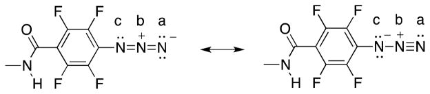
The resonance structures of PFPA illustrating how the N(a) and N(c) atoms are equivalent but the N(b) atom differs, in agreement with the 2:1 peak area ratio observed in the XPS high resolution N 1s spectra.
The azido group on the PFPA-silane SAM also has the two higher BE nitrogen peaks with a 2:1 ratio, but the lower BE peak at 400.5 eV is twice the area expected from the stoichiometric composition of the PFPA-silane molecule. Since the azido group is labile when exposed to irradiation or heat, possibility exists that partial decomposition occurs due to exposure of this reactive group to X-rays during the XPS analysis.47 To test this hypothesis, PFPA samples were subjected to X-ray irradiation and the N1s spectra were collected at varying exposure times. Figure 6 presents the ratio for each of the three N1s components to the total nitrogen peak area for the PFPA-silane SAM as a function of X-ray exposure time. The peak ratios for all three nitrogen species change significantly with X-ray exposure time. For example, after a 30 min exposure, the peak at 405.6 eV decreased to 25% of its initial value. The peak at 402.1 eV also decreased at the same rate as the peak at 405.6 eV. On the contrary, the fraction of the C-N component at 400.5 eV increases at twice the rate upon exposure to X-ray irradiation. This suggests that the Nc–Nb bond of the azido group is unstable under the XPS mesurement environment. The higher percentage of nitrogen species at 400.5 eV could be attributed to the azide decomposition products including derivatives of azirine or azacycloheptatetraene.33
Figure 6.

Change in high-resolution XPS N 1s peak area ratio during exposure of the PFPA–silane functionalized silicon wafer to monochromatized 1486.6 eV X-ray irradiation: relative area of the three N1s peaks to the entire N1s signal (● 400.5 eV peak, ■ 402.1 eV peak, ▲ 405.6 eV peak).
Azide chemistry in general and PFPA chemistry in particular is convenient for modifying surfaces through immobilization of graphene, polymers and carbohydrates.39,48,49 In this work, patterned graphene was used as an example as it has an ongoing interest in the area of fabricating graphene-based nanomaterials, devices, and sensors.40,50–52 For C1s, after the graphene immobilization, the peak intensity at 285.0 eV (C-C/C-H) increased drastically whereas the other two carbon peaks decreased, Figure S2 (Supporting Information). Figure 7 shows the high-resolution XPS N1s spectra of immobilized graphene on the PFPA-functionalized silicon wafer and PFPA-functionalized gold. These spectra were acquired after the same UV exposures and they exhibited only two components, which were fit to two peaks at 400.5 eV and 402.1 eV, respectively. The ratios between the peaks at 400.5 eV and 402.1 eV are 1.9 for the immobilized graphene on the PFPA-functionalized silicon and 1.5 for the immobilized graphene on the PFPA-functionalized gold. The higher ratio for the immobilized graphene on the PFPA-functionalized silicon is expected considering the amide N present in the PFPA-silane molecule which also has peak at 400.5 eV. The small bump at around 406 eV in Figure 7a is due to traces of unreacted azides. Figure S3 (Supporting Information) shows the high-resolution XPS N1s core level spectrum of PFPA-functionalized gold surface that was exposed to UV irradiation in the absence of graphene, which was also fit to two peaks at 400.5 eV and 402.1 eV. On this spectrum the ratio between the peaks at 400.5 eV and 402.1 eV is 2.8. The fact that the peak at 402.1 eV is smaller in case of UV irradiation in the absence of graphene suggest that this peak should result from the N in the covalent adducts that form after the nitrene reacted with the graphene overlayer. In a recent work where PFPA-functionalized gold surface was used to immobilize primary amines,53 the N1s XPS spectrum had only one peak at the lower binding energy around 400 eV. In our case of graphene, the cycloaddition product of azirine is proposed as the major product, however, it is difficult to assign the precise product structures by the XPS analysis alone since many N-containing species have similar binding energies. Nevertheless, it can be said with confidence that the high-resolution N1s spectra in figure 7 are consistent with covalent attachment of the graphene.
Figure 7.

High-resolution XPS N1s core level spectra of graphene attached to (a) PFPA-functionalized silicon wafer surface, and (b) PFPA-functionalized gold surface.
Additionally, XPS imaging combined with small-spot ROI analysis was used to provide quantitative surface composition of the patterned surface.54 Figure 8 shows the background subtracted XPS elemental images (Si, F, C) of the patterned graphene on silicon wafer, and Figure S4 (Supporting Information) shows the XPS elemental images (Au, C) of the patterned graphene on gold. In Figure 8, the background corrected C1s show higher signal intensity in the areas covered with graphene (lighter regions in the image). Si and F are presented in the substrate and PFPA, respectively, and lower signal intensities of these two elements are also observed in the areas covered with graphene. In Figure S4 (Supporting Information), background corrected C1s shows higher signal intensity in the areas covered with graphene, and lower Au4f intensity (which is present in the substrate) is observed in the areas covered with graphene. It was reported elsewhere40 that the thicknesses of graphene measured with AFM in the patterned areas are between ~4nm (corresponding to a mixture of 4–6 layers) and ~10–20 nm (thin graphite layer). To further determine the elemental composition of an individual spot of printed graphene, small-spot ROI analyses were performed. Consistent with XPS elemental images, as well as previous observation of the patterned graphene on the silicon substrate,40 regions that were covered with graphene show higher percentage of carbon and lower percentages of silicon, fluorine and nitrogen (Table 4). To the best of our knowledge, this is the first time that XPS is reported to define elemental lateral distribution of patterned graphene.
Figure 8.

XPS background corrected images of patterned graphene on a PFPA-functionalized silicon wafer: (a) F1s image, (b) C1s image, (c) Si2p image, (d) a superposition of all three elements (C: green, Si and F: purple). Image size: 400 μm × 400 μm. Spots marked i and ii are the areas selected for small spot analyses (see Table 4).
Table 4.
XPS determined surface elemental compositions of Spot i (substrate and PFPA) and Spot ii (graphene) in Figure 8d obtained by small-spot ROI analysis (27 μm × 27 μm).
| Atomic % | ||
|---|---|---|
| Spot i | Spot ii | |
| F 1s | 7.7 | 5.1 |
| O 1s | 28.3 | 23.2 |
| N 1s | 5.2 | 4.1 |
| Si 2p | 13.5 | 10.0 |
| C 1s | 45.3 | 57.6 |
Conclusions
This study provides a detailed characterization of the nitrogen species in PFPA SAMs before and after photoactivation and covalent attachment of patterned graphene. Using model SAMs and the experimental XPS data, the three nitrogen peaks are assigned to amine/amide (400.5 eV) and azide (402.1 and 405.6 eV) species, respectively. The 2:1 ratio of the 402.1 eV to 405.6 eV peak areas suggests the assignment of the peak at 402.1 eV to the two outer nitrogen atoms in the azido group and the assignment of the peak at 405.6 eV to the central nitrogen atom in the azido group. After photoactivation and graphene immobilization, both the carbon and the nitrogen spectra indicate covalent attachment of the graphene, although the detailed product analysis warrants further investigation by employing additional chemical and analytical methods. XPS imaging provides the lateral distribution of the elements and shows that a patterned graphene surface is formed. This work represents an important advance in the application of XPS as an essential analytical tool to elucidate the detailed chemical structure of PFPA-functionalized surfaces.
Supplementary Material
Table 2.
XPS C1s peak area ratios for various surfaces, the peaks are shown in figure 2 and the peak for PFPA-silane:PFB-silane (1:10) SAM is shown in figure S1.
| BE | 285.0 eV | 286.6 eV | 287.8–288.2 eV | 289.5 eV | |
|---|---|---|---|---|---|
| C=C-C;C-H | C=C-N; C-N; C-O | C=C-F; O=C-N | O=C-O | ||
| FWHM for silane SAMs | 1.4 | 1.4 | 1.4 | --- | |
| PFPA-silane SAM | 0.30 | 0.23 | 0.47 | --- | |
| PFPA-silane:PFB-silane (1:10) SAM | 0.22 | 0.25 | 0.53 | --- | |
| PFB-silane SAM | 0.27 | 0.22 | 0.51 | --- | |
| PFPA-disulfide SAM | FWHM | 1.1 | 1.3 | 1.3 | 1.3 |
| ratio | 0.49 | 0.18 | 0.28 | 0.05 | |
| ATFP-thiol SAM | FWHM | 1.1 | 1.3 | 1.4 | 1.3 |
| ratio | 0.44 | 0.13 | 0.35 | 0.08 | |
Acknowledgments
This research was funded by NIH grants 2R15GM066279 R01GM080295 (to M.Y.), and R01GM080295S1 and P41EB002027 (to D.G.C.).
Footnotes
Notes:
The authors declare no competing financial interest.
Supporting Information Available: High-resolution XPS N1s core level spectrum of a silicon wafer functionalized with a 1:10 mixture of PFPA-silane:PFB-silane, Figure S1; High-resolution XPS C1s core level spectrum of graphene attached to PFPA-functionalized silicon wafer surface, Figure S2; High-resolution XPS N1s core level spectrum of PFPA-functionalized gold surface that was exposed to UV irradiation in the absence of graphene, Figure S3 and XPS background corrected images of patterned graphene on a PFPA-functionalized gold, Figure S4. This information is available free of charge via the Internet at http://pubs.acs.org
References
- 1.Craighead HG. Nanoelectromechanical Systems. Science. 2000;290:1532–1535. doi: 10.1126/science.290.5496.1532. [DOI] [PubMed] [Google Scholar]
- 2.Stewart MP, Buriak JM. Chemical and Biological Applications of Porous Silicon Technology. Adv Mater. 2000;12:859–869. [Google Scholar]
- 3.Ulman A. Formation and Structure of Self-Assembled Monolayers. Chem Rev. 1996;96:1533–1554. doi: 10.1021/cr9502357. [DOI] [PubMed] [Google Scholar]
- 4.Love JC, Estroff LA, Kriebel JK, Nuzzo RG, Whitesides GM. Self-Assembled Monolayers of Thiolates on Metals as a Form of Nanotechnology. Chem Rev. 2005;105:1103–1169. doi: 10.1021/cr0300789. [DOI] [PubMed] [Google Scholar]
- 5.Smith RK, Lewis PA, Weiss PS. Patterning Self-Assembled Monolayers. Prog Surf Sci. 2004;75:1–68. [Google Scholar]
- 6.Ariga K, Hill JP, Lee MV, Vinu A, Charvet R, Acharya S. Challenges and Breakthroughs in Recent Research on Self-Assembly. Sci Technol Adv Mater. 2008;9:014109, 1–96. doi: 10.1088/1468-6996/9/1/014109. [DOI] [PMC free article] [PubMed] [Google Scholar]
- 7.Onclin S, Ravoo BJ, Reinhoudt DN. Engineering Silicon Oxide Surfaces Using Self Assembled Monolayers. Angew Chem Int Ed. 2005;44:6282–6304. doi: 10.1002/anie.200500633. [DOI] [PubMed] [Google Scholar]
- 8.Effenberger F, Götz G, Bidlingmaier B, Wezstein M. Photoactivated Preperation and Patterning of Self-Assembled Monolayers With 1-alkenes and Aldehydes on Silicon Surfaces. Angew Chem Int Ed. 1998;37:2462–2464. doi: 10.1002/(SICI)1521-3773(19981002)37:18<2462::AID-ANIE2462>3.0.CO;2-R. [DOI] [PubMed] [Google Scholar]
- 9.Zhang S, Koberstem JT. Azide Functional Monolayers Grafted to a Germanium Surface: Model Substrates for ATR-IR Studies of Interfacial Click Reactions. Langmuir. 2012;28:486–493. doi: 10.1021/la203844v. [DOI] [PubMed] [Google Scholar]
- 10.Rengifo HR, Chen L, Grigoras C, Ju JY, Koberstein JT. ‘Click-Fubctional’ Block Copolymers Provide Precise Surface Functionality via Spin Coating. Langmuir. 2008;24:7450–7456. doi: 10.1021/la800038j. [DOI] [PubMed] [Google Scholar]
- 11.Chelmowski R, Käfer D, Köster SD, Klasen T, Winkler T, Terfort A, Metzler-Nolte N, Wöll C. Postformation Modification of SAMs: Using Click Chemistry to Functionalize Organic Surfaces. Langmuir. 2009;25:11480–11485. doi: 10.1021/la9012813. [DOI] [PubMed] [Google Scholar]
- 12.Johnson JA, Finn MG, Koberstein JT, Turro NJ. Construction of Linear Polymers, Dendrimers, Networks, and Other Polymeric Architectures by Copper-Catalyzed Azide-Alkyne Cycloaddition “Click” Chemistry. Macromol Rapid Commun. 2008;29:1052–1072. [Google Scholar]
- 13.White MA, Maliakal A, Turro NJ, Koberstein J. “Click” Dielectrics: Use of 1,3-Dipolar Cycloadditions to Generate Diverse Core-Shell Nanoparticle Structures with Applications to Flexible Electronics. Macromol Rapid Commun. 2008;29:1544–1548. [Google Scholar]
- 14.Paoprasert P, Spalenka JW, Peterson DL, Ruther RE, Hamers RJ, Evans PG, Gopalan PJ. Grafting of Poly(3-hexylthiophene) Brushes on Oxides Using Click Chemistry. Mater Chem. 2010;20:2651–2658. [Google Scholar]
- 15.Balamurugan SS, Soto-Cantu E, Cueto R, Russo PS. Preparation of Organosoluble Silica-Polypeptide Particles by “Click” Chemistry. Macromolecules. 2010;43:62–70. [Google Scholar]
- 16.Watson MA, Lyskawa J, Zobrist C, Fournier D, Jimenez M, Traisnel M, Gengembre L, Woisel PA. “Clickable” Titanium Surface Platform. Langmuir. 2010;26:15920–15924. doi: 10.1021/la102688m. [DOI] [PubMed] [Google Scholar]
- 17.Li Y, Zhao M, Wang J, Liu K, Cai CZ. Biofunctionalization of a “Clickable” Organic Layer Photochemically Grafted on Titanium Substrates. Langmuir. 2011;27:4848–4856. doi: 10.1021/la104853t. [DOI] [PMC free article] [PubMed] [Google Scholar]
- 18.Dach BI, Rengifo HR, Turro NJ, Koberstein JT. Cross-Linked “Matrix-Free” Nanocomposites from Reactive Polymer-Silica Hybrid Nanoparticles. Macromolecules. 2010;43:6549–6552. [Google Scholar]
- 19.Díaz DD, Punna S, Holzer P, McPherson AK, Sharpless KB, Fokin VV, Finn MG. Click Chemistry in Materials Synthesis. 1. Adhesive Polymers from Copper-Catalyzed Azide-Alkyne Cycloaddition. J Polym Sci Pol Chem. 2004;42:4392–4403. [Google Scholar]
- 20.Liu Y, Díaz DD, Accurso AA, Sharpless KB, Fokin VV, Finn MG. Click Chemistry in Materials Synthesis. III. Metal-Adhesive Polymers from Cu(I)-Catalyzed Azide-Alkyne Cycloaddition. J Polym Sci Part A: Polym Chem. 2007;45:5182–5189. [Google Scholar]
- 21.Wang AF, Cao T, Tang HY, Liang XM, Salley SO, Ng KYS. In vitro Haemocompatibility and Stability of Two Types of Heparin-Immobilized Silicon Surfaces. Colloid Surf B: Biointerfaces. 2005;43:245–255. doi: 10.1016/j.colsurfb.2005.04.015. [DOI] [PubMed] [Google Scholar]
- 22.Wollman EW, Kang D, Frisbie CD, Lorkovic IM, Wrighton MS. Photosensitive Self-Assembled Monolayers on Gold: Photochemistry of Surface-Confined Aryl Azide and Cyclopentadienylmanganese Tricarbonyl. J Am Chem Soc. 1994;116:4395–4404. [Google Scholar]
- 23.Liu LH, Yan M. Perfluorophenyl Azides: New Applications in Materials Synthesis and Surface Functionalization. Acc Chem Res. 2010;43:1434–1443. doi: 10.1021/ar100066t. [DOI] [PMC free article] [PubMed] [Google Scholar]
- 24.Wang X, Liu LH, Ramström O, Yan M. Engineering Nanomaterial Surfaces for Biomedical Applications. Exp Biol Med. 2009;234:1128–1139. doi: 10.3181/0904-MR-134. [DOI] [PMC free article] [PubMed] [Google Scholar]
- 25.Yan M. Photochemically Initiated Single Polymer Immobilization. Chem Eur J. 2007;13:4138–4144. doi: 10.1002/chem.200700317. [DOI] [PMC free article] [PubMed] [Google Scholar]
- 26.Platz MS. Comparison of Phenylcarbene and Phenylnitrenel. Acc Chem Res. 1995;28:487–492. [Google Scholar]
- 27.Keana JFW, Cai SX. New Reagents for Photoaffinity Labeling: Synthesis and Photolysis of Functionalized Perfluorophenyl Azides. J Org Chem. 1990;55:3640–3647. [Google Scholar]
- 28.Michalak J, Zhai HB, Platz MS. The Photochemistry of Various Para-Substituted Tetrafluorophenyl Azides in Acidic Media and the Formation of Nitrenium Ions. J Phys Chem. 1996;100:14028–14036. [Google Scholar]
- 29.Gritsan NP, Zhai HB, Yuzawa T, Karweik D, Brook J, Platz MS. Spectroscopy and Kinetics of Singlet Perfluoro-4-biphenylnitrene and Singlet Perfluorophenylnitrene. J Phys Chem A. 1997;101:2833–2840. [Google Scholar]
- 30.Gritsan NP, Platz MS. In Advances in Physical Organic Chemistry. Vol. 36. 2001. Kinetics and Specrtoscopy of Substituted Phenylnitrenes; p. 255. [Google Scholar]
- 31.Vyas S, Winter AH, Hadad CM. In Nitrenes and Nitrenium Ions. 1. John Wiley & Sons, Inc; 2013. Theory and Computation in the Study of Nitrenes and Their Excited-State Photoprecursors; p. 33. [Google Scholar]
- 32.Liu LH, Yan M. A Simple Method for the Covalent Immobilization of Graphene. Nano Lett. 2009;9:3375–3378. doi: 10.1021/nl901669h. [DOI] [PMC free article] [PubMed] [Google Scholar]
- 33.Al-Bataineh SA, Luginbuehl R, Textor M, Yan M. Covalent Immobilization of Antibacterial Furanones via Photochemical Activation of Perfluorophenylazide. Langmuir. 2009;25:7432–7437. doi: 10.1021/la900334w. [DOI] [PMC free article] [PubMed] [Google Scholar]
- 34.Liu LH, Dietsch H, Schurtenberger P, Yan M. Photoinitiated Coupling of Carbohydrates on Iron Oxide Nanoparticles for Sensing Carbohydrate-Protein Interactions. Bioconjugate Chem. 2009;20:1349–1355. doi: 10.1021/bc900110x. [DOI] [PMC free article] [PubMed] [Google Scholar]
- 35.Wang X, Ramström O, Yan M. Quantitative Analysis of Multivalent Ligand Presentation on Gold Glyconanoparticles and the Impact on Lectin Binding. Anal Chem. 2010;82:9082–9089. doi: 10.1021/ac102114z. [DOI] [PMC free article] [PubMed] [Google Scholar]
- 36.Wang X, Ramström O, Yan M. Glyconanomaterials: Synthesis, Characterization, and Ligand Presentation. Adv Mater. 2010;22:1946–1953. doi: 10.1002/adma.200903908. [DOI] [PMC free article] [PubMed] [Google Scholar]
- 37.Liu L, Yan M. A General Method for the Covalent Immobilization of Single Polymers. Angew Chem Int Ed. 2006;45:6207–6210. doi: 10.1002/anie.200602097. [DOI] [PMC free article] [PubMed] [Google Scholar]
- 38.Wang H, Ren J, Hlaing A, Yan M. Fabrication and Anti-Fouling Properties of Photochemically and Thermally Immobilized Poly(ethylene Oxide) and Low Molecular Weight Poly(ethylene Glycol) J Colloid Interface Sci. 2011;354:160–167. doi: 10.1016/j.jcis.2010.10.018. [DOI] [PMC free article] [PubMed] [Google Scholar]
- 39.Liu L, Engelhard MH, Yan M. Surface and Interface Control on Photochemically Initiated Immobilization. J Am Chem Soc. 2006;128:14067–14072. doi: 10.1021/ja062802l. [DOI] [PMC free article] [PubMed] [Google Scholar]
- 40.Liu LH, Zorn G, Castner DG, Solanki R, Lerner MM, Yan M. Facile and Scalable Route to Wafer-Size Patterned Graphene. J Mater Chem. 2010;20:5041–5046. doi: 10.1039/C0JM00509F. [DOI] [PMC free article] [PubMed] [Google Scholar]
- 41.Ratner BD, Castner DG. In Surface Analysis-The Principal Techniques. 2. Wiley; New York: 2009. Electron Spectroscopy for Chemical Analysis; p. 47. [Google Scholar]
- 42.Oliveira JR, Martins MCL, Mafra L, Comes P. Synthesis of an O-alkynyl-Chitosan and its Chemoselective Conjugation with a PEG-Like Amino-Azide Through Click Chemistry. Carbohydr Polym. 2012;87:240–249. doi: 10.1016/j.carbpol.2011.07.043. [DOI] [PubMed] [Google Scholar]
- 43.Liu XA, Zheng HN, Ma YZ, Q, Xiao SJ. Microwave Irradiated Click Reactions on Silicon Surfaces via Derivertization of Covalently Grafted Poly(PEGMA) Brushes. J Colloid Interface Sci. 2011;358:116–122. doi: 10.1016/j.jcis.2011.03.013. [DOI] [PubMed] [Google Scholar]
- 44.Li LD, Zhao N, Liu S. Versatile Surface Biofunctionalization of Poly(ethylene terephthalate) by Interpenetrating Polymerization of a Butynyl Monomer Followed by “Click Chemistry”. Polymer. 2012;53:67–78. [Google Scholar]
- 45.Bartlett MA, Yan M. Fabrication of Polymer Thin Films and Arrays with Spatial and Topographical Controls. Adv Mater. 2001;13:1449–1451. [Google Scholar]
- 46.Wang X, Ramström O, Yan M. A Photochemically Initiated Chemistry for Coupling Underivatized Carbohydrates to Gold Nanoparticles. J Mater Chem. 2009;19:8944–8949. doi: 10.1039/B917900C. [DOI] [PMC free article] [PubMed] [Google Scholar]
- 47.Zorn G, Gotman I, Gutmanas EY, Adadi R, Sukenik CN. Surface Modification of Ti45Nb Alloy by Immobilization of RGD Peptide via Self Assembled Monolayer. J Mater Sci Mater Med. 2007;18:1309–1315. doi: 10.1007/s10856-006-0117-7. [DOI] [PubMed] [Google Scholar]
- 48.Liu LH, Yan M. Functionalization of Pristine Graphene with Perfluorophenyl Azides. J Mater Chem. 2011;21:3273–3276. [Google Scholar]
- 49.Tyagi A, Wang X, Deng LQ, Ramström O, Yan M. Photogenerated Carbohydrate Microarrays for Studying Protein-Carbohydrate Interactions Using Surface Plasmon Resonance Imaging. Biosens Bioelectron. 2010;26:344–350. doi: 10.1016/j.bios.2010.08.009. [DOI] [PMC free article] [PubMed] [Google Scholar]
- 50.Salvio R, Krabbenborg S, Naber WJM, Velders AH, Reinhoudt DN, van der Wiel WG. The Formation of Large-Area Conducting Graphene-Like Platelets. Chem Eur J. 2009;15:8235–8240. doi: 10.1002/chem.200900661. [DOI] [PubMed] [Google Scholar]
- 51.Choi J, Kim KJ, Kim B, Lee H, Kim S. Covalent Functionalization of Epitaxial Graphene by Azidotrimethylsilane. J Phys Chem C. 2009;113:9433–9435. [Google Scholar]
- 52.Castelaín M, Martínez G, Merino P, Martín-Gago JÁ, Segura JL, Ellis G, Salavagione HJ. Graphene Functionalisation with a Conjugated Poly(fluorene) by Click Coupling: Striking Electronic Properties in Solution. Chem Eur J. 2012;18:4965–4973. doi: 10.1002/chem.201102008. [DOI] [PubMed] [Google Scholar]
- 53.El Zubir O, Barlow I, Ul-Haq E, Tajuddin HA, Williams NH, Leggett GJ. Generic Method for Micrometer- And Nanometer-Scale Surface Derivation Based Photochemical Coupling Primary Amines to Monolayers of Aryl Azides on Gold and Aluminum Oxide Surfaces. Langmuir. 2013;29:1083–1092. doi: 10.1021/la303746e. [DOI] [PubMed] [Google Scholar]
- 54.Lee CY, Harbers GM, Grainger DW, Gamble LJ, Castner DG. Fluorescence, XPS, and TOF-SIMS Surface Chemical State Image Analysis of DNA Microarrays. J Am Chem Soc. 2007;129:9429–9438. doi: 10.1021/ja071879m. [DOI] [PMC free article] [PubMed] [Google Scholar]
Associated Data
This section collects any data citations, data availability statements, or supplementary materials included in this article.