

Abstract
We present a fully implantable, wireless, neurosensor for multiple-location neural interface applications. The device integrates two independent 16-channel intracortical microelectrode arrays and can simultaneously acquire 32 channels of broadband neural data from two separate cortical areas. The system-on-chip implantable sensor is built on a flexible Kapton polymer substrate and incorporates three very low power subunits: two cortical subunits connected to a common subcutaneous subunit. Each cortical subunit has an ultra-low power 16-channel preamplifier and multiplexer integrated onto a cortical microelectrode array. The subcutaneous epicranial unit has an inductively coupled power supply, two analog-to-digital converters, a low power digital controller chip, and microlaser-based infrared telemetry. The entire system is soft encapsulated with biocompatible flexible materials for in vivo applications. Broadband neural data is conditioned, amplified, and analog multiplexed by each of the cortical subunits and passed to the subcutaneous component, where it is digitized and combined with synchronization data and wirelessly transmitted transcutaneously using high speed infrared telemetry.
I. Introduction
Simultaneous recording of neurophysiological signals from large numbers of single neurons is of key importance in understanding cortical signal processing. The use of invasive microelectrode arrays (MEA) has been established as the most frequently employed method to sense extracellular neural spiking activity across a wide range of spatial and temporal scales. In the intact brain, cortical pyramidal neurons each receive thousands of synaptic connections from axonal projections in highly recurrent networks [1]. These recurrent networks suggest that a single neuron’s spiking activity might be explained by measured ongoing network states [2], [3]. Recent work [4] has shown that spiking can be predicted not only by local ensemble spiking histories but also by spiking histories in different cortical areas. For example, in both human and non-human primates, there is a known bidirectional physical and biological connectivity between the primary motor (M1), parietal (5d) and ventral premotor (PMv) areas of the cortex [5]. Measuring neuron-spiking data from these areas simultaneously enables researchers to study not only local but also cortico-cortico interactions.
Access to synchronized neuron data to access cortico-cortico interactions is challenging due to a variety of complex issues that include sensor requirements, surgical difficulties, and data correlation issues. There are currently two approaches to device designs that can access data from different cortical areas. The first uses multiple single-area implants of recording devices [4], [6], with all active electronics outside the skin of a subject. This requires minimum modifications to current single-area devices and offers flexibility and adaptability to the cranial anatomy and recording locations. However, this approach requires multiple percutaneous connections and more cranial real estate. In addition, it has more tethering difficulties and higher risks of infection. Furthermore, powering multiple units separately presents a challenge for future fully wireless implantable systems where the synchronization between datasets acquired through different units is also non-trivial.
A second approach that overcomes most of these issues consists of the use of multiple intracortical MEAs connected to a single subcutaneous “back-end” for power, digitization and telemetry. This approach, where all the subunits are part of a common flexible circuit platform, has the advantage of providing the same number of connections and powering scheme as a given single array (say, 100 channels). In addition, the data acquired from different cortical areas is automatically synchronized, which guarantees accurate timing information. The disadvantage of this approach is that it requires more complex and sophisticated control over the data path. In addition, the relative locations of the arrays can be limited by the restrictions imposed by tethering schemes. As a result, custom tether configurations may be required for individual test subjects.
We have designed, fabricated and tested a 32-channel wireless neurosensor built on a common flexible circuit substrate using a topology with two cortical “front-ends” and a single subcutaneous epicranial “back-end” for accessing multiple cortical locations for extracellular recording from neural microcircuits. In this prototype construct, each front-end incorporates a 4 × 4 intracortical microelectrode array flip-chip bonded to a preamplifier custom designed (ASIC) chip. The front-ends acquire, amplify, and analog multiplex the neural data and their outputs connect to the single back-end unit. The back-end digitizes the neural data, adds synchronizing data, and wirelessly transmits it transcutaneously to an external photosensor unit using a microcrystal infrared laser. The implanted system receives power from the external unit through an inductively coupled RF power supply circuitry residing on the back-end unit.
While two 4 × 4 MEAs were chosen for the prototype development of this novel neurosensor, the system is fully scalable to many more channels. The clock amplifier selection and multiplexing circuitry adapts automatically to an indefinite number of amplifiers per array, including the commonly used 10 × 10 MEAs (i.e.: 100 channel systems). A 100 channel front-end circuit has been successfully tested for such use in our laboratory. The clocking system is capable of operating with a satisfactory sampling rate for two 7 × 7 MEAs for a 98 - channel, dual system with no further modifications.
This paper is organized as follows: in Section II, the circuit and system details of the dual site implantable wireless neurosensor and its external power and telemetry support will be discussed. Section III focuses on the fabrication and assembly of the device. Section IV presents measurement and testing results for the device followed by conclusions.
II. Circuit and system description
As outlined, the active neurosensor microsystem uses the same “dual-panel” topology proposed in [7] for a single intracortical MEA, but now partitions the entire electronically and materially integrated system into three parts: two front-end (cortical) subunits and one back-end (epicranial) subunit. Fig. 1 (a) shows the block diagram for the complete two-cortical-location neurosensor. The front-end subunits are designed to be located on the cortex itself beneath both the skull and the dura. They directly interface with the cortical tissue through the MEAs which can record both single units (spikes from single neurons) as well as lower frequency local field potentials (LFPs). The arrays employed in this study had microelectrode heights of 1.5 mm. However, the penetration depth of the microelectrodes is reduced by the encapsulation thickness of the PDMS at the base of the array by 200–300 micrometers. The two front-ends are connected by two “L” shaped flexible tethers to a common back-end that sits above the skull and underneath the skin (the L-shape here is for anatomical reasons specific for a macaque monkey and any arbitrary flexible tether shapes are possible). The external RF/IR transceiver unit applies a 13.56 MHz RF magnetic field to the common back-end that provides both power and clocking to the device. The same transceiver receives the IR digital data from the microcrystal laser (VCSEL). Fig. 1 (b) shows a photographic image of the entire neurosensor assembled, integrated and encapsulated on a Kapton-based flexible substrate. Fig. 1 (c) shows the same system with the two microelectrode arrays clearly seen.
Fig. 1.

(a) Block diagram of the 32-channel dual front-end neurosensor. (b) and (c) Photographic images showing the encapsulated neurosensor.
A. Cortical Dual Front-end Subunit
Each front-end subunit has an ultra low power, low noise preamplifier ASIC bonded to a 4 × 4 silicon-based microelectrode array as described in [15]. The ASIC has 16 preamplifiers, which have input bonding pads within their respective areas. The pads were laid out in a 4 × 4 array pattern at 400 μm pitch creating an exact match to the microelectrode array. The overall architecture of the preamplifier ASIC is shown in Fig. 3, while implementation of the integration of two ASICs with respective MEAs is shown in Fig. 4.
Fig. 3.

Block diagram of the CMOS preamplifier ASIC showing the preamplifier array, addressing and control logic, column/row select, and output unity gain buffer.
Fig. 4.

Microphotographs of the dual front-end in two modes: master mode (left), slave mode (right). The integrated MEAs (by flip-chip bonding to ASICs) are shown in an orientation where the microelectrodes are facing upwards.
The entire ASIC requires only five interfacing signals to the back-end (embedded within the common Kapton substrate): two power supply connections (VDD and GND), one sample clock, one synchronize - acknowledge signal, and one multiplexed analog output. The sample clock runs at 565 kHz, which is generated on the back-end by dividing the main clock (13.56MHz) by 24 (twice the number of bits of resolution for each sample).
Depending on the application, the very low power preamplifier ASICs can be configured in two modes: master mode and slave mode. In the present dual front-end system, one preamplifier is in master mode and the other is in slave mode. When in master mode, the “column and row select” circuitry uses the sample clock directly as the logic clock to generate column and row select signals. These signals control the two switches in each preamplifier block (gray blocks in Fig. 3) in such a way that the preamplifiers are selected one by one sequentially. During a single clock period of the sample clock only one out of 16 preamplifier outputs is connected to the unity gain output buffer. In master mode the “synchronization acknowledge” pin serves as an output signal that is asserted for one sample clock period after the 16th amplifier has been selected. This output goes to both the slave device and the controller ASIC on the back end and signals the digital logic to insert synchronization data into the stream.
When the preamplifier ASIC operates in slave mode, the “column and row select” block shifts the incoming sample clock by 180 degrees before it is used as the logic clock for other blocks in the ASIC. As a result, in slave mode, the analog output at the unity gain buffer will be offset from that of the master mode device by half the sample clock period, a delay equal to 12 main clock cycles. By offsetting the two analog outputs as well as the two ADC chip select signals (CS_N), as discussed below, the 12 bits of digitized data from each of the two ADCs can be digitally multiplexed back-to-back, leaving no unused bits in the serial digital data stream. The “synchronization acknowledge” pin of the slave device becomes an input that is tied to the “synchronization acknowledge” pin of the master. On the next clock edge after that input is asserted the row and column select logic of the slave device resets to the 16th preamplifier, synchronizing the two data sets.
The design of a single low power preamplifier is shown in Fig. 5. The preamplifier uses a capacitive-feedback, folded cascode operational transconductance amplifier (OTA) configuration with a source follower output buffer. The closed-loop gain of the OTA is set by the ratio of the feedback voltage divider capacitors C1 and C3, which is 6.8pF/0.034pF = 200. Capacitor CL across the OTA output provides the dominant pole for the opamp and sets the bandwidth of the circuit at 7.8 KHz.
Fig. 5.

The schematic block diagram of an individual preamplifier.
Any operational amplifier operating on a single power supply has to have its output offset to the center of its possible output voltage range. The diode-connected MOSFETs, M4 and M5, effectively bypass C3 at very low frequency so a DC bias at the non-inverting input of the OTA can suitably offset the OTA output. The required bias is applied through the pMOS pseudo-resistor, M1. The input capacitor C1 along with M1 forms an RC high-pass filter at 1/2πRM1C1, where RM1 is the equivalent resistance of the transistor M1. Many neural preamplifier designs [8]-[10] use a diode-connected pMOS pseudo-resistor for this function. However, the problem with the diode connected scheme is that the high-pass frequency is very sensitive to process variation, especially to transistor threshold voltage variation. This is mainly due to the exponential relation between the gate-to-source voltage and the resistance of the device when it is biased in the subthreshold region. An alternative to reduce the process variation effect on the high-pass is to use a pMOS-nMOS pair to form a bidirectional current source as shown by [11]. In our design, we use a negative feedback loop to stabilize the gate-to-source voltage of M1 to a diode connected pMOS (M2) gate-to-source voltage reference. As shown in Fig. 5, the gates of M1 and M2 are connected together. The voltages at the positive and negative inputs of the amplifier (A) are equal due to the negative feedback. A simple circuit analysis reveals that
| (1) |
For a MOSFET in subthreshold operation:
| (2) |
and the device resistance at zero drain-source voltage, defined as RM ≡ [∂ID/∂VDS]−1 |VDS=0, is given by
| (3) |
where Vth, ID0, and n are the gate threshold voltage, the subthreshold current constant, and the subthreshold slope factor of the transistor. The slope factor n is given by n = 1 + CD/COX, with CD = capacitance per unit area of the depletion layer and COX = capacitance of the oxide layer. The current sources I1 and I2 are matched and sized so that M2 is operating near or slightly below threshold. The effective width of M2 is 4 × that of M1. Combining (1) to (3) and using VGS 2 ≈ Vth yields:
| (4) |
Since there is no threshold voltage in (4), the high pass frequency will be much less sensitive to process variation. The biasing circuitry (M2, opamp A, I1, etc.) is shared by all the preamplifiers on the die and so constitutes minimal overhead.
The OTA is also designed in such a way that it achieves an optimal tradeoff between the noise and power dissipation. The input transistors are implemented using two large pMOS transistors biased in subthreshold to minimize both flicker noise and thermal noise. Other critical transistors in the OTA are also properly sized and biased to reduce the total thermal noise of the preamplifier. The output of the OTA is buffered through an nMOS source follower followed by a pMOS source follower that can be turned on and off by the “Row Select” signals through the switch SW1. These two source followers have higher output current than the OTA thus assuring adequate settling time for the ADC signals when driving the capacitance of the column lines and buffer amplifier input. They also provide isolation from disturbances caused by charge injection generated by the transmission gate (SW2) that is tied to the column line [7] and by charge-sharing with the capacitance of the column line.
B. Epicranial Back-end Subunit
The block diagram and microphotograph of the back-end epicranial, but subcutaneous subunit are shown in Figures 6 and 7 respectively. It consists of five major blocks: the LC power receiver tank circuit, a diode rectifier, two SAR-ADCs, a digital control ASIC, and a VCSEL. The coil L is integral to the back side of the printed circuit board and is the secondary of the transformer that inductively couples power to the system. The capacitors, CT1, CT2, and CT3, complete an LC tank circuit that resonates at the 13.56 MHz RF power carrier frequency. The three SMT 0402 tank capacitors also form a capacitive voltage divider that derives a 500 mVpp sine wave signal from the induced tank voltage. This signal is then fed into a comparator in the digital control ASIC to generate the 13.56 MHz main clock for the entire neurosensor. After being rectified by a half-wave Schottky diode rectifier, the tank voltage is filtered using a bypass capacitor Cbyp to create a DC supply voltage for the rest of the system.
Fig. 6.
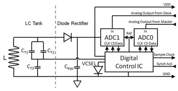
Block diagram of the back-end subunit showing the LC power receiver tank circuit, diode rectifier, SAR-ADCs, digital control IC, and VCSEL.
Fig. 7.

Microphotograph of the back-end subunit.
The two ADCs are successive-approximation ADCs (LTC2366) commercially available from Linear Technology Corporation [12]. The LTC2366 is a 12-bit ADC with a serial interface. It features low power dissipation and high speed and can operate up to 3MSps with a power dissipation of less than 7 mW at a supply voltage of 3 V. In order to achieve 12 effective bits, the ADC requires a minimum of 14 clock periods for a single conversion cycle that is initiated by an active “LOW” chip select signal (CS_N). The chip select signal is set LOW for 14 clock cycles and then HIGH for 10 clock cycles. The two chip select signals for the ADCs are then offset from one another by 12 clock cycles as shown in Figure 9.
Fig. 9.
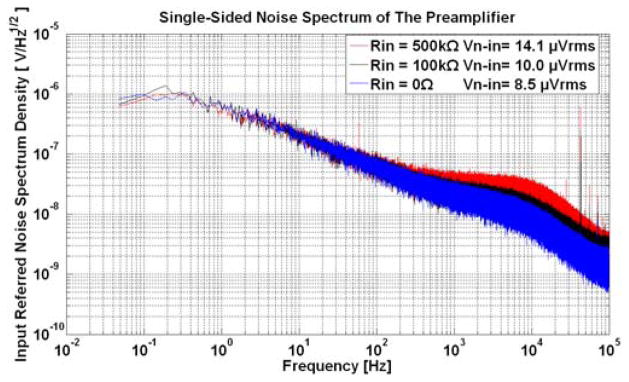
Input referred noise spectrum density of the preamplifier with different input resistances. The integration of these curves from 0.1Hz to 100 kHz yields an rms noise of 8.5μVrms, 10.0μVrms, and 14.1μVrms with input resistance of 0Ω, 100kΩ, 500kΩ respectively.
The digital control block is a custom design ASIC that requires six inputs including: VDD, GND, two ADC digital data signals, “synchronize acknowledge” from the master front-end, and the 500 mVpp power carrier. As mentioned above, the digital control ASIC uses the 500 mVpp power carrier to generate the main clock through an on-chip clock comparator. It produces the clock and chip select signals for the ADCs, as well as the sample clock for the dual front-end from that main clock. The two ADC chip select signals are also offset from each other by 12 main clock cycles. Therefore, the two ADCs are enabled alternatively. As a result, their data outputs are aligned in such a way that in a single sample clock period (24 cycles of main clock) the 12 effective bits of each ADC data are aligned back to back, leaving no redundant bits in the digital serial data stream. The rising edge of the “synchronize acknowledge” signal indicates the end of the last sample in a single frame (32 samples for the dual front-end system). On detecting this rising edge, the digital ASIC injects a 24-bit synch pattern into the serial digital data stream. This makes demultiplexing and data recovery at the receiving end possible.
A commercial 850 nm infrared VCSEL in an SMT 0603 package from Optowell Co. [13] is used as the transcutaneous wireless data transmitter. The digital control ASIC also incorporates an on-chip VCSEL driver that modulates the VCSEL current and thereby the VCSEL light intensity with the serial digital data stream. Once the modulated infrared light passes through the skin it is received by an external IR photosensor unit. This detector has a large-area silicon PIN diode coupled to a PMMA light-pipe that is brought into proximity with and aligned to the skin area right above the neurosensor implant. The light pipe, photosensor and RF source coil are mounted in a single small, light-weight coaxial package.
III. Fabrication
The fabrication of the system is divided in three sections: Section A focuses on integrating the front end amplifiers with the microelectrode array, Section B on backing and populating the flexible Kapton substrate and Section C on encapsulating the system using epoxy and polydimethylsiloxane (PDMS).
A. Integrating the front end amplifiers with the microelectrode array
Integrating the intracortical microelectrode arrays to the front-end amplifier ASIC presents a significant challenge due to restrictions imposed by the amplifier and array design. These are pressure and temperature constraints on the amplifier connections to the array and on the metal electrode contacts at the base of the array. The preamplifiers have double polysilicon input capacitors buried underneath the input pads, the electrode arrays have parylene insulation that has limited tolerance for high temperature, and the base of the array has only limited fracture strength. In addition, simultaneous bonding of all 16-channels was required. These constraints made assembly by soldering or ultrasonic bonding very difficult.
A modified flip-chip process strategy was developed using thermally cured, electrically conductive, Silver epoxy to avoid these issues. The two-part Silver epoxy (Epotek Model H20E-PFC) was prepared and inserted into a needle and syringe for use with a pneumatic dispenser. Previously, a pin stamping (epoxy dot) technique was employed but this method is slow and presented reliability issues due to the applied pressure on the input pads of the capacitors. A 32-gauge precision tip needle from Nordson EFD with an Ultra 2400 Series pneumatic dispenser from the same vendor allowed rapid and reliable dispensing of epoxy over the amplifier pads.
The 4 × 4 intracortical microelectrode arrays were purchased from Blackrock Microsystems with electrode heights of 1.5 mm. They were assembled into a specialized holder (GaAs housing) as previously described in [7] and flip chip bonded together using an RD Automation Model M9A unit. They were cured for 1hr at 90°C in the machine and then for 3hrs at 90°C on a hotplate in room air.
B. Backing and populating the flexible Kapton substrate
The flexible Kapton substrates were fabricated to our design specifications by MicroConnex Inc. They consisted of a dual layer flexible circuit with 18-25-18 Kapton, copper-ENEG metallization and had 27 μm Kapton cover coats on both sides (as well as small hole for the IR laser transmission). Sapphire backing plates (254 μm thick) were attached to the back-end and front-ends to provide a rigid support surface for supporting the device components and wire bonding without affecting the high flexibility provided by the tethering scheme. Sapphire was selected because it provides high mechanical strength as well as optical transparency to allow IR laser transmission through the device system. A 25 μm thick type JADE-A Rogers Film was used as the bonding agent. The sapphire was attached using a fast lamination process at ~300psi, 190°C for 1hr. After bonding, the film was mechanically removed from the VCSEL hole area at the center of the back-end to avoid interference with the optical data transmission.
The passive and active device components were populated on the back-end and front-ends of the substrate using the same Silver epoxy used for the flip-chip process and the epoxy was cured on a hotplate at 90°C. The controller and amplifier ASICs were wirebonded to the substrate using an ultrasonic wedge bonder with 1 mil Al-Si wire and finally two 5mil thick 90%Pt-10%Ir wires were attached with Silver epoxy to pads on the back-end. These wires are used as a common voltage reference electrode input to all the preamplifiers.
C. Encapsulating the system using epoxy and PDMS
Encapsulating the system for ensuring a good barrier for the implant to be isolated from body tissue (and vice versa) is the last step in completing the full fabrication process flow. This process secures all components and wirebonds using a Hysol epoxy (M-31 CL) followed by complete system encapsulation using PDMS (Nusil R-2188, [14]).
IV. Device Details and Characterization
The preamplifier ASICs and the digital control ASIC were fabricated in the AMI 0.5μm 2-poly 3-metal process through the MOSIS service on die that measure 2.2 mm × 2.2 mm and 2.0 mm × 2.0 mm respectively (Figs. 2 and 8). As already shown above in Fig. 1 (b), the two ASICs were integrated along with other components on an “L” shape flexible Kapton substrate with two tethers through the fabrication process described in Section III. The size of the neurosensor is 45.5 mm × 34.9 mm × 3 mm. The back-end connects to one end of each tether and measures 16.6 mm × 12.2 mm × 3 mm. Each front end is 5.4 mm × 4.5 mm × 3 mm, including the 1.5 mm long microelectrodes.
Fig. 2.

Microphotograph of the preamplifier ASIC fabricated in the AMI 0.5μm 2-poly 3-metal process through the MOSIS service
Fig. 8.

Microphotograph of the digital control ASIC fabricated in the AMI 0.5μm 2-poly 3-metal process through the MOSIS service.
The preamplifier has a measured bandwidth of 0.1 Hz to 7.8 kHz with an in-band gain of 45.6 dB (i.e. compatible with the demands of a broadband neural signal that includes spikes and LFPs). The input referred root-mean-square (rms) noise of the preamplifier alone is extracted from the output noise when the input is grounded. During this measurement the output noise is measured from the standard deviation of the output voltage sampled at 200 kSps over 20 seconds. An example of the input noise spectral density measurements is shown in Fig. 9. Integration from 0.1 Hz to 100 kHz yields an input referred noise of 8.5 μVrms. This value increases to 10.0 μVrms ~ 14.1 μVrms after including the thermal noise of the microelectrodes resistance with a typical range from 100 kΩ to 500 kΩ. The functionality of the digital control ASIC is validated by measuring the ADC control signals, sample clock, analog output signals, and the alignment of these signals. The waveforms of those signals match exactly to the design requirements discussed in Section II.
Finally, the entire neurosensor microsystem is tested wirelessly on the bench top using the setup shown in Fig. 10. The device is mounted on a station with three degrees of freedom and the external powering and receiving unit is positioned 10 mm below the neurosensor. A sharp metal probe is biased with a 1 KHz sine wave and brought 2 mm above the microelectrodes. This allows a weak sine wave signal (as a proxy to a neural signal) to be coupled to the microelectrodes through the air gap. The test is carried out in two parts, first with the probe over the master array and then with the probe over the slave array. The recorded waveforms from both experiments are shown in Fig. 11 (a) and (b) respectively. The display signals with odd channel numbers correspond to channels from the master front-end, and those with the even channel numbers correspond to channels from the slave front-end. The results shown in Fig. 11 clearly demonstrate the complete functionality of the dual-neurosensor. When the sine wave is applied to either of the front-ends (Master Fig. 11 (a) or Slave Fig. 11 (b)), the corresponding channels at the receiver show amplified sine waves on them. The entire system draws ~28mW at 3V supply voltage. The power dissipation of each block is shown in Table I.
Fig. 10.
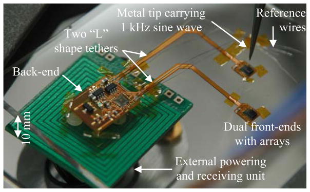
Bench-top measurement setup for testing the neurosensor.
Fig. 11.

Wirelessly recorded sine wave signals delivered to the neurosensor through the air gap on bench. (a) The sine wave is applied to the master front-end while leaving the inputs of the slave floating. (b) The sine wave is applied to the slave front-end while leaving the inputs of the master floating.
TABLE I.
Power Dissipation Distribution of The Entire Neurosensor
| Blocks | Power Dissipation |
|---|---|
| Master front-end | 1.4mW |
| Slave front-end | 1.4mW |
| Digital control ASIC | 10mW (9mW for the VCSEL driver) |
| Two SAR-ADCs | 9.6mW [12] |
| Diode rectifier | 2mW |
| LC tank | 3mW |
| Total | 28.4mW |
V. Conclusion
We have presented the implementation of a wireless, fully implantable microelectrode array-based neurosensor for intracortical recording from neural circuits at multiple locations. The detailed system architecture, circuit block diagram, fabrication and testing scheme for an initial device which can access two cortical sites were described. In the device version described above, transcutaneous digital telemetry is implemented by a microcrystal high-speed semiconductor laser. The neurosensor is currently being transitioned in a pig model for in vivo system validation. Further work at the device level of this scalable concept includes an increase to 10 × 10 intracortical MEAs for 100 channel broadband recording, expansion to three or more cortical areas and further integration of the very low power microelectronic components.
Acknowledgments
This work was supported in part by the National Institute of Health (NIBIB and NCMRR/NICHD, 1R01EB007401-01), and the National Science Foundation under the EFRI Program (#0937848).
References
- 1.Elston GN, Benavides-Piccione R, DeFelipe J. A study of pyramidal cell structure in the cingulate cortex of the macaque monkey with comparative notes on inferotemporal and primary visual cortex. Cerebral Cortex. 2005;15(1):64–73. doi: 10.1093/cercor/bhh109. [DOI] [PubMed] [Google Scholar]
- 2.Schneidman E, Berry M, Segev R, Bialek W. Weak pair-wise correlations imply strongly correlated network states in a neural population. Nature. 2006;440:1007–1012. doi: 10.1038/nature04701. [DOI] [PMC free article] [PubMed] [Google Scholar]
- 3.Pillow JW, Shlens J, Paninski L, Sher A, Litke AM, Chichilnisky EJ, Simoncelli EP. Spatio-temporal correlations and visual signaling in a complete neuronal population. Nature. 2008;454:995–999. doi: 10.1038/nature07140. [DOI] [PMC free article] [PubMed] [Google Scholar]
- 4.Turccolo W, Hochberg LR, Donoghue JP. Collective dynamics in human and monkey sensorimotor cortex: predicting single neuron spikes. Nature Neuroscience. 2010;13:105–111. doi: 10.1038/nn.2455. [DOI] [PMC free article] [PubMed] [Google Scholar]
- 5.Jones EG, Coulter JD, Hendry SH. Intracortical connectivity of architectonic fields in the somatic sensory, motor and parietal cortex of monkeys. J Comp Neurol. 1978;181:291–347. doi: 10.1002/cne.901810206. [DOI] [PubMed] [Google Scholar]
- 6.Blackrock Microsystems. Cereport multiport array. Available: http://www.blackrockmicro.com/en/micro-electrode-arrays-products.html#multiport.
- 7.Patterson WR, Song YK, Bull CW, Deangelis AP, Lay C, McKay JL, Nurmikko AV, Donoghue JP, Connors BW. A microelectrode/microelectronic hybrid device for brain implantable neuroprosthesic applications. IEEE Trans Biomed Eng. 2004 Oct;51(10):1845–1853. doi: 10.1109/TBME.2004.831521. [DOI] [PubMed] [Google Scholar]
- 8.Olsson RH, III, Gulari MN, Wise KD. A fully integrated bandpass amplifier for extracellular neural recording. Proc. 1st Int. IEEE-EMBS Conf. Neural Engineering; 165–168, Mar. 2003. [Google Scholar]
- 9.Harrison RR, Charles C. A low-power, low-noise CMOS amplifier for neural recording applications. IEEE J Solid-State Circuits. 2003 Jun;38(6):958–965. [Google Scholar]
- 10.Wattanapanitch W, Fee M, Sarpeshkar R. An energy-efficient micropower neural recording amplifier. IEEE Trans Biomed Circuits Syst. 2007 Jun;1(2):136–147. doi: 10.1109/TBCAS.2007.907868. [DOI] [PubMed] [Google Scholar]
- 11.Yin M, Ghovanloo M. A low-noise preamplifier with adjustable gain and bandwidth for biopotential recording applications. Proc. IEEE Intl. Symp. on Circuits and Systems; May 2007.pp. 321–324. [Google Scholar]
- 12.Linear Technology Corporation. LTC2366 - 3Msps, 12-Bit Serial ADCs in TSOT-23. http://www.linear.com/product/LTC2366.
- 13.Optowell Co. XS85-S0603-5U, single mode 850nm SMD VCSEL. http://www.optowell.com/bbs/board.php?board=vcselpackage&category=5.
- 14.NuSil Silicone Technology. R-2188, silicone elastomer. http://www.silicone-polymers.co.uk/pdf2007/R-2188P.pdf.
- 15.Patterson William R, III, Song YK, Bull C, Laiwalla F, Nurmikko Arto, Donoghue JP. CMOS ICs for Brain Implantable Neural Recording Microsystems. In: Westervelt R, Lee H, editors. Applications of CMOS circuits in Biology. Springer; 2007. pp. 259–292. [Google Scholar]