Abstract
Understanding how micro- and nanoparticles interact is important for achieving bottom-up assembly of desired structures. Here, we examine the self-assembly of two-component, compositionally asymmetric nanocylinders that sediment from solution onto a solid surface. These particles spontaneously formed smectic arrays. Within the rows of an array, nanocylinders tended to assemble such that neighboring particles had the same orientation of their segments. As a probe of interparticle interactions, we classified nanocylinder alignments by measuring the segment orientations of many sets of neighboring particles. Monte Carlo simulations incorporating an exact expression for the van der Waals (vdW) energy indicate that differences in the vdW interactions, even when small, are the key factor in producing observed segment alignment. These results point to asymmetrical vdW interactions as a potentially powerful means of controlling orientation in multicomponent cylinder arrays, and suggest that designing for these interactions could yield new ways to control self-assembly.
Keywords: Electrostatics, Self-Assembly, Monte Carlo, Nanowire, Nanotube, Computational, Hamaker
Understanding and exploiting interparticle interactions has long been a goal of the nano- and micro-particle assembly community. A traditional approach has been to take advantage of electrostatic or steric repulsions to prevent uncontrolled particle aggregation due to van der Waals (vdW) attractions.1–5 Combining these forces with chemical or biochemical recognition between surface molecules2–4,6 and/or additional physical forces such as entropic depletion,1,4 solvent evaporation,1–3 or the application of an external field2–4,6,7 has enabled well-controlled structures to be formed, most typically from uniform populations of single-component, spherical particles.
As the geometrical and compositional complexity of particles to be assembled increases, new challenges and opportunities for assembly present themselves. Single component rodlike particles typically assemble with their long axes parallel, often into smectic rows and in some cases in vertically oriented arrays that stand up on a substrate.8–17 If the two ends of the particles are different, they can be oriented within an array either pointing the same direction as their neighboring particles, pointing oppositely, or in a random mixture of orientations. Controlling particle orientation for anisotropic particles such as nanorods or nanowires is of interest to many researchers working to integrate these particles into devices such as sensors18–23 or energy storage24–32/collection33–38 materials. Multicomponent cylindrical particles with lengths of several microns and diameters on the order of hundreds of nanometers are readily prepared by template electrodeposition methods39,40 with segments of various metallic, semiconducting, and/or conducting polymer materials.41–45 Coatings can be added post-synthesis.9,10,44–49 These not only allow surface functionalization but also can provide the additional opportunity to etch away some segments leaving behind air- or solvent-filled gaps, with the structure maintained by the coating material.8,9,45–47,50–52 Hence, the materials properties of the segments along the length of these particles can be varied over a large range. While the fabrication of segmented multicomponent particles is relatively simple and has been the subject of extensive work,41,42,45 controlling their assembly orientation can be challenging and has been much less studied. A few examples have appeared in which the orientation of individual particles within a larger assembly has been controlled. Using electric fields, the Zheng group has aligned axially doped Si wires.53 Additionally, the Mirkin group has fabricated elaborate 3D structures from segmented Au and polypyrrole particles by a combination of hydrophobic, templating, and capillary effects.54–57 In both of these examples, orientational ordering was driven primarily by an external means, such as, the electric field or template, rather than by self-assembly of the particles due to intrinsic interparticle interactions.
Previously, our group has shown alignment of segmented particles in the vertical orientation. Partially-etched nanowires (PENs) composed of a silica shell that surrounds a core of Au segments and solvent-filled segments, sedimented from water to form arrays of particles consistently oriented with the Au end on the surface and the hollow (water-filled) silica end on the top.8,9 These assemblies were completed without solvent evaporation or the application of external fields, under the influence of gravity.8,9 The standing orientation was facilitated by the offset center-of-mass of the PENs, which had one dense end (Au-filled) and one less-dense end (solvent-filled). Particle diffusion was also important in this assembly strategy since it allowed PENs to convert to orientations that best optimize the vdW interactions of the Au cores.8,9
To fully understand the roles of vdW and electrostatic interactions it is necessary to combine experimental techniques with theoretical modeling. From a theoretical point of view, understanding the interactions between nanoparticles in solvent is still challenging. Molecular dynamics simulations have been used to understand the balance between vdW, electrostatic, and solvation (hydration) forces for atomically explicit models of nanoparticles in solvent.58–64 However, such detailed simulations cannot probe the length and time scales that are often associated with assembly. To this end, coarse-grained mesoscale models have been applied to understand nanoparticle assembly.10,65–68 For example, our group has worked previously on assemblies of solid Au nanowires (2–7 μm in length, 300 nm diameter).10 In that work, we were able to attribute the experimental observation of smectic rows to a balance of vdW and electrostatic interactions using Monte Carlo (MC) simulations in a coarse-grained model of the Au nanowires.10
Here, we explore interparticle interactions by examining nanocylinder orientation within smectic rows of segmented nanocylinders ca. 4 μm in length and 300 nm in diameter composed of Au, Ag, and/or hollow silica segments. Assemblies were completed in deionized water suspension without the presence of applied fields or solvent evaporation and were observed using optical microscopy. Quantitative measurements were combined with MC simulations to probe the affects of particle materials and segment sizes.
Results and Discussion
Figure 1 shows an assembly of silica-coated Au-Ag nanowires (300 nm diameter, 4 μm long particles with approximately 2 μm segments of Au and of Ag). Images were acquired 24 h after placing an aqueous suspension of the particles into a sealed chamber. Similarly to experiments with single segment Au nanowires,10 smectic rows of varying quality were observed in different regions across the sample. Ag and Au segments can be distinguished based on differences in their reflectivity;43,69,70 the Ag segments appear brighter. The region shown in Figure 1A is striking in that the nanowires are not only organized into smectic rows, but individual particles within each row are also oriented with their Ag ends facing in the same direction. This particular region contacted the air/water interface as the sample began to dry, which may have influenced assembly. This degree of striking orientational ordering was not typical. Other regions of the same sample, such as the one shown in Figure 1B, showed varying degrees of smectic order, and lacked the striking orientational ordering of Figure 1A. However, on close inspection smaller areas of orientational ordering could still be seen, as shown in the insets.
Figure 1.
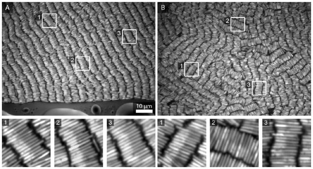
Reflectance optical microscope images showing different regions of the same sample of self-assembled Au-Ag nanowires in deionized water. (A) An exceptionally well-ordered region in which individual nanowires are oriented the same way within smectic rows. (B) Another region, more representative of the full assembly. For clarity, insets show enlarged views of the corresponding numbered regions within each of the top panels. Assemblies were formed on glass coverslips and all optical microscopy images were acquired from below.
The orientational ordering of Figure 1 was observed in the absence of applied fields, for particles with uniform silica coatings in the absence of binding interactions or templates. This was a surprising result because Au and Ag segments have similar materials properties. We therefore set out to determine what caused this orientational ordering, and whether it could be better controlled.
Determining Orientational Ordering
When qualitatively examining the arrays of Figure 1, the eye is drawn to regions where multiple nanowires are aligned. While not all of our images displayed such strong ordering, many images had regions indicating order. However, these regions do not necessarily indicate a non-random distribution of nanowire orientations within a full array. To allow comparison between samples, it is necessary to quantify orientational ordering.
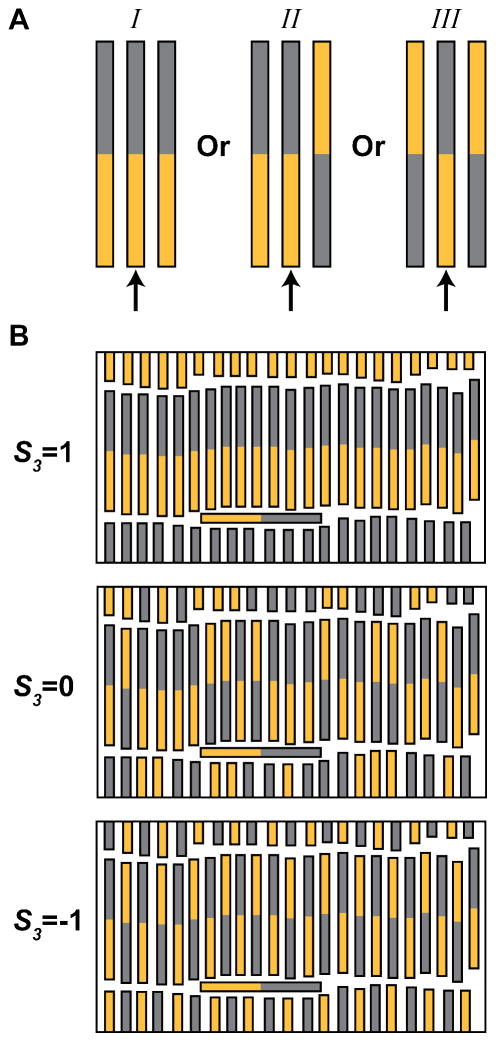
Here, we examined regions of well-aligned rows and focus on orientation within the rows. Well-aligned smectic regions of an assembly were defined and analyzed as described in the Methods section. Each nanowire can be oriented relative to its nearest neighbors in one of three ways, as illustrated in Figure 2A. Neighboring wires on the left and right could both face the same way as the central wire (↑↑↑, categorized as I), one could face the opposite direction (↑↑↓, ↓↑↑, categorized as II), or both could face the opposite direction (↓↑↓, categorized as III). Because there are two ways to achieve category II but only one way to achieve I or III, we can anticipate a ratio of 1: 2: 1 (I: II: III) for the random case where no orientation is energetically more favorable than another. Orientational ordering within an examined population is determined by tabulating these nearest neighbor interactions for each particle. We used a triplet order parameter: S3, which is defined as
Figure 2.
A) Possible ordering configurations for a particle and its two neighbors. With reference to the middle wire, the neighbors can be aligned the same way, partially aligned the same, or both oppositely aligned. B) The bottom three images show both of the extreme S3 values (1 and −1) and a random sample (S3 = 0). We note that calculations of S3 only consider the two immediately adjacent nanowires, not those within neighboring rows above and below.
| (1) |
To determine S3, cylinders with two nearest neighbors were classified into one of three categories defined in Figure 2A. The totals for the three categories (NI, NII, NIII) were then used to calculate the S3 value using Eq. 1. Figure 2B shows three potential observations and their resulting S3 values where 1 indicates all neighbors oriented the same direction, and −1 indicates alternating orientations. An S3 value of 0 indicates random orientations, with no tendency to have orientational order. We adopted this definition of S3 to quantify the type of ordering observed experimentally and in the simulations. Note that regions of apparent orientational ordering will still appear in random assemblies (Figure 2B) and that areas with the same S3 value may visually appear to have different order (Supporting Figure S1); this underscores the importance of quantification when interpreting images such as Figure 1. In Figure 1, frames A and B have S3 values of 0.57 and 0.13 for their well-ordered smectic regions, respectively. Supporting Table 1 contains analysis results from the images in Figure 1 and four additional images acquired during that experiment.
Overall orientational ordering for Au-Ag assemblies
We repeated the experiment from Figure 1, using a new batch of well-characterized nanowire populations and avoiding drying during assembly (see Table 1 for S3 analysis and Supporting Table 2 for particle characterization). Five separate assemblies of the same nanowire batch were prepared, each was imaged in ten or more randomly selected regions that showed good smectic rows. To calculate the S3 value, we examined at least 1000 nanowire sets from those five assemblies, as described in Methods. The average S3 value was 0.15 ± 0.07, with individual assemblies ranging from 0.09 to 0.25 (Table 1). The ratio of categories I: II: III was 1.9: 2.7: 1. These data indicate a slight preference for Au and Ag segments on adjacent nanowires to match orientations. The exceptionally good ordering of Figure 1A clearly represents an anomaly and ordering of that quality was not seen in any of the repeat samples, suggesting that unintended factors such as drying-related forces, sample contamination, and/or oxidation of the Ag segments may have been responsible for the higher orientational ordering in that region of that sample. These data underscore the importance of repeated experiments and quantification in interpreting assembly results. Additionally, though, the smaller S3 values observed on average in the Ag-Au samples appear to be nonrandom and suggest that some degree of orientational ordering is occurring.
Table 1.
Analysis of Au-Ag nanowire assemblies
| Sample | Number of Wires | S3 | |||
|---|---|---|---|---|---|
| ↑↑↑ | ↑↑↓ | ↑↓↑ | Total | ||
| 1 | 328 | 609 | 227 | 1164 | 0.09 |
| 2 | 606 | 764 | 214 | 1584 | 0.25 |
| 3 | 396 | 569 | 186 | 1151 | 0.18 |
| 4 | 327 | 502 | 210 | 1039 | 0.11 |
| 5 | 480 | 665 | 313 | 1458 | 0.11 |
| Total | 2137 | 3109 | 1150 | 6396 | 0.15 |
| Average | 0.15 ± 0.07 | ||||
What is the explanation for this small but reproducible orientational preference? In the absence of applied fields or chemical bonding, particle self-assembly is typically understood in terms of electrostatic repulsions and vdW attractive forces.1,4,5 The Au-Ag nanowires used in these experiments are coated in a thin, uniform layer of silica. The silica shells are negatively charged, and should provide constant electrostatic repulsions along the length of the particles that would not provide a driving force for orientational ordering. We also examined assemblies with a variety of other electrostatically repulsive coatings, including polyelectrolytes, 2-mercaptoethanesulfonic acid, and thiolated DNA oligonucleotides (Supporting Figure S2). Supporting Tables 3–5 summarize these results, all of which were quite similar to the silica-coated Ag-Au nanowires, with S3 values between 0.1 and 0.2. The similarity between S3 values for Au-Ag wire assemblies with a wide range of electrostatically-repulsive coatings (inorganic and organic, including single-point and multipoint attachment) indicates that the identity of the coating is unimportant for orientational ordering. It also argues strongly against any role for anisotropic electrostatic repulsion along the wire length that might be anticipated to arise from differences in coating on the different metals.
Since the nanowire cores contain segments of Au and Ag, small differences in their Hamaker constants (A), indicate a difference in their vdW attractions along the length of the wire. Both metals have relatively large and similar A values, with some disagreement as to the actual values depending on literature sources. 71,72 Could small differences in Hamaker constant between the Au and Ag segments drive the partial orientational ordering observed in Table 1? To address this question, we developed a computational model to explore these interactions for segmented nanowire assembly.
Model System
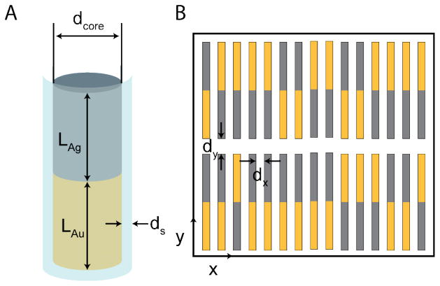
To understand the experimental ordering of the Au-Ag nanowires, we simulate the relative orientation of their Au and Ag segments using MC methods. We simulate core-shell nanowires, with a bimetallic Au-Ag core and a uniform silica shell. Figure 4A shows the essential elements of a simulated nanowire. We consider the nanowires to be segmented cylinders, with a total length of L = LAu + LAg + 2ds, where LAu and LAg are the lengths of the Au and Ag segments and ds is the shell thickness. The total nanowire diameter is d = dcore + 2ds, where dcore is the diameter of the metal core. Wires had a 2.4 μm segment of Au and a 2.3 μm segment of Ag. Nanowire diameters were 290 nm; and they had an amorphous silica coating 38 nm thick as determined by measurement of TEM images (Figure 3B and Supporting Table 2). Based on these numbers, we used LAu = LAg = 2.35 μm, ds = 38.0 nm, and dcore = 290 nm. Experimentally, the wires exhibit quasi-smectic ordering (cf., Figure 1), which we consider to be perfectly smectic for the purpose of our study. We also assume that the wires have uniform heights above the substrate, and exist in a single layer, so that they form a two-dimensional array. Experimental assemblies typically have sufficient particles to form between two to three monolayers, and hence are not two-dimensional, however we are only able to image the bottom layer.10
Figure 4.
A) Essential elements of a core-shell segmented Au-Ag nanowire, with an Au segment of length LAu, an Ag segment of length LAg, a silica shell of uniform thickness ds, and a metallic core diameter of dcore. B) A diagram of a smectic nanowire array in which only the metallic cores are shown. Au is gold and Ag is gray. Nanowires are separated by a spacing of dx along the rows and dy is the inter-row spacing.
Figure 3.
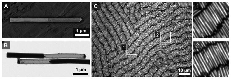
Images and assemblies of Au-Ag nanowires. Representative scanning (A) and transmission (B) electron microscopy images of these particles. Due to atomic number, in (A) the Au segments are brighter while the Ag segment is darker. This wire was imaged prior to silica coating in order to clearly show the Au and Ag segments; these can be obscured by the coating, which charges in the SEM. Due to electron density differences, in (B) the silica coating appears gray while the Au segments are black. The Ag segment has been etched for contrast and to enable TEM analysis of wire dimensions. C) Optical reflectance image of an assembly obtained after 24 hours. Two insets, denoted by white boxes in the main image, better show individual nanowires; Ag segments appear brighter due to their higher reflectivity. Assemblies were formed on glass coverslips and all optical microscopy images were acquired from below.
Figure 4B shows a snapshot of a portion of a simulated smectic nanowire array with randomly aligned Au and Ag segments (S3 ≈ 0). We adopt a wire spacing in the x direction perpendicular to the nanowire axes of dx = 200 nm and a y-spacing parallel to the nanowire axes of dy = 300 nm – these were experimentally estimated to be approximately 200 ± 50 nm and between 100 and 500 nm, respectively. (See Methods section for details regarding particle spacings.)
The total potential energy in our model system Etot is given by
| (2) |
where EvdW is the vdW energy, Ees is the electrostatic energy, and Eg is the gravitational energy. Since the nanowires in our model have uniform heights above the substrate, the gravitational force is constant and does not influence their relative alignment. Similarly, if the nanowires always remain in a perfectly smectic array and have a uniform silica coating, electrostatic interactions between the nanowires are constant and do not influence their relative orientation. Thus, vdW interactions are the key factor that affects the relative nanowire orientations. We note that at the nanowire separations relevant for this study, dispersion interactions are significantly retarded and likely negligible. At such long separations, the non-retarded, zero-frequency orientation and induction energies (which scale with distance as r−6) dominate the vdW interaction.5
To model core-shell vdW interactions between the cylindrical nanowires, we follow the derivations by Vold73,74 and Vincent74 for core-shell spheres. In our model, the elements of which are illustrated in Figure 5, the total vdW interaction energy between two core-shell cylinders i and j with metal cores of types C1 and C2 and shells S is given by
Figure 5.
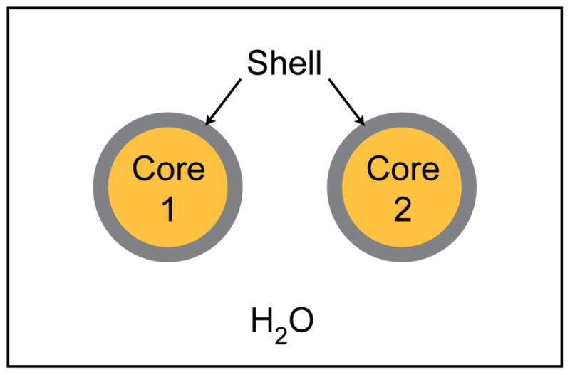
Cut-away view, looking down the nanowire axis, of two parallel core-shell nanowires with metal cores, silica shells, and water surrounding the wires.
| (3) |
where ES,S is the shell-shell interaction, EC1,S and EC2,S are the interactions between cores 1 and 2 and the shell, respectively, and EC1,C2 is the interaction between core 1 and core 2. The terms in Eq. (3) take the form
| (4) |
| (5) |
| (6) |
And
| (7) |
where AS, AW, AC1, and AC2 are the Hamaker constants for the shell, water, metal core 1, and metal core 2, respectively.
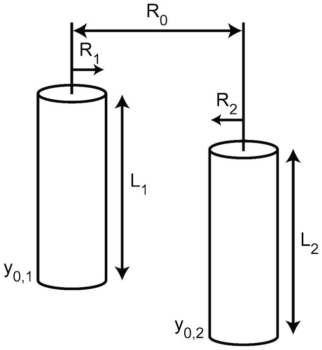
Figure 6 illustrates the essential elements of the H functions in Eqs. (4)–(7). For two cylinders with parallel axes, as would occur in a smectic nanowire array, the H functions have the form
Figure 6.
Illustration of the essential parameters for calculating the H function between two parallel cylinders using Eq. (8). y0,1 and y0,2 are the positions of the nanowire bases in our chosen coordinate system (cf., Figure 4B), R1 and R2 are the radii, L1 and L2 are the lengths of nanowire 1 and nanowire 2, respectively, and R0 is the distance between the two centers.
| (8) |
where
| (9) |
In Figure 6, we see that R0 is the distance between cylindrical axes along the x direction in our chosen coordinate system, and r, y, and θ are the radial, axial, and angular coordinates describing the wire geometry [cf., Figure 4B].
In general, Eq. (8) for H cannot be solved analytically – although analytical approximations to Eq. (8) exist for two, parallel, equal-length cylinders of length L with their ends aligned.77,78 In this case, we have
| (10) |
for R0–R1–R2 ≪ R1, R2 and
| (11) |
for R0 > R1, R2. In the limit of very large nanowire separations R0 ≫ R1, R2, the wires behave as point particles and their interaction is given by
| (12) |
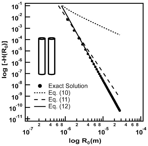
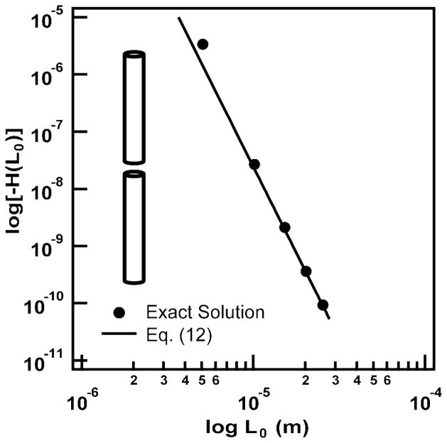
Figure 7 shows a logarithmic plot of Eqs. (10) – (12), along with the exact numerical solution of Eq. (8), which we obtained using Mathematica®. In this figure, we considered two parallel nanowire segments, each of length L = LAu and R1 = R2 = dcore/2, at separation intervals of nΔR0, where ΔR0 = dcore + 2ds + dx and n = {1, …, 49}. These correspond to the possible separations we would find along a nanowire row in the experimental nanowire arrays. In Figure 7, we see that the nanowire pair interaction energy decreases by approximately 10 orders of magnitude over a 27 μm distance. Equation (12) captures the exact solution at the longest nanowire separations, Eq. (11) comes close to the exact solution at short nanowire separations, and Eq. (10) comes close only at the shortest separation.
Figure 7.
Plot of Eq. (8) (exact solution), along with the approximate solutions of Eqs. (10)–(12) for two aligned, parallel cylinders, as shown in the inset.
To provide an idea of the relative nanowire interactions in this system, we also plot the exact solution of Eq. (8), along with the long-range solution given by Eq. (12) for two coaxial nanowire segments, each of length L = LAu and R1 = R2 = dcore/2, in Figure 8. The separation intervals between the wires in this figure are nΔL0, where ΔL0 = LAu + LAg+ 2ds + dy and n = {1, …, 5}. These correspond to the possible separations we would find between two coaxial nanowire segments in different smectic rows in the experiments. To compare the analytical and exact solutions, we replace R0 by L0 in Eq. (12). In Figure 8 we see that the inter-row interaction between nanowires is weak compared to the intra-row interaction and it decays rapidly across the rows. The inter-row interaction essentially matches the solution from Eq. (12) for all but the shortest nanowire separation.
Figure 8.
Plot of Eq. (8) (exact solution) along with the approximate solution of Eq. (12) for two co-axial cylinders, as shown in the inset.
To obtain the total energy in a smectic nanowire array with a given orientation of the wires, we add the pair interactions between various nanowire segments. For the core-core interactions, this sum has the form
| (13) |
where the sums run over all unique i-j nanowire pairs, over segments k and l in nanowires i and j, respectively, and ECk,Cl is given by Eq. (7). Similar to the electrostatic and gravitational forces, the vdW shell-shell and core-shell interactions are constant and do not depend on the relative nanowire orientations. Thus, Eq. (13) provides an effective expression for changes in the total energy of the system as we change the relative nanowire orientations.
To perform the MC simulations, we use a smectic nanowire array with 100 nanowires in the x direction [cf., Figure 4B] and 12 nanowires along the y direction, for a total of 1200 nanowires. We use periodic boundary conditions, so that the longest distances between nanowire pairs are the longest distances in Figures 7 and 8. In these figures, we also see that the interaction energy at the longest nanowire separations in the x and y directions is about 10 orders of magnitude smaller than that at the shortest separations. Thus, the dimensions of our simulation box are sufficient to eliminate finite-size effects.
In the MC simulations, a trial move consists of randomly choosing a nanowire and attempting to flip its orientation, by exchanging the positions of its Au and Ag segments. We note that this does not mimic the complex mechanisms (described below in the final section) by which nanowires change their orientations in the experimental system. The MC simulations are designed to predict equilibrium configurations of the smectic array and, as such, they do not consider kinetic phenomena. We use the Metropolis MC algorithm to accept the move with a probability given by
| (14) |
where ΔE = EvdW,f − EvdW,i is the difference between the total energies of the system in the final (f) and initial (i) states. The total energy is given by Eq. (13), which requires us to numerically evaluate the integral in Eq. (8) for all pairs of nanowire segments. Since multiple evaluations of this integral throughout the course of a MC simulation would considerably reduce the computational efficiency, we calculate the nanowire core-core interaction for all possible core-core pairs prior to commencing the MC simulations. We, then obtain this interaction from a look-up table when it is required in the simulation. Equation (13) also requires us to have Hamaker constants for Au, Ag, and silica – although a detailed analysis of Eqs. (7) and (13) indicates that the relative vdW energies of various nanowire configurations only depend on the relative Hamaker constants of Ag and Au and not on the shell material. We use values of AAu = 44.0 × 10⁻²⁰ J71 and Asilica = 7.0 × 10⁻²⁰ J. 72 The Hamaker constant for Ag AAg takes on values in the literature that vary between 20–45 × 10−20 J. 72 We examine the effect of varying AAg in this range.
The MC simulations were run at a temperature of 300 K. For each set of conditions, we ran 3 separate trials beginning with one perfectly ordered (S3 = 1) and two random initial conditions. Each run consisted of 200 attempted moves per site, or Monte Carlo steps (MCS) of equilibration, followed by 1000 MCS of production. The total energy fluctuated about a constant value at the end of the equilibration stage and remained in this range throughout the production runs. We obtained the value of S3 using Eq. (1) as an average of values measured every MCS.
Simulation Results For Ag-Au Nanowires
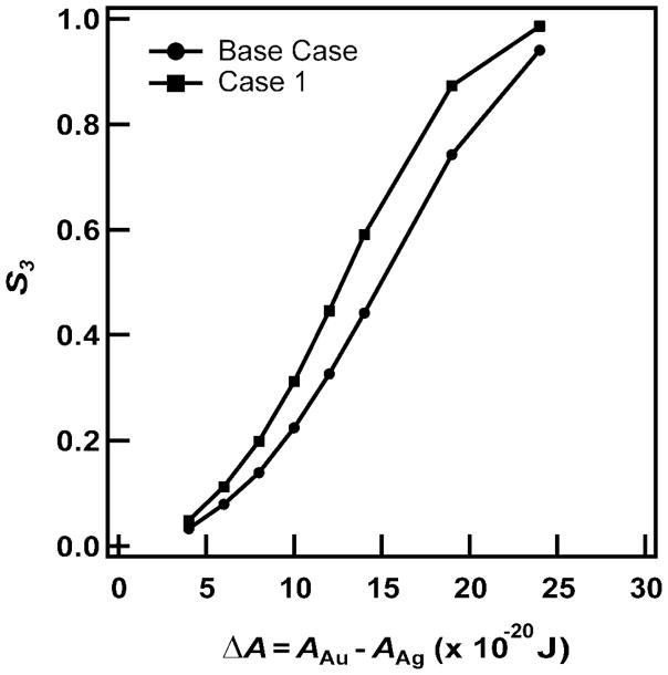
Figure 9 shows S3 as a function of the difference ΔA between the Hamaker constants of Au and Ag for AAg ranging from 20 to 40 × 10−20 J. Here, we see that S3 increases as ΔA increases. This occurs because there is a greater energetic driving force for aligning Au segments as the difference between the Hamaker constants of Au and Ag increases. If Au and Ag had equal Hamaker constants (ΔA = 0), we would have S3 = 0, or no preferred ordering of the nanowires. The experimentally observed ordering for the base case (or the most likely experimental parameters, as discussed above) is consistent with ΔA ≈ 8 × 10⁻²⁰ J, or AAu = 44 × 10−20 J and AAg = 36 × 10−20 J. Also plotted in Figure 9 is another scenario (Case 1) in which dx = 180 nm and dcore = 310 nm were used and ΔA is observed to shift to the left so that the experimentally observed S3 would indicate AAg = 37.5 × 10⁻²⁰ J. Although these Hamaker constants fall well within the range of literature values, we emphasize that the calculations can only determine a value ΔA that is consistent with the experiments. The calculations cannot uniquely determine values of the Hamaker constants.
Figure 9.
S3 as a function of ΔA for the base case (most likely experimental parameters characterizing the nanowire arrays, as discussed in the text) and for Case 1, in which dcore = 310 nm and dx = 180 nm (cf., Figure 4).
Figure 10 shows selected snapshots for the base case. For ΔA = 24 × 10−20 J, S3 = 0.94 [Figure 10A] and we see long runs of aligned nanowires within the rows. At ordering consistent with the experimental conditions [Figure 10B] S3 = 0.14, the length of the aligned nanowire runs within the rows has decreased considerably. For ΔA = 4 × 10⁻²⁰ J, S3 = 0.033 [Figure 10C]. Such a value of S3 is easily achievable when we randomly generate initial nanowire alignments.
Figure 10.
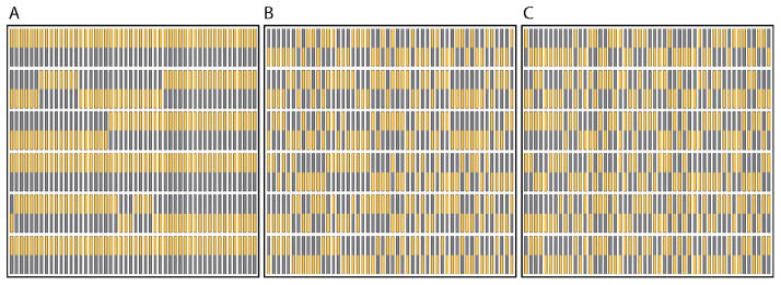
Snapshots of ¼ of the simulated lattice with the base-case nanowire array parameters for (a) ΔA = 24 × 10−20 J (S3 = 0.94); (b) ΔA = 8 × 10⁻²⁰ J (S3 = 0.14) and; (c) ΔA = 4 × 10⁻²⁰ J (S3 = 0.033). Au segments are shown in gold and Ag segments are shown in gray – the shell is not shown.
In addition to ΔA, the nanowire diameter and spacing – especially the spacing between nanowires in the same row – can influence nanowire alignment. Figure 9 shows results from simulations in which we used dcore = 310 nm, which is 20 nm thicker than the base-case value of 290 nm, and dx = 180, which is 20 nm smaller than the base value of 200 nm. We have selected these values as they fall within the observed range of nanowire diameters (± 50 nm) and interparticle spacings which are measured with optical microscopy and based on the nanowire diameter. (See Methods section for details regarding particle spacings and Supporting Table 2 for particle dimensions.) Here, we see that by increasing these values, we increase the value of S3 for a fixed ΔA. By increasing either dcore or dx, we increase the value of the integral in Eq. (8) and we, thus, endow a greater preference for energetically favored Au-Au side-by-side segments.
To understand the driving force for nanowire ordering, we defined the energy gain Egain for a pair of anti-parallel (anti) wires to assume a parallel (par) configuration as Egain = Eanti - Epar. Supporting Figure S3 shows Egain/kT as a function of nanowire separation for the first 10 neighbors within a nanowire row, assuming the base case parameters for the nanowire array. Here, we see that the energy gained by the nanowires in assuming a parallel interaction falls off dramatically with nanowire distance within a row. Indeed, the second-neighbor interaction is only about 2% of the nearest-neighbor value. We also see that Egain depends on the difference between the Au and Ag Hamaker constants. For the ΔAAg = 24.0 × 10⁻²⁰ J, where we find S3 ≈ 1, we see that Egain = 3.3kT per nearest-neighbor nanowire pair at 300 K. For a Hamaker constant of ΔAAg = 8.0 × 10⁻²⁰ J, which provides the best match between simulation and experiment for the base-case nanowire array parameters, we see that Egain = 0.28kT per nearest-neighbor nanowire pair at 300 K. Thus, a relatively small parallel energy gain can impart a significant degree of orientational ordering to the nanowires.
One way to experimentally increase ΔA is through the use of different segment materials. The templated synthesis method has been used to produce wires with a wide variety of segment materials from metals to polymers to molecular layers.41–43,45 Metals generally have the largest A values, while polymers, and amorphous materials and liquids are much smaller. Partially etched nanowires (PENs) are hybrid silica nanotube/nanowires that feature a glass shell around a partially metal-filled, partially solvent-filled core. These PENs assemble into either horizontal or vertical arrays based on their segment properties.8,9 Based on our previous studies, we concluded that a PEN designed with a 2 μm segment of Au, a 1 μm etched segment, and a terminal 1 μm Au segment should create smectic arrays (as opposed to the vertically oriented arrays often seen).8,9 Within the rows, PENs have a larger difference in vdW interactions based on their orientation compared to the all metallic Au-Ag wires of above.
PEN Simulations
To simulate the assembly of these particles we used the three segment PENs with dimensions defined in Figure 11. Following the experimental measurements (Supporting Table 2), we used L2Au = 2.4 μm, LAu = LE = 1.3 μm, and dcore = 270 nm. ds, dx, and dy assumed the values we used for the Au-Ag nanowires. For three-segment PENs the total vdW interaction between core segments is given by
Figure 11.
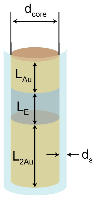
Schematic of a PEN, characterized by two Au segments, one of length L2Au and one of length LAu, and an empty, solvent-filled segment, of length LE. The shell thickness is ds and the core diameter is dcore.
| (15) |
where the sums run over the three segments. To evaluate ECk,Cl, we use Eqs. (7) and (8), taking the Hamaker constant for water to be AW = 3.73 × 10⁻²⁰ J.5 Since the Hamaker constant for the solvent-filled segment is considerably less than those of either Ag or Au, there is a strong preference for the PENs to align their long Au segments. Thus, in simulations of PEN arrays characterized by the experimental parameters, we predict S3 = 0.99 at 300 K.
A snapshot from our simulation is shown in Figure 12. Here, we see that not only are the long (and short) Au segments aligned along rows, but there is also inter-row ordering that favors the pairing of long Au segments with other long Au segments and as a result short Au segments pair with other short ones.
Figure 12.
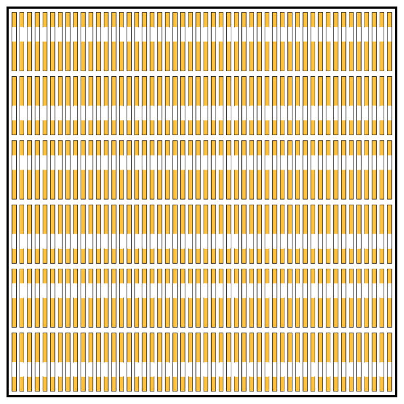
Snapshot of ¼ of the simulated lattice for PENs. Au segments are gold and solvent-filled segments are white.
Assembly of PENs
We synthesized PENs matching the dimensions given above with the simulations; characterization data for these particles can be found in Supporting Table 2. Figure 13 shows a SEM and TEM image of the type of particle and an image of the assembly using optical reflectance microscopy. As expected, the assemblies formed horizontal, smectic rows. Here, the etched segments are much less reflective than the Au and hence generally appears as black as the background.8,9 The etched segment, which can be seen in the TEM image, can be distinguished by the spacing of the two Au segments in the optical micrograph, since inter-row spacings are much smaller.10 Figure 14 shows additional images from these assemblies showing the differences in S3 across a single sample. Despite some variation across the sample (Frame A S3 = 0.29, Frame B S3 = 0.40), orientational ordering in these samples is typically higher than for the Au-Ag wires.
Figure 13.
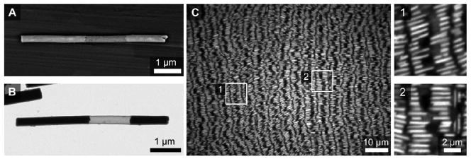
Images and assemblies of PENs. Representative scanning (A) and transmission (B) electron microscopy images of these wires. C) Optical reflectance image of an assembly obtained after 24 hours had elapsed. Two insets, denoted by white boxes in the main image, better show individual PENs. The wire in frame A was imaged prior to silica coating and etching to show the presence of the Ag segment. Once coated, the segments can be obscured by charging on the silica in the SEM. Frame B shows the actual particles used for assembly where the Au segments are black and the silica shell is gray. In the optical micrographs, the etched segments appear dark due to their low reflectivity and partial transparency. Assemblies were formed on glass coverslips and all optical microscopy images were acquired from below.
Figure 14.
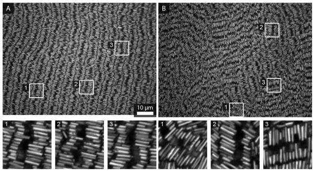
Optical reflectance images showing various areas across a single assembly of PENs. White boxes highlight regions that are expanded in the insets below. Assemblies were formed on glass coverslips and all optical microscopy images were acquired from below.
Experimentally Determined S3 Values for PEN Assemblies
We determined the average S3 value from five separate assemblies of PENs to be 0.33 ± 0.09 (Table 2). This value is over twice as high as we observed for the Au-Ag wires, and a single assembly (≥10 images, ≥1000 PENs) gave an average S3 value as high as 0.47. This average S3 value, driven solely by vdW differences, approaches that of the anomalous region of Figure 1A, which probably formed due to drying effects. Thus, designing the particles to maximize vdW differences along their length did greatly improve orientational ordering in the experiments.
Table 2.
Analysis of Au-cored PENs
| Sample | Number of Wires | S3 | |||
|---|---|---|---|---|---|
| ↑↑↑ | ↑↑↓ | ↑↓↑ | Total | ||
| 1 | 780 | 663 | 182 | 1625 | 0.37 |
| 2 | 713 | 483 | 105 | 1301 | 0.47 |
| 3 | 491 | 460 | 144 | 1095 | 0.32 |
| 4 | 404 | 468 | 147 | 1019 | 0.25 |
| 5 | 611 | 699 | 221 | 1531 | 0.25 |
| Total | 2999 | 2773 | 799 | 6571 | 0.33 |
| Average | 0.33 ± 0.09 | ||||
Although S3 values for PENs were much higher than for Au-Ag wires, they were significantly lower than the perfect orientational ordering predicted by the model. This can be understood in terms of differences between the experiment and model. Real assemblies may be unable to reach true thermodynamic minima and instead be trapped in metastable states. For example, individual particles cannot actually flip to sample orientational energies in the experiments. Rather, they exchange with particles in an upper layer that may already have a more preferred orientation.10 The presence of particle multilayers, while providing a mechanism for increasing S3 by swapping out misoriented particles, also inhibits the movement of any individual particle and as such can depress S3 values. Additionally, improved orientational ordering within an assembly works against this exchange mechanism, since the odds of having a wire with opposite orientation in the upper layer are higher when the energetic cost of misorientation is low. We believe this contributed to the lower-than-predicted experimental S3 values in our PEN assemblies. Because the etched regions of the PENs are transparent, it is in fact possible to see that differently oriented wires in the upper layer are relatively rare in these assemblies (Supporting Figure S4).
Two other key differences between the experiment and model should be noted: (1) The particle population is reasonably monodisperse, but also includes defect wires (branched, bundled, or broken particles). These interfere with the overall assembly. (2) Although the model is limited to a perfect smectic array, the experiment can sample other arrangements that can reduce the energetic cost of misorientation. For example, particles within a row can be offset, and/or can interdigitate with adjacent rows (Figure 15 and Supporting Figure S5). Figure 15 shows an example of “misoriented” PENs that have shifted their position within the row to optimize attractive interactions between Au segments on adjacent particles. Such observations suggest that it should be possible to further improve orientational ordering by enforcing smectic rows, ensuring fully 2-D assemblies without any multilayers, and/or improving particle monodispersity.
Figure 15.
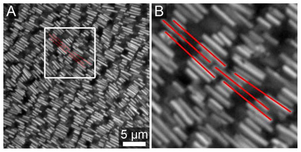
Reflectance optical images of a PEN assembly that illustrates one way particles may offset to gain more favorable interactions. Frame A shows a region of PENs in loosely smectic rows. Frame B shows an enlargement of the area highlighted by the white box, and outlines (red) six PENs from neighboring smectic rows. The middle PENs are shifted so that the long end of the lower PEN fills space left open by the short end of the top PEN between two longer Au segments. By increasing the interactions between the gold ends this essentially aligns the etched segments of these PENs, reducing the cost of “misorientation”.
Conclusions
Thus, we observed and documented the self-assembly of compositionally anisotropic nanocylinders. Inherent differences in the attractive vdW forces between different material segments in the cylinder led to orientational ordering. Through both experiments and MC simulations based on exact evaluation of the vdW interaction between the nanocylinders, we demonstrated that even a very small difference between the Hamaker constants of the different material segments can result in non-random alignment of the cylinders relative to their nearest neighbors within the overall assembly. We anticipate that the effects of anisotropic vdW forces between different regions of multicomponent particles will be observed more often as experimenters assemble increasingly complex particles. This could aid or hinder desired assembly orientations, depending on particle compositions and desired assembly outcomes, and should be considered. It is hoped that future research can design for, and take advantage of, these effects to better control orientational ordering in arrays of functional multicomponent particles, as a means of ultimately optimizing optical and electronic device performance.
Methods
Materials
All water used in these experiments was purified to >18.2 MΩ·cm, using a Barnstead Nanopure filtration system or was BDH Aristar Plus HPLC grade water (low TOC, VWR). Chemicals were used as received.
Nanowire Preparation
Nanowires were prepared via templated electrodeposition into porous alumina templates (nominal pore diameter 0.2 μm, Whatman) as described elsewhere.8,39,40,44,45 A gold cap (~100 nm) was included after the Ag segment of the Au-Ag nanowires to prevent it from etching during the dissolution of the working electrode layer (this cap was ignored in simulations). Amorphous silica coating followed previously published reports.8,9,46 Final PEN concentrations were determined using a Hausser Scientific Neubauer Hemacytometer.
Sample Preparation
Nanowires, 6 μL of 1.5 × 10⁹ nanowire/mL suspension, were pipetted into an assembly chamber comprised of a silicone spacer (CoverWell, Electron Microscopy Sciences) sealed to a glass cover slip. The spacer was 2.0 mm in diameter and 2.0 mm deep, creating a surface area of 0.031 cm2 for assembly and a total volume of 6.3 μL. For a 4 μm nanowire, this amount should produce between two and three monolayers of horizontally aligned particles. Before addition to the chamber, the nanowire suspension was sonicated to randomly distribute nanowires throughout the suspension and reduce particle aggregation. The chambers were placed on the microscope stage before the nanowires were added. Once the wires were added to the chamber, it was sealed completely with another cover slip to prevent evaporation. These cover slips were left on the microscope for 24 hours before imaging; all imaging was completed before 25.5 h had elapsed.
Imaging
Imaging was performed on a Nikon TE200 inverted microscope using reflected white light from a Hg bulb and 100× oil (NA 1.4) objective. Approximately 30 images were obtained per sample and eight samples from the same nanowire synthesis batch were imaged sequentially. No observed aggregation or stickiness, for example, to the substrate, in the sample was allowed, and areas with a minimum of broken, bundled, or clumped particles were imaged. Nanowire segments were identified by differences in the reflectivities of the metals.38,65,66 Although contrast between Au and Ag can be maximized by using only short-wavelength illumination and/or filtering the reflected light, here we used the entire spectrum of the Hg bulb so that both Au and Ag segments could be clearly distinguished from the non-reflective background; this provided sufficient contrast between Au and Ag segments to distinguish them.
Image Analysis
The orientational ordering within arrays of nanowires was compared for nanowires in well-ordered sections of the images, hereafter referred to as rectangles. Each rectangle contained a minimum of seven nanowires all of the same length (± 20 %), none of which were visibly branched. All of the nanowires within a rectangle were fully in the plane of focus, directly next to the adjacent nanowire within that row, and shifted by no more than 20% of the nanowire length (up or down) from the adjacent nanowires. Only rectangles within 30 degrees of the axis perpendicular to the space between the rows were counted (i.e., the wires generally formed a parallelogram with corner angles not less than 60 degrees). Selection of “well-ordered sections” is illustrated in Supporting Figure S6. Examples of rectangles used in determination of S3 values and those omitted from use in calculating S3 values are illustrated in Supporting Figure S7. Within a rectangle, the nanowires were analyzed in sets of three wires focusing on the middle nanowire. Counts placed wires in one of three categories: all nanowires in the same direction (↑↑↑); one adjoining nanowire the same direction with the other in the opposite direction (↑↑↓); or all nanowires alternating (↓↑↓). A minimum of 1000 nanowires was counted for each experiment and the totals for five experiments were averaged. We note that no trend in S3 values with row length was observed (Supporting Figure S8).
Particles spacings were determined by averaging measurements and Fourier transform analysis. Intrarow spacings (i.e., the spacing between the short axes of nanowires within a row) were determined by measuring a series of ten wires. Measurements were taken for ten spots across five images in each sample. Subtraction of the average wire width (determined by measurement of TEM images) gave a measure of the spacing, approximately 200 ± 50. These values matched those previously observed for similar assemblies.10,77 Interrow spacings (i.e., the spacing between the long axes of nanowires) has been previously determined by Fourier transform analysis.10, 77 Those sources show that the spacing of multiple assemblies varies between 100 and 500 nm, which match the assemblies seen herein.
Supplementary Material
Acknowledgments
Experimental aspects of this research were primarily supported by the Donors of the American Chemical Society Petroleum Research Fund (ACS PRF 50888-ND10). Transmission electron microscope images were collected at the Penn State Microscopy and Cytometry Facility - University Park, PA and scanning electron microscope images were collected using the Materials Characterization Lab at Penn State. Preliminary computational studies were partially funded by the National Science Foundation IGERT DGE-9987589 (D. A. T.) and the computational work presented here was supported the US Department of Energy, Office of Basic Energy Sciences, Materials Science Division, grant number DE-FG02-07ER46414 (K. A. F.). Initial experimental observations of possible ordering in MESA-coated Au-Ag wires were made while performing work funded by the National Institutes of Health (R01 EB000268). Undergraduates D. H. R. and P. G. were supported by NSF grants DMR 0648837 and DMR 0820404.
Footnotes
Online supporting information includes additional tables of nanocylinder dimensions and S3 values of nanowires with non-silica coatings. Images are provided to further describe the determination of S3. Methods for and supporting figures of non-silica coatings are included. This material is available free of charge via the Internet at http://pubs.acs.org.
References and Notes
- 1.Min Y, Akbulut M, Kristiansen K, Golan Y, Israelachvili J. The Role of Interparticle and External Forces in Nanoparticle Assembly. Nat Mater. 2008;7:527–538. doi: 10.1038/nmat2206. [DOI] [PubMed] [Google Scholar]
- 2.Li F, Josephson DP, Stein A. Colloidal Assembly: The Road From Particles to Colloidal Molecules and Crystals. Angew Chem Int Ed USA. 2011;50:360–388. doi: 10.1002/anie.201001451. [DOI] [PubMed] [Google Scholar]
- 3.Kinge S, Crego-Calama M, Reinhoudt DN. Self-Assembling Nanoparticles at Surfaces and Interfaces. Chem Phys Chem. 2008;9:20–42. doi: 10.1002/cphc.200700475. [DOI] [PubMed] [Google Scholar]
- 4.Bishop KJM, Wilmer CE, Soh S, Grzybowski BA. Nanoscale Forces and Their Uses in Self-Assembly. Small. 2009;5:1600–1630. doi: 10.1002/smll.200900358. [DOI] [PubMed] [Google Scholar]
- 5.Israelachvili JN. Intermolecular and Surface Forces. 3. Academic Press; Burlington, MA: 2011. [Google Scholar]
- 6.Grzelczak M, Vermant J, Furst EM, Liz-Marzán LM. Directed Self-Assembly of Nanoparticles. ACS Nano. 2010;7:3591–3605. doi: 10.1021/nn100869j. [DOI] [PubMed] [Google Scholar]
- 7.Smith BD, Mayer TS, Keating CD. Deterministic Assembly of Functional Nanostructures Using Nonuniform Electric Fields. Annu Rev Phys Chem. 2012;63:241–263. doi: 10.1146/annurev-physchem-032210-103346. [DOI] [PubMed] [Google Scholar]
- 8.Smith BD, Kirby DJ, Keating CD. Vertical Arrays of Anisotropic Particles by Gravity-Driven Self-Assembly. Small. 2011;7:781–787. doi: 10.1002/smll.201002233. [DOI] [PubMed] [Google Scholar]
- 9.Smith BD, Kirby DJ, Ortiz Rivera I, Keating CD. Self-Assembly of Segmented Anisotropic Particles: Tuning Compositional Anisotropy to Form Vertical or Horizontal Arrays. ACS Nano. 2013;7:825–833. doi: 10.1021/nn305394s. [DOI] [PubMed] [Google Scholar]
- 10.Triplett DA, Quimby LM, Smith BD, Rodríguez DH, St Angelo SK, González P, Keating CD, Fichthorn KA. Assembly of Gold Nanowires by Sedimentation from Suspension: Experiments and Simulation. J Phys Chem C. 2010;114:7346–7355. doi: 10.1021/jp909251v. [DOI] [PMC free article] [PubMed] [Google Scholar]
- 11.Baker JL, Widmer-Cooper A, Toney MF, Geissler PL, Alivisatos AP. Device-Scale Perpendicular Alignment of Colloidal Nanorods. Nano Lett. 2010;10:195–201. doi: 10.1021/nl903187v. [DOI] [PubMed] [Google Scholar]
- 12.Singh A, English NJ, Ryan KM. Highly Ordered Nanorod Assemblies Extending Over Device Scale Areas and in Controlled Multilayers by Electrophoretic Deposition. J Phys Chem B. 2013;117:1608–1615. doi: 10.1021/jp305184n. [DOI] [PubMed] [Google Scholar]
- 13.Dogic Z, Fraden S. Smectic Phase in a Colloidal Suspension of Semiflexible Virus Particles. Phys Rev Lett. 1997;78:2417–2420. [Google Scholar]
- 14.Purdy KR, Fraden S. Influence of Charge and Flexibility on Smectic Phase Formation in Filamentous Virus Suspensions. Phys Rev E. 2007;76:011705. doi: 10.1103/PhysRevE.76.011705. [DOI] [PubMed] [Google Scholar]
- 15.Tao AR, Huang J, Yang P. Langmuir–Blodgettry of Nanocrystals and Nanowires. Acc Chem Res. 2008;41:1662–1673. doi: 10.1021/ar8000525. [DOI] [PubMed] [Google Scholar]
- 16.Sau TK, Murphy CJ. Self-Assembly Patterns Formed upon Solvent Evaporation of Aqueous Cetyltrimethylammonium Bromide-Coated Gold Nanoparticles of Various Shapes. Langmuir. 2005;21:2923–2929. doi: 10.1021/la047488s. [DOI] [PubMed] [Google Scholar]
- 17.Gu Z, Chen Y, Gracias DH. Surface Tension Driven Self-Assembly of Bundles and Networks of 200 nm Diameter Rods Using a Polymerizable Adhesive. Langmuir. 2004;20:11308–11311. doi: 10.1021/la047937o. [DOI] [PubMed] [Google Scholar]
- 18.Sioss JA, Bhiladvala R, Pan W, Li M, Patrick S, Xin P, Dean SL, Keating CD, Mayer TS, Clawson GA. Nanoresonator Chip-Based RNA Sensor Strategy for Detection of Circulating Tumor Cells: Response Using DD3 As a Prostate Cancer Marker. Nanomedicine. 2011;8:1017–1025. doi: 10.1016/j.nano.2011.11.009. [DOI] [PMC free article] [PubMed] [Google Scholar]
- 19.Patolsky F, Lieber CM. Nanowire Nanosensors. Mater Today. 2005;8:20–28. [Google Scholar]
- 20.Chen X, Wong CKY, Yuan CA, Zhang G. Nanowire-Based Gas Sensors. Sensor Actuat B – Chem. 2013;177:178–195. [Google Scholar]
- 21.Penner RM. Chemical Sensing with Nanowires. Annu Rev Anal Chem. 2012;5:461–485. doi: 10.1146/annurev-anchem-062011-143007. [DOI] [PubMed] [Google Scholar]
- 22.Patolsky F, Zheng G, Lieber CM. Nanowire Sensors for Medicine and the Life Sciences. Nanomedicine. 2006;1:51–65. doi: 10.2217/17435889.1.1.51. [DOI] [PubMed] [Google Scholar]
- 23.Morrow TJ, Li M, Kim J, Mayer TS, Keating CD. Programmed Assembly of DNA-Coated Nanowire Devices. Science. 2009;323:352. doi: 10.1126/science.1165921. [DOI] [PMC free article] [PubMed] [Google Scholar]
- 24.Gowda SR, Reddy ALM, Zhan X, Jafry HR, Ajayan PM. 3D Nanoporous Nanowire Current Collectors for Thin Film Microbateries. Nano Lett. 2012;12:1198–1202. doi: 10.1021/nl2034464. [DOI] [PubMed] [Google Scholar]
- 25.Vlad A, Reddy ALM, Ajayan A, Singh N, Gohy JF, Melinte S, Ajayan PM. Roll Up Nanowire Battery From Silicon Chips. Proc Natl Acad Sci USA. 2012;109:15168–15173. doi: 10.1073/pnas.1208638109. [DOI] [PMC free article] [PubMed] [Google Scholar]
- 26.Qiu MC, Yang LW, Qi X, Li J, Zhong JX. Fabrication of Ordered NiO Coated Si Nanowire Array Films As Electrodes for a High Performance Lithium Ion Battery. ACS Appl Mater Interfaces. 2010;2:3614–3618. doi: 10.1021/am100791z. [DOI] [PubMed] [Google Scholar]
- 27.Chan CK, Peng H, Liu G, McIlwrath K, Zhang XF, Huggins RA, Cui Y. High-Performance Lithium Battery Anodes Using Silicon Nanowires. Nat Nanotechnol. 2008;3:31–35. doi: 10.1038/nnano.2007.411. [DOI] [PubMed] [Google Scholar]
- 28.Gowda SR, Reddy ALM, Zhan X, Ajayan PM. Building Energy Storage Device On a Single Nanowire. Nano Lett. 2011;11:3329–3333. doi: 10.1021/nl2017042. [DOI] [PubMed] [Google Scholar]
- 29.Shaijumon MM, Ou FS, Ci L, Ajayan PM. Synthesis of Hybrid Nanowire Arrays and Their Application As High Power Supercapacitor Electrodes. Chem Commun. 2008:2373–2375. doi: 10.1039/b800866c. [DOI] [PubMed] [Google Scholar]
- 30.Astromskas G, Storm K, Karlström O, Caroff P, Borgström M, Wernersson LE. Doping Incorporation in InAs Nanowires Characterized by Capacitance Measurements. J Appl Phys. 2010;108:054306. [Google Scholar]
- 31.Astromskas G, Storm K, Wernersson LE. Transient Studies on InAs/HfO2 Nanowire Capacitors. Appl Phys Lett. 2011;98:013501. [Google Scholar]
- 32.Liu R, Duay J, Lee SB. Heterogeneous Nanostructured Electrode Materials for Electrochemical Energy Storage. Chem Commun. 2011;47:1384–1404. doi: 10.1039/c0cc03158e. [DOI] [PubMed] [Google Scholar]
- 33.Spurgeon JM, Atwater HA, Lewis NS. A Comparison Between the Behavior of Nanorod Array and Planar Cd(Se, Te) Photoelectrodes. J Phys Chem C. 2008;112:6186–6193. [Google Scholar]
- 34.Garnett EC, Brongersma ML, Cui Y, McGehee MD. Nanowire Solar Cells. Annu Rev Mater Res. 2011;41:269–295. [Google Scholar]
- 35.Kelzenberg MD, Boettcher SW, Petykiewicz JA, Turner-Evans DB, Putnam MC, Warren EL, Spurgeon JM, Briggs RM, Lewis NS, Atwater HA. Enhanced Absorption and Carrier Collection in Si Wire Arrays for Photovoltaic Applications. Nat Mater. 2010;9:239–244. doi: 10.1038/nmat2635. [DOI] [PubMed] [Google Scholar]
- 36.Garnett EC, Yang P. Silicon Nanowire Radial p-n Junction Solar Cells. J Am Chem Soc. 2008;130:9224–9225. doi: 10.1021/ja8032907. [DOI] [PubMed] [Google Scholar]
- 37.Garnett E, Yang P. Light Trapping in Silicon Nanowire Solar Cells. Nano Lett. 2010;10:1082–1087. doi: 10.1021/nl100161z. [DOI] [PubMed] [Google Scholar]
- 38.Wallentin J, Anttu N, Asoli D, Huffman M, Aberg I, Magnusson MH, Siefer G, Fuss-Kailuweit P, Dimroth F, Witzigmann B, et al. InP Nanowire Array Solar Cells Achieving 13. 8% Efficiency by Exceeding the Ray Optics Limit. Science. 2013;339:1057–1060. doi: 10.1126/science.1230969. [DOI] [PubMed] [Google Scholar]
- 39.Al-Mawlawi D, Liu CZ, Moskovits M. Nanowires Formed in Anodic Oxide Nanotemplates. J Mater Res. 1994;9:1014–1018. [Google Scholar]
- 40.Hulteen JC, Martin CR. A General Template-Based Method for the Preparation of Nanomaterials. J Mater Chem. 1997;7:1075–1087. [Google Scholar]
- 41.Kline TR, Tian M, Wang J, Sen A, Chan MWH, Mallouk TE. Template-Grown Metal Nanowires. Inorg Chem. 2006;45:7555–7565. doi: 10.1021/ic0601384. [DOI] [PubMed] [Google Scholar]
- 42.Wang J. Template Electrodeposition of Catalytic Nanomotors. Faraday Discuss. 2013 doi: 10.1039/c3fd00105a. [DOI] [PubMed] [Google Scholar]
- 43.Nicewarner-Peña SR, Freeman GP, Reiss BD, He L, Peña DJ, Walton ID, Cromer R, Keating CD, Natan NJ. Submicrometer Metallic Barcodes. Science. 2001;294:137–141. doi: 10.1126/science.294.5540.137. [DOI] [PubMed] [Google Scholar]
- 44.Keating CD, Natan MJ. Striped Metal Nanowires As Building Blocks and Optical Tags. Adv Mater. 2003;15:451–454. [Google Scholar]
- 45.Hurst SJ, Payne EK, Qin L, Mirkin CA. Multisegmented One-Dimensional Nanorods Prepared by Hard-Template Synthetic Methods. Angew Chem Int Ed. 2006;45:2672–2692. doi: 10.1002/anie.200504025. [DOI] [PubMed] [Google Scholar]
- 46.Sioss JA, Keating CD. Batch Preparation of Linear Au and Ag Nanoparticle Chains via Wet Chemistry. Nano Lett. 2005;5:1779–1783. doi: 10.1021/nl051370u. [DOI] [PubMed] [Google Scholar]
- 47.Dean SL, Stapleton JJ, Keating CD. Organically Modified Silicas on Metal Nanowires. Langmuir. 2010;26:14681–14870. doi: 10.1021/la102070c. [DOI] [PMC free article] [PubMed] [Google Scholar]
- 48.Stoermer RL, Cederquist KB, McFarland SK, Sha MY, Penn SG, Keating CD. Coupling Molecular Beacons to Barcoded Metal Nanowires for Multiplexed, Sealed Chamber DNA Bioassays. J Am Chem Soc. 2006;128:16892–16903. doi: 10.1021/ja0658261. [DOI] [PMC free article] [PubMed] [Google Scholar]
- 49.Sha MY, Yamanaka M, Walton ID, Norton SM, Stoermer RL, Keating CD, Natan MJ, Penn SG. Encoded Metal Nanoparticle-Based Molecular Beacons for Multiplexed Detection of DNA. NanoBiotechnology. 2005;1:327–335. doi: 10.1385/NBT:1:4:327. [DOI] [PMC free article] [PubMed] [Google Scholar]
- 50.Qin L, Park S, Huang L, Mirkin CA. On-Wire Lithography. Science. 2005;309:113–115. doi: 10.1126/science.1112666. [DOI] [PubMed] [Google Scholar]
- 51.Banholzer MJ, Qin L, Millstone JE, Osberg KD, Mirkin CA. On-Wire Lithography: Synthesis, Encoding and Biological Applications. Nat Protoc. 2009;4:838–848. doi: 10.1038/nprot.2009.52. [DOI] [PMC free article] [PubMed] [Google Scholar]
- 52.Braunschweig AB, Schmucker AL, Wei WD, Mirkin CA. Nanostructures Enabled by On-Wire Lithography (OWL) Chem Phys Lett. 2010;486:89–98. doi: 10.1016/j.cplett.2010.01.009. [DOI] [PMC free article] [PubMed] [Google Scholar]
- 53.Lee CH, Kim DR, Zheng X. Orientation-Controlled Alignment of Axially Modulated pn Silicon Nanowires. Nano Lett. 2010;10:5116–5122. doi: 10.1021/nl103630c. [DOI] [PubMed] [Google Scholar]
- 54.Ciszek JW, Huang L, Wang Y, Mirkin CA. Kinetically Controlled, Shape Directed Assembly of Nanorods. Small. 2008;4:206–210. doi: 10.1002/smll.200700840. [DOI] [PubMed] [Google Scholar]
- 55.Park S, Lim JH, Chung SW, Mirkin CA. Self-Assembly of Mesoscopic Metal-Polymer Amphiphiles. Science. 2004;303:348–351. doi: 10.1126/science.1093276. [DOI] [PubMed] [Google Scholar]
- 56.Lim JK, Ciszek JW, Huo F, Jang JW, Hwang S, Mirkin CA. Actuation of Self-Assembled Two-Component Rodlike Nanostructures. Nano Lett. 2008;8:4441–4445. doi: 10.1021/nl802381h. [DOI] [PubMed] [Google Scholar]
- 57.Ciszek JW, Huang L, Tsonchev S, Wang Y, Shull KR, Ratner MA, Schatz GC, Mirkin CA. Assembly of Nanorods into Designer Superstructures: The Role of Templating, Capillary Forces, Adhesion, and Polymer Hydration. ACS Nano. 2010;4:259–266. doi: 10.1021/nn901383d. [DOI] [PubMed] [Google Scholar]
- 58.Qin Y, Fichthorn KA. A Molecular-Dynamics Simulation Study of Forces Between Colloidal Nanoparticles in a Lennard-Jones Liquid. J Chem Phys. 2003;119:9745–9754. doi: 10.1063/1.2776259. [DOI] [PubMed] [Google Scholar]
- 59.Qin Y, Fichthorn KA. Solvation Forces Between Colloidal Nanoparticles: Directed Alignment. Phys Rev E. 2006;73:020401. doi: 10.1103/PhysRevE.73.020401. [DOI] [PubMed] [Google Scholar]
- 60.Fichthorn KA, Qin Y. Molecular Dynamics Simulation of Colloidal Nanoparticle Forces. Ind Eng Chem Res. 2006;45:5477–5481. [Google Scholar]
- 61.Qin Y, Fichthorn KA. Molecular Dynamics Simulation of the Forces Between Colloidal Nanoparticles in n-Decane Solvent. J Chem Phys. 2007;127:144911. doi: 10.1063/1.2776259. [DOI] [PubMed] [Google Scholar]
- 62.Alimohammadi M, Fichthorn KA. Molecular Dynamics Simulation of the Aggregation of Titanium Dioxide Nanocrystals: Preferential Alignment. Nano Lett. 2009;9:4198–4203. doi: 10.1021/nl9024215. [DOI] [PubMed] [Google Scholar]
- 63.Dzubiella J, Hansen JP. Competition of Hydrophobic and Coulombic Interactions Between Nanosized Solutes. J Chem Phys. 2004;121:5514–5530. doi: 10.1063/1.1783274. [DOI] [PubMed] [Google Scholar]
- 64.Lane JMD, Ismail AE, Chandross M, Lorenz CD, Grest GS. Forces Between Functionalized Silica Nanoparticles in Solution. Phys Rev E. 2009;79:050501. doi: 10.1103/PhysRevE.79.050501. [DOI] [PubMed] [Google Scholar]
- 65.Zhang ZL, Glotzer SC. Self-Assembly of Patchy Particles. Nano Lett. 2004;4:1407–1413. doi: 10.1021/nl0493500. [DOI] [PubMed] [Google Scholar]
- 66.Damasceno PF, Engel M, Glotzer SC. Predictive Self-Assembly of Polyhedra into Complex Structures. Science. 2012;337:453–457. doi: 10.1126/science.1220869. [DOI] [PubMed] [Google Scholar]
- 67.Agarwal U, Escobedo FA. Mesophase Behaviour of Polyhedral Particles. Nat Mater. 2011;10:230–235. doi: 10.1038/nmat2959. [DOI] [PubMed] [Google Scholar]
- 68.Lukatsky DB, Mulder BM, Frenkel D. Designing Ordered DNA-Linked Nanoparticle Assemblies. J Phys Cond Matt. 2006;18:S567–S580. [Google Scholar]
- 69.Nicewarner-Peña SR, Carado AJ, Shale KE, Keating CD. Barcoded Metal Nanowires: Optical Reflectivity and Patterned Fluorescence. J Phys Chem B. 2003;107:7360–7367. [Google Scholar]
- 70.Walton ID, Norton SM, Balasingham A, He L, Oviso DF, Jr, Gupta D, Raju PA, Natan MJ, Freeman RG. Particles for Multiplexed Analysis in Solution: Detection and Identification of Striped Metallic Particles Using Optical Microscopy. Anal Chem. 2002;74:2240–2247. doi: 10.1021/ac020073w. [DOI] [PubMed] [Google Scholar]
- 71.Klimchitskaya GL, Mohideen U, Mostepanenko VM. Casimir and van der Waals Forces Between Two Plates or a Sphere (Lens) Above a Plate Made of Real Metals. Phys Rev B. 2000;61:062107. [Google Scholar]
- 72.Eichenlaub S, Chan C, Beaudoin SP. Hamaker Constants in Integrated Circuit Metallization. J Colloid Interface Sci. 2002;248:389–397. doi: 10.1006/jcis.2002.8241. [DOI] [PubMed] [Google Scholar]
- 73.Vold MJ. The Effect of Adsorption on the van der Waals Interaction of Spherical Colloidal Particles. J Colloid Sci. 1961;16:1–12. [Google Scholar]
- 74.Vincent B. The van der Waals Attraction Between Colloid Particles Having Adsorbed Layers. II. Calculation of Interaction Curves. J Colloid Interface Sci. 1973;42:270–285. [Google Scholar]
- 75.Langbein D. Van der Waals Attraction Between Cylinders, Rods, or Fibers. Phys Kondens Materie. 1972;15:61–86. [Google Scholar]
- 76.Parsegian VA. van der Waals Forces. Cambridge University Press; Cambridge UK: 2006. [Google Scholar]
- 77.Dillenback LM. PhD Dissertation. The Pennsylvania State University; University Park, PA: 2008. Self-Assembly and Controlled Assembly of Nanoparticles. [Google Scholar]
Associated Data
This section collects any data citations, data availability statements, or supplementary materials included in this article.


