Abstract
For intermediate-band solar cells, the broad absorption spectrum of quantum dots (QDs) offers a favorable conversion efficiency, and photocurrent generation via efficient two-step two-photon-absorption (TS-TPA) in QDs is essential for realizing high-performance solar cells. In the last decade, many works were dedicated to improve the TS-TPA efficiency by modifying the QD itself, however, the obtained results are far from the requirements for practical applications. To reveal the mechanisms behind the low TS-TPA efficiency in QDs, we report here on two- and three-beam photocurrent measurements of InAs quantum structures embedded in AlGaAs. Comparison of two- and three-beam photocurrent spectra obtained by subbandgap excitation reveals that the QD TS-TPA efficiency is improved significantly by suppressing the relaxation of hot TS-TPA carriers to unoccupied shallow InAs quantum structure states.
Obtaining a large enhancement in the efficiencies of converting solar energy to electrical energy is a challenging task. Many novel solar-cell operation principles have been proposed1,2,3,4,5,6, but for the realization of efficient energy conversion, a thorough understanding of the carrier dynamics in solar cells is a fundamental prerequisite. One operation principle is based on the energy conversion of low-energy photons: in the intermediate-band (IB) solar cell5, the energy of multiple low-energy photons is combined in the IB to create one high-energy electron–hole (e–h) pair. With the efficient conversion of IR photons to e–h pairs, it is possible to significantly exceed the Shockley–Queisser limit of single junction solar cells7.
The most-studied quantum structures for IBs are formed by InAs embedded in GaAs bulk, and prepared via self-assembly: a few-monolayer-thick disk-like and a few-nanometer-thick pyramidal quantum structures, referred to as quantum well islands (QWIs) and quantum dots (QDs) hereafter8,9 (see Methods for details). Due to the InAs QD growth mechanism, it is extremely difficult to prepare QD layers without any QWIs. It is for this reason that the photoluminescence (PL) and photocurrent (PC) excitation spectra reported by various researchers show an upconversion site well above the QD state (often referred to as a state in the rough wetting layer)10,11,12,13,14,15; the upconversion site is attributed to QWIs16,17.
QDs have been investigated intensively since their proposed application in IBs18, and their broad absorption spectrum has been considered to be advantageous for IBs. A prerequisite for realizing the predicted high efficiency of the IB solar cell5 is that the PC is generated effectively via two-step two-photon-absorption (TS-TPA)19 in the deep confined states of the QDs. However, experimentally observed weak TS-TPA transitions from QD confined states to continuum states have been interpreted as an inherently small TS-TPA absorption cross section of the QDs22,23,24. It has been suggested that without a suitable design, QD IBs cannot be used for practical devices20,21,25,26.
It is usually assumed that the hot carriers created by TS-TPA in QDs can easily escape to the barrier conduction band, and in such a case any modification should be made to the QD state itself for improvement. Several approaches to improve the TS-TPA upconversion efficiency from QDs have been proposed27,28,29. Some improvement in performance has been confirmed through these efforts, but the specific role of TS-TPA enhancement in QDs is still under discussion14,15,30,31,32. The overall low TS-TPA efficiency that has been observed experimentally in InAs QDs is a longstanding issue in IB solar cell research. To realize highly efficient IBs formed by QDs, the reason for the low TS-TPA efficiency must be identified.
In the present work, we have studied TS-TPA processes and their efficiencies in InAs QWIs and QDs using two- and three-beam excitation spectroscopy with tunable light sources. The crucial influence of the QWI occupation on the carrier escape mechanisms in the TS-TPA processes is identified for the first time. By suppressing the capture of TS-TPA carriers in QWIs, TS-TPA efficiencies of QDs can be improved significantly.
Results
Single- and two-beam experiments
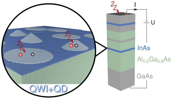
The sample structure used in this work is shown in Fig. 1 (see Methods for details). Growing InAs on GaAs or AlGaAs with MBE leads to the formation of pyramidal QDs and flat disk-like QWIs. Because the InAs quantum structures have different heights, the QWI states are situated at high energies, whereas the QD states are found at low energies. The PC is generated upon wavelength selective excitation of different structures and extracted via an applied bias. PC data at room temperature are shown in Figs. 2a,b. Figure 2a shows the PC intensity I(λB1) for single-beam excitation with a variable wavelength λB1 in red and PC intensity I(λB1, λIR) for two-beam excitation with a variable λB1 and fixed λIR = 1550 nm in blue obtained with excitation powers of PB1 = 8 mW and PIR = 1.5 mW, corresponding to excitation power densities of approximately 8 and 1.5 W/cm2, respectively. Details of the optical setup are given in the Methods, Measurement system section. Peaks in the PC spectra were assigned to carrier generation in the QWIs and QDs16. Single-beam experiments on QWIs16 and QDs33 have revealed that the major upconversion mechanisms are Auger34 and thermal processes, respectively.
Figure 1. Sample structure.
GaAs, AlGaAs, and InAs are shown in gray, green, and blue, respectively. Electrons and holes are shown as red and black spheres, respectively. The epitaxially grown sample structure on the right is connected electrically to obtain the PC (I) by subbandgap photon illumination (red arrow) and the applied bias (U). The magnified region shows the InAs/AlGaAs layer, which consists of disk-like QWIs and pyramidal QDs on top of a 1-ML wetting layer. Carriers are created by the absorption of subbandgap photons in the QWIs and QDs. After upconversion via the Auger or TS-TPA process, the carriers are extracted as current. The InAs/GaAs layer consists only of QWIs. A GaAs/AlGaAs QW was introduced for reference purposes.
Figure 2. TS-TPA contribution at 300 K and 30 K.
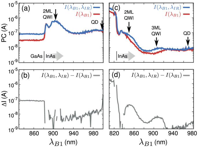
The PC due to single wavelength excitation (red) and that for additional excitation inducing intraband (confined to continuum) transitions (blue) are shown; the difference is shown in gray. The wavelength regime for the InAs excitation is indicated by the gray arrow. (a) Comparison of and (b) difference between the single- (I(λB1)) and two-beam (I(λB1, λIR)) PC spectra at 300 K. (c) Comparison of and (d) difference between the single- and two-beam PC spectra at 30 K. Characteristic features correspond to quantum structures (QDs and 2 and 3 monolayer (ML) thick QWIs). Here, PIR = 1.5 mW (about 1.5 W/cm2), and PB1 = 8 mW (about 8 W/cm2). λIR was fixed at 1550 nm.
By using a two-beam configuration with sufficiently high excitation power, the TS-TPA contribution can be revealed. In the present experimental setup we require more than about 1 W/cm2 average excitation power ( ) to obtain clear TS-TPA signals from all quantum structures. The difference between the two- and single-beam room-temperature data (Fig. 2b) gives a measure of the TS-TPA efficiency, since λIR = 1550-nm photons cannot create new carriers but only excite carriers above the barrier. No significant TS-TPA contribution from λIR = 1550-nm photons is observed in the InAs region at room temperature, and a contribution is observed at temperatures below 100 K, as shown in Figs. 2c and d. Note that the shape of the single wavelength data (red curve) in Fig. 2c has been discussed in our previous work16. On additional excitation with λIR, we see that the PC increases at several energy levels. We assigned, in accordance with the PL spectra, the peaks in Fig. 2d to PC generation via TS-TPA processes in GaAs (λ < 820 nm), 2-ML-thick QWIs (λ ≈ 850 nm), 3-ML-thick QWIs (λ ≈ 900 nm), and QDs (λ > 960 nm). Because shallow QWIs have the highest PC generation efficiency, from this point, “QWI” is used to refer only to QWIs with emission and absorption at about 850 nm. The TS-TPA signatures arise for excitation of well-defined quantum structures, which are formed for a wide range of growth conditions. A quantitative analysis of this TS-TPA contribution is required.
Detailed temperature dependence
Figure 3 shows the temperature dependence of the PC generated by the excitation of QWIs and QDs. At each temperature, λB1 was tuned to the QWI and QD energy levels. The measured total PC I(λB1) (large dots) consists of contributions from TS-TPA processes in both quantum structures as well Auger processes in the QWIs16 and thermal upconversion in the QDs33. To estimate the TS-TPA contribution, the PC I(λB1, λIR) for excitation with beam 1 (B1) and an additional IR beam was measured. The PC difference between the two- and single-beam excitation, I(λB1, λIR) − I(λB1), is the TS-TPA contribution due to IR excitation. This TS-TPA contribution was evaluated at each temperature, and subtracted from the total measured PC (large dots), resulting in an evaluated PC without TS-TPA contribution (small dots). The differences between the broken and solid curves visualize the contribution of TS-TPA to the PC (colored area). The figure shows qualitatively that the TS-TPA processes in both QWIs and QDs are much weaker than the Auger process observed in QWIs. The PC due to TS-TPA is only observed at low temperatures, and TS-TPA has no significant contribution to PC at room temperature. We note that at low temperatures, the TS-TPA efficiency for QD excitation is about an order weaker than for QWI excitation.
Figure 3. TS-TPA temperature dependence of PC contribution for QWI and QD excitation.
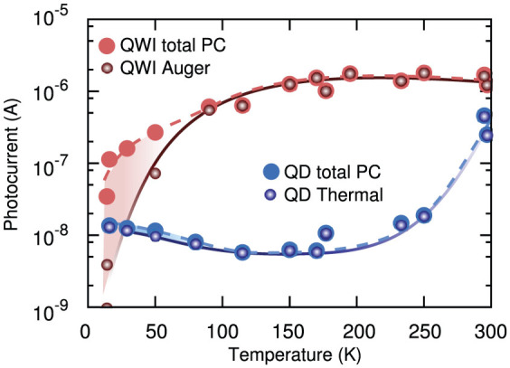
PC intensities obtained for excitation at the 2 ML QWI state energy (red) and at the high energy edge of the QD states (blue). The total PC, including the TS-TPA contribution is shown by the large dots (the dashed curve is a guide for the eye). The PC due to the major upconversion mechanisms (Auger process for QWIs and thermal process for QDs), i.e., without the TS-TPA contribution, is shown by the small dots (the solid curve is a guide for the eye). A significant TS-TPA contribution is observed below 100 K, as shown by the difference between the dashed and solid curves (shaded region).
Two- and three-beam maps
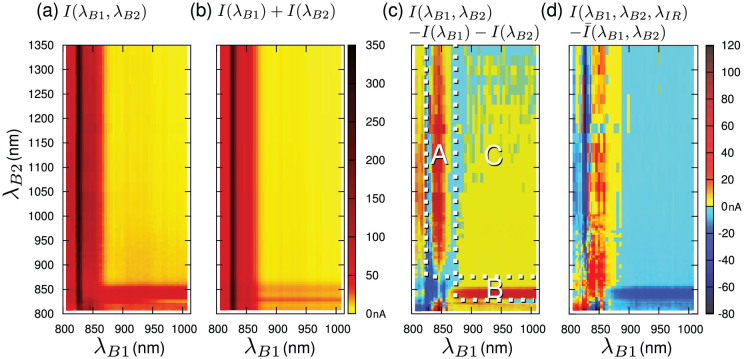
Two- and three beam experiments were carried out to clarify the limiting factor of PC generation via TS-TPA in QDs using the experimental setup, shown in Fig. 4. Total and evaluated PC contributions obtained from single-, two-, and three-beam experiments are compared in Fig. 5. The maps are plotted as functions of the excitation wavelengths λB1 and λB2, and the two-beam map is obtained by scanning both λB1 and λB2 from short to long wavelengths. The PC intensity map I(λB1, λB2) in Fig. 5a is for simultaneous excitation with both beams, while Fig. 5b shows the sum I(λB1) + I(λB2) of two PC wavelength scans, measured by single excitations with λB1 and λB2. The latter single-beam PC map does not contain effects due to simultaneous two-beam excitation. The difference between these two PC maps is the two beam effect, shown in Fig. 5c.
Figure 4. Experimental setup.
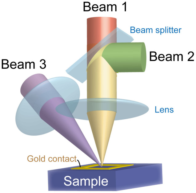
Beam 1 (λB1) and beam 2 (λB2) were aligned coaxially using a wedge beam splitter. The third beam (λIR) was aligned separately.
Figure 5. Two- and three-beam PC maps at 30 K.
Positive PC contributions are shown as yellow to red; negative PC contributions are shown as blue shades. (a) Total PC measured by simultaneous excitation using excitation sources B1 and B2 that results in the two-beam map I(λB1, λB2). Calculated PC contributions: (b) single-beam map I(λB1) + I(λB2), obtained by the sum of two single wavelength scans; (c) two-beam effect calculated by I(λB1, λB2) − I(λB1) − I(λB2), i.e., the difference between the PC maps in (b) and (a) (the regions A,B and C indicated with broken lines are discussed in the text); and (d) additional PC contribution due to a third beam that induces TS-TPA transitions only. This TS-TPA effect is calculated from  . Here, PB1 = 1 mW (about 1 W/cm2), PB2 = 140 μW (about 0.14 W/cm2), and PIR = 1.5 mW (about 1.5 W/cm2). λIR was fixed at 1550 nm.
Further, the TS-TPA effect due to an additional IR beam at 1550 nm is plotted in Fig. 5d. Note that the term “TS-TPA effect” is used to refer to the additional PC induced by means of TS-TPA transitions (no new carriers are created). The TS-TPA effect can be negative when carriers that have already been created in the QDs are excited to trap states, which is a process that does not contribute to the PC. A strong positive TS-TPA effect obviously means a high TS-TPA efficiency. The TS-TPA effect is calculated by subtracting the PC contribution of two-beams  from the three-beam PC data I(λB1, λB2, λIR) (if the two-beam effect is written as B1 ∩ B2 − B1 − B2 and the IR effect Bx ∩ IR − Bx we obtain by substitution the definition of
  ). This data will be discussed later. There are many features in the PC maps that deserve attention; however, we focus here on those features that have a bearing on the TS-TPA in the QDs.
The regions A and B in Fig. 5c correspond to excitation conditions in which one beam resonantly excites the shallow QWI states (λQWI = 850 – 880 nm, obtained from PL), and the second beam excites the lower lying states, e. g., QDs. In contrast, region C defines the case in which both beams excite the lower lying states, i.e., shallow QWI states are not excited, and we see that a weak two-beam effect appears in region C. This PC contribution becomes slightly smaller as λB2 is increased, and decreases significantly below the QD state energy level (λQD ≈ 1060 nm, obtained from PL). Since in region C only the QDs are excited, this PC contribution is assigned to PC via TS-TPA in the QDs. The 3-ML-thick QWIs are discarded for the origin of this PC, because no sharp features are observed at ≈900 nm. The PC in region C is very weak and therefore insufficient for IB solar cells. We also observe in regions A and B that the PC enhancement is strongest for direct excitation of the shallow QWI states with one beam, with the second beam exciting the lower QD states. Regions A and B with pronounced PC are where enhanced TS-TPA occurs in the QWIs or QDs. Because the two-beam effect for simultaneous excitation of the QWIs with λB1 = λB2 = 850 nm is significantly smaller, the origin of the PC via TS-TPA is most likely to be the QD states. PC generation via TS-TPA, for the excitation of QWIs and QDs (regions A and B) is an order stronger than that via TS-TPA for the excitation of the QDs only (region C). This shows that additional excitation of the QWIs contributes to further PC generation. To apply TS-TPA in IB solar cells, it is important to understand the mechanisms for this exceptional enhancement.
To investigate the TS-TPA mechanisms in regions A and B in more detail, we measured the PC intensity I(λB1, λB2, λIR) in a three-beam experiment and calculated the absolute TS-TPA effect of the IR beam, as shown in Fig. 5d. The TS-TPA effect in region A is positive, while that in region B is negative. This asymmetry is an important indicator of the TS-TPA mechanism and arises because different excitation powers for B1 and B2 were used (PB1 = 1 mW and PB2 = 140 μW). The excitation power of the QWI state determines whether the TS-TPA effect is positive or negative, meaning that the carrier population in the QWI is a primary issue for realizing IB solar cells.
Model
The results of the previous section indicate that a significant PC enhancement via TS-TPA can only be obtained by simultaneous excitation of the QWIs and QDs (Fig. 5c; regions A and B). We propose that the remarkable TS-TPA enhancement is caused by the carrier population of the higher lying QWI states. Figure 6a illustrates this behavior; when the shallow QWI is only weakly excited (corresponding to area B; λB2 = 850 nm with PB2 = 140 μW), photocarriers generated via TS-TPA via the deep QD states can be trapped in the unoccupied QWI states. Recombination of the trapped carriers will lead to an overall loss of carriers because the IR beam cannot create new carriers, i.e., a negative TS-TPA effect can be observed. However, when the QWI state is strongly occupied (corresponding to area A; λB1 = 850 nm with PB1 = 1 mW), the trapping effect is suppressed (Fig. 6b), and as shown in Fig. 6c, filling the QWI state results in a significant enhancement in the PC generation via TS-TPA in QDs.
Figure 6. Reason for generally low TS-TPA efficiency.
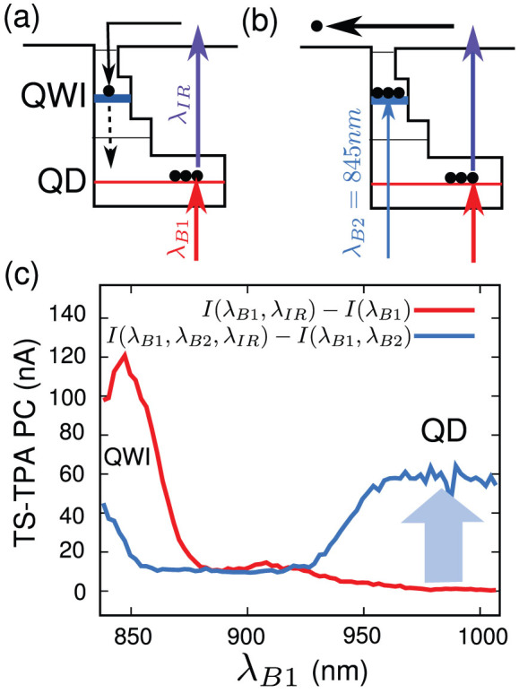
(a,b) Band diagrams illustrating the mechanism responsible for the low TS-TPA efficiencies observed experimentally. (a) QD states (red) are excited, while QWI states (blue) are hardly occupied. Hot carriers created via TS-TPA from QDs by IR illumination are immediately captured by QWIs. (b) High QWI occupation condition: carriers created by TS-TPA are extracted efficiently. (c) Experimental enhancement of TS-TPA for QD and QWI excitation. The red curve shows the TS-TPA effect due to additional IR illumination in a single wavelength scan. The PC contribution at QD energies (≈1000 nm) is almost null. The blue curve shows the TS-TPA effect due to additional IR illumination in a two-beam experiment with a variable first beam and a fixed second beam at QWI energies. A significant enhancement in the TS-TPA efficiency from the QDs is observed.
Verification with power dependence
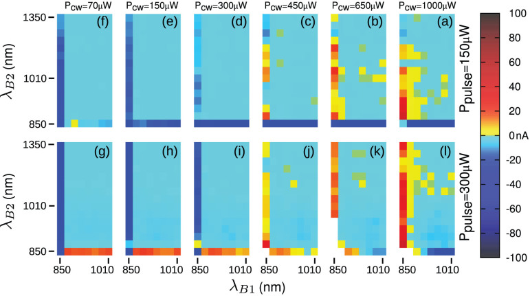
To verify that the TS-TPA efficiency is reduced by the capture of upconverted carriers in the high-energy QWI states, we investigated the power dependence of the TS-TPA map in Fig. 5d. A TS-TPA map for similar excitation conditions is shown in Fig. 7a. Region A shows a positive signal for the strong excitation of the QWIs (Fig. 7a, red vertical line; λB1 = 850 nm with PB1 = 1 mW), and region B shows a negative signal for the weak excitation of the QWIs (Fig. 7a, blue horizontal line; λB2 = 850 nm with PB2 = 150 μW). By gradually varying the B1 excitation power (a to f), the initial positive signal region begins to exhibit a negative signal (Fig. 7d–f; blue vertical line, λB1 = 850 nm).
Figure 7. Power dependence of TS-TPA effect at 30 K.
Each map is a compact representation of the TS-TPA effect in the regions A, B, and C. The PC for excitations with energies higher than the QWIs is not shown. The power of the first beam, B1 (cw), was varied from 70 μW to 1 mW in six steps, as represented by the six columns. The second beam, B2 (pulse), was used at powers of 150 and 300 μW, as represented by the two rows. The map in (a) corresponds to the TS-TPA map shown in Fig. 5 (d): positive (red) vertical data and negative (blue) horizontal data represent the TS-TPA effect in regions A and B. Figures (b)–(l) are explained in the text.
If TS-TPA occurs mainly in the QWIs, then we would expect the initial positive signal to gradually become smaller and finally zero as the excitation power decreases, since the carrier population of the QWI decreases. Therefore, the positive-to-negative change cannot be explained by TS-TPA in the QWIs. We thus concluded that the PC enhancement must be due to the PC generated via the TS-TPA process in deep QD states. Furthermore, the TS-TPA PC generation efficiency depends strongly on the carrier population of the shallow QWI states, i.e., unoccupied QWI states act as trap states and reduce the TS-TPA PC generation, but filled QWI states do not reduce TS-TPA PC generation. Hence, the sign of the signal in these regions is determined by the excitation power of the QWIs. An example is shown in Fig. 7g, where the initial positive and negative regions in (a) are inverted. By increasing the B1 excitation power (g–l) the negative branch becomes positive again. The discontinuity in the horizontal branch (j–l) and the slight negative dip in region C is explained by heating, which occurs at high power densities.
Discussion
The power dependence of the TS-TPA effect confirms that PC generation via the TS-TPA process occurs in QDs at low temperatures, and that the generation efficiency is significantly reduced by the fast recapture of photocarriers at trap states situated at higher energy levels (see Figs. 6a). This result is important for all structures containing InAs quantum structures, since the formation of such higher lying trap states cannot be prevented by using present growth techniques. The recapture of photocarriers is most likely responsible for several unexpected results reported previously. While improvement of the TS-TPA in QDs has been explored by increasing the the absorption coefficient by QD coupling or enhancing the deep IR absorption by doping of QDs, new phenomena have been observed. For example, a small additional PC due to illumination of doped QDs with low-energy photons (IR photons) was observed, but the additional PC also became stronger when the doped QDs were excited with high-energy photons (visible photons)21. Increased intraband absorption from QD states to the continuum has also been observed under high-energy photon illumination, when compared to that obtained under low-energy photon excitation31. In addition, positive as well as negative effect of doping on PC generation have been reported15,21,30,31,32; changes in the PC spectra did not reflect a definitive increase of PC contribution by TS-TPA via QDs.
There have been no consistent explanations of the results mentioned above, since the influence of states other than the QD state on the TS-TPA efficiency was not considered. However, a consistent explanation is offered by considering the recapture of TS-TPA-generated photocarriers in InAs states with an energy above the QD state. Only when these trap states are already occupied (with additional excitation or doping) or the second photon in the TS-TPA process excites the carrier to an energy level much higher than the conduction band (via TS-TPA from QDs using visible photons), recapture is avoided and TS-TPA PC generation is enhanced.
To improve the IB solar-cell efficiency we must consider the following points: The QWIs enable efficient PC generation via multicarrier Auger processes, but have a narrower absorption band than QDs and also reduce the PC generation via TS-TPA in QDs. However, a high-efficiency IB solar cell requires the use of both quantum structures to obtain broad-band upconversion with the best efficiency. Hence, a structural design that enables the most efficient upconversion in each structure without disturbing the other must be identified. Further work is required to elucidate these prospects.
In summary, we have investigated the TS-TPA efficiency in InAs QWIs and QDs using two- and three-beam experiments. Performing these experiments with two tunable sources, provides critical information about upconversion and recombination dynamics and is thus an effective approach for determining the limiting mechanism of the TS-TPA process. It has been revealed that the PC generated via TS-TPA in QDs is actually limited by the relaxation to shallow states after the absorption of the second photon. To achieve a higher TS-TPA PC contribution in IB solar cells, considering structures consisting of both QWIs and QDs is essential.
Methods
Growth
The sample structure shown in Fig. 1 was prepared by molecular beam epitaxy (MBE) and consists of an InAs layer embedded in AlGaAs and GaAs. The self-assembly of the quantum structures occurs via the Stransky–Krastanov growth mode (a strain driven growth), using either by MBE or metalorganic chemical vapor deposition. The strain due to the lattice mismatch between InAs and (Al)GaAs leads to the formation of the QWIs and QDs on top of the single-ML thick wetting layer. The ultra-thin QWIs are sometimes also interpreted as monolayer fluctuations of a rough wetting layer, but for upconversion the electronic properties of this well-defined island-structure are important and thus exact terminology is required. Details of the electronic structure of QWIs and QDs embedded in AlGaAs are explained in Ref. 16 and 17. In short, the 2 ML thick InAs/AlGaAs QWIs investigated here have a confined energy of about 1.46 eV, ≈230 meV below the AlGaAs barrier. This confinement is much shallower than those of the deep confined InAs/AlGaAs QDs, which are located at about 1.17 eV.
Sample structure
A nominally undoped sample structure was grown with MBE on top of a semi insulating GaAs (001) substrate, followed by the growth of a GaAs buffer, an AlGaAs layer including a 2 ML InAs layer (forming QDs and QWIs), and a GaAs quantum well (QW) for reference. The top of the structure was capped by a GaAs layer including a 1.4 ML InAs layer (forming only QWIs). The two InAs layers assist in determining the barrier height dependence of different upconversion mechanisms16. For the PC experiments, we used an Au contact on top and an In contact at the bottom of the structure. The applied bias voltage was below 1 V.
Measurement system
Three excitation sources (see Fig. 4) were employed: a continous wave (cw) laser (B1) tunable from λB1 = 800 to 1010 nm, a pulsed white light source in combination with a monochromator (B2) (λB2 = 800 to 1350 nm), and a cw IR laser diode (IR) with λIR = 1550 nm. In general, different excitation powers were used for B1 and B2, which is important because the effect of the modulated carrier population in different energy levels needs to be probed. Owing to the difference in carrier distribution induced by pulsed and cw excitation, small asymmetries arise in the interchanged excitation powers. The effect of pulsed excitation was verified to be minor and mainly visible as a slight reduction in the TS-TPA PC for high excitation powers due to heating.
Author Contributions
D.M.T. designed and performed experiments, analysed data and wrote the paper. Y.K. conceived the project, and Y.K. and I.K. discussed the results and wrote the manuscript.
Acknowledgments
The authors would like to thank T. Ihara for the help during the experiments. Part of this work was supported by JST-CREST; the Strategic Research Infrastructure Project of MEXT, KAKENHI (No. 25234567 and No. 25247052)).
References
- Wolf M. Limitations and Possibilities for Improvement of Photovoltaic Solar Energy Converters: Part I: Considerations for Earth's Surface Operation. Proc. IRE 48, 1246–1263 (1960). [Google Scholar]
- Swanson R. M. A proposed thermophotovoltaic solar energy conversion system. Proc. IEEE 76, 446–447 (1979). [Google Scholar]
- Barnham K. W. J. et al. Shortcircuit current and energy efficiency enhancement in a lowdimensional structure photovoltaic device. Appl. Phys. Lett. 59, 135–137 (1991). [Google Scholar]
- Werner J. H., Kolodinski S. & Queisser H. J. Novel optimization principles and efficiency limits for semiconductor solar cells. Phys. Rev. Lett. 72, 3851–3854 (1994). [DOI] [PubMed] [Google Scholar]
- Luque A. & Martí A. Increasing the Efficiency of Ideal Solar Cells by Photon Induced Transitions at Intermediate Levels. Phys. Rev. Lett. 78, 5014–5017 (1997). [Google Scholar]
- Semonin O. E. et al. Peak External Photocurrent Quantum Efficiency Exceeding 100% via MEG in a Quantum Dot Solar Cell. Science 16, 1530–1533 (2011). [DOI] [PubMed] [Google Scholar]
- Shockley W. & Queisser H. J. Detailed Balance Limit of Efficiency of pn Junction Solar Cells. J. Appl. Phys. 32, 510–519 (1961). [Google Scholar]
- Leonard D., Krishnamurthy M., Reaves C. M., Denbaars S. P. & Petroff P. M. Direct formation of quantumsized dots from uniform coherent islands of InGaAs on GaAs surfaces. Appl. Phys. Lett. 63, 3203–3205 (1993). [Google Scholar]
- Heitz R. et al. Observation of Reentrant 2D to 3D Morphology Transition in Highly Strained Epitaxy: InAs on GaAs. Phys. Rev. Lett. 78, 4071–4074 (1997). [Google Scholar]
- Kammerer C. et al. Photoluminescence Up-Conversion in Single Self-Assembled InAs/GaAs Quantum Dots. Phys. Rev. Lett. 87, 207401 (2001). [DOI] [PubMed] [Google Scholar]
- Paskov P. P., Holtz P. O., Monemar B., Garcia J. M., Schoenfeld W. V. & Petroff P. M. Photoluminescence up-conversion in InAs/GaAs self-assembled quantum dots. Appl. Phys. Lett. 77, 812–815 (2000). [Google Scholar]
- Luque A. et al. Experimental analysis of the quasi-Fermi level split in quantum dot intermediate-band solar cells. Appl. Phys. Lett. 87, 083505–083508 (2005). [Google Scholar]
- Martí A., Lopez N., Antolin E., Canovas E. & Luque A. Emitter degradation in quantum dot intermediate-band solar cells. Appl. Phys. Lett. 90, 233510–233513 (2007). [Google Scholar]
- Oshima R., Takata A. & Okada Y. Strain-compensated InAs/GaNAs quantum dots for use in high-efficiency solar cells. Appl. Phys. Lett. 93, 083111–83114 (2008). [Google Scholar]
- Guimard D. et al. Fabrication of InAs/GaAs quantum dot solar cells with enhanced photocurrent and without degradation of open circuit voltage. Appl. Phys. Lett. 96, 203507 (2010). [Google Scholar]
- Tex D. M., Kamiya I. & Kanemitsu Y. Efficient upconverted photocurrent through an Auger process in disklike InAs quantum structures for intermediate-band solar cells. Phys. Rev. B 87, 245305 (2013). [Google Scholar]
- Tex D. M. & Kamiya I. Upconversion of infrared photons to visible luminescence using InAs-based quantum structures. Phys. Rev. B 83, 081309(R) (2011). [Google Scholar]
- Luque A., Martí A. & Stanley C. Understanding intermediate-band solar cells. Nature Photon. 6, 146–152 (2012). [Google Scholar]
- Hellmann R. et al. Low-temperature anti-Stokes luminescence mediated by disorder in semiconductor quantum-well structures. Phys. Rev. B 51, 18053–18056 (1995). [DOI] [PubMed] [Google Scholar]
- Martí A. et al. Production of Photocurrent due to Intermediate-to-Conduction-Band Transitions: A Demonstration of a Key Operating Principle of the Intermediate-Band Solar Cell. Phys. Rev. Lett. 97, 247701 (2006). [DOI] [PubMed] [Google Scholar]
- Okada Y. et al. Increase in photocurrent by optical transitions via intermediate quantum states in direct-doped InAs/GaNAs strain-compensated quantum dot solar cell. J. Appl. Phys. 109, 024301–024305 (2011). [Google Scholar]
- Sauvage S., Boucaud P., Julien F. H., Gerard J.-M. & Marzin J.-Y. Infrared spectroscopy of intraband transitions in self-organized InAs/GaAs quantum dots. J. Appl. Phys. 82, 3396–3401 (1997). [Google Scholar]
- Sauvage S., Boucaud P., Gerard J.-M. & Thierry-Mieg V. In-plane polarized intraband absorption in InAs/GaAs self-assembled quantum dots. Phys. Rev. B 58, 10562–10567 (1998). [Google Scholar]
- Adawi A. M. et al. Comparison of intraband absorption and photocurrent in InAs/GaAs quantum dots. Appl. Phys. Lett. 83, 602–604 (2003). [Google Scholar]
- Popescu V., Bester G., Hanna M. C., Norman A. G. & Zunger A. Theoretical and experimental examination of the intermediate-band concept for strain-balanced (In,Ga)As/Ga(As,P) quantum dot solar cells. Phys. Rev. B 78, 205321 (2008). [Google Scholar]
- Luque A., Mellor A., Antolin E., Linares P. G., Ramiro I., Tobias I. & Marti A. Symmetry considerations in the empirical k.p Hamiltonian for the study of intermediate-band solar cells. Sol. Energ. Mat. Sol. Cells 103, 171–183 (2012). [Google Scholar]
- Tomtć S., Jones T. S. & Harrison N. M. Absorption characteristics of a quantum dot array induced intermediate-band: Implications for solar cell design. Appl. Phys. Lett. 93, 263105–263107 (2008). [Google Scholar]
- Kita T., Maeda T. & Harada Y. Carrier dynamics of the intermediate state in InAs/GaAs quantum dots coupled in a photonic cavity under two-photon excitation. Phys. Rev. B 86, 035301 (2012). [Google Scholar]
- Martí A., Cuadra L. & Luque A. Partial filling of a quantum dot intermediate-band for solar cells. IEEE Trans. Electron. Dev. 48, 2394–2399 (2001). [Google Scholar]
- Hubbard S. M. et al. Effect of strain compensation on quantum dot enhanced GaAs solar cells. Appl. Phys. Lett. 92, 123512–123514 (2008). [Google Scholar]
- Sablon K. A. et al. Strong Enhancement of Solar Cell Efficiency Due to Quantum Dots with Built-In Charge. Nano Lett. 11, 2311–2317 (2011). [DOI] [PubMed] [Google Scholar]
- Yang X. et al. Improved efficiency of InAs/GaAs quantum dots solar cells by Si-doping. Sol. Energ. Mat. Sol. Cells 113, 144–147 (2013). [Google Scholar]
- Antolin E. et al. Reducing carrier escape in the InAs/GaAs quantum dot intermediate-band solar cell. J. Appl. Phys. 108, 064513–064519 (2010). [Google Scholar]
- Seidel W., Titkov A., André J. P., Voisin P. & Voos M. High-Efficiency Energy Up-Conversion by an “Auger Fountain” at an InP-AIInAs Type-II Heterojunction. Phys. Rev. Lett. 73, 2356–2359 (1994). [DOI] [PubMed] [Google Scholar]


