We have reported recently a new scanning-probe contact-printing method, termed polymer-pen lithography (PPL),[1,2] that combines the advantages of microcontact printing (μCp)[3-7] and dip-pen nanolithography (DPN)[8-11] to achieve high-throughput molecular printing (the printing of adlayers of molecules with sub-micrometer feature size, which can chemisorb to an underlying substrate). PPL is a cantilever-free lithographic approach that uses elastomeric tips to print a digitized pattern with spot sizes ranging from 90 nm to over 10 μm in a single writing step. A typical polymer-pen array contains from thousands to as many as 107 pyramidal elastomeric tips that are made with a master prepared by conventional photolithography and subsequent chemical etching. Once the master has been prepared, the material cost of the elastomer used in each pen array is less than $1. When the sharp tips are brought into contact with the substrate, ink is delivered at these points, and a pattern is generated by repeatedly lowering the array to the surface. Because the elastomeric tip array absorbs ink and acts as a reservoir, the same polymer array can be used to print over large areas and for multiple printing tasks without reinking as long as the tips are not damaged. PPL is a promising lithographic platform, however, the ink transport mechanism from tip to surface, a property that ultimately controls many important printing parameters including feature homogeneity, feature size, and the ability to print features of different sizes and shapes, has not been investigated.
Herein, we report a study of the force- and time-dependent ink transport in PPL, and we derive a quantitative expression that relates the force applied between the tip array and the surface to the resulting feature edge length, a relationship that is unique to PPL. Specifically, we patterned 16-mercaptohexadecanoic acid (MHA) on 25-nm-thick Au films with a 5-nm Ti adhesion layer thermally evaporated on Si〈100〉/SiOx wafers. The dwell time between the inked tip array and the surface was varied using an NScriptor (NanoInk, USA) lithography platform. When contact is made between the pens and the surface, the MHA ink in the pens reacts with the Au to form a self-assembled monolayer (SAM). Upon immersion of the patterned surface in an etching solution (20 mm thiourea, 30 mm FeNO2, 20 mm HCl, and 20 mm octanol (aq)),[12] the Au is dissolved selectively from areas that are not capped by the MHA, and the resulting Au features were analyzed by scanning electron microscopy (SEM). In this study, we prepared features ranging in size from ≈500 nm to ≈4 μm with precise control over feature edge length that can be varied simply by changing the tip–substrate contact force or time, which is explained by a new model for force-dependent feature size control. Finally, we show that the application of force between the tips and substrate surface does not significantly damage the tips, so the arrays can be used repeatedly without loss of printing resolution.
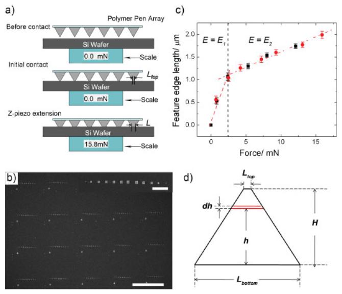
The relationship between force and feature edge length was investigated by varying the extension of the z-piezo during writing while simultaneously measuring the force and imaging the resulting features by SEM. We have shown previously a linear relationship exists between z-piezo extension and feature edge length, which has been speculated to be the result of a force-induced deformation of the elastomeric tips, but no quantitative model could be developed because the force was not measured.[1] Here, the force exerted by the tip array on the substrate during patterning was measured directly by placing a scale beneath the substrate (Figure 1a). Tips were brought into contact with the substrate so that the compression of the tips from contact with the surface could be observed optically, but no force was detected by the scale that had a sensitivity of 0.1 mN. This point was considered the z-piezo = 0 point, and all z-piezo extension values reported here are relative to this point. Patterns were written by extending the z-piezo to values from 1 to 7 μm with a dwell time of 1 s. The force exerted by the pen array on the surface was recorded during writing and the feature edge lengths were measured by SEM (Table 1, Figure 1b). To determine if there was a difference in feature size as a result of permanent deformation of the polymer pens incurred upon compressing the tips, dots were written at each value of z-piezo extension twice: once before and once after reaching a maximum z-piezo extension. Two distinct regions are observed in the plot of force versus feature size (Figure 1c): when the force is <2.5 mN, the slope of the best-fit linear regression is 0.43 μm mN −1, which is about 6 times larger than the slope of the line when a force >2.5 mN is applied (0.066 μm mN −1).
Figure 1.
a) Measurement of force during PPL writing. b) SEM images of Au features produced undervarying forces (0.7, 2.5, 4.2, 7.2, 9.3, 13.1, 15.9, 12.1, 8.0, 5.3, 2.4, 0.8, 0 mN, left to right) generated by a PPL array with ≈8000 pens. The scale bar is 80 μm. The inset is a SEM of a pattern generated from a singlepolymerpen, and the scalebar is 10 μm.c) The plot of feature edge length as a function of force between the tip and the surface. Red dots are features produced as the force is increasing and the black squares indicate features created as force is decreasing. The red dashed lines are linear fits to the data (R > 0.98 for both lines). d) Geometric model of the tip.
Table 1.
The measured and estimated feature size for different forces applied to the polymer pyramid.
|
z-piezo extension [μm] |
Force [mN] | Measured feature edge length [μm] |
Estimated feature edge length [μm] |
|---|---|---|---|
| 1 | 0.7 | 0.56 ± 0.08 | 0.36[b] |
| 2 | 2.5 | 1.04 ± 0.08 | 1.12[b] |
| 3 | 4.2 | 1.26 ± 0.07 | 1.22[c] |
| 4 | 7.2 | 1.45 ± 0.07 | 1.41[c] |
| 5 | 9.3 | 1.60 ± 0.06 | 1.56[c] |
| 6 | 13.1 | 1.77 ± 0.06 | 1.81[c] |
| 7 | 15.9 | 1.99 ± 0.08 | 1.99[c] |
| 6 | 12.1 | 1.74 ± 0.05 | 1.74[c] |
| 5 | 8.0 | 1.54 ± 0.05 | 1.47[c] |
| 4 | 5.3 | 1.30 ± 0.06 | 1.29[c] |
| 3 | 2.4 | 1.07 ± 0.08 | 1.08[b] |
| 2 | 0.8 | 0.53 ± 0.07 | 0.41[b] |
| 1 | 0 | 0[a] | 0.07[b] |
The 0-μm feature edge length means no dot is observed.
Feature edge lengths were estimated accordingto Equation (7) using N = 8000, E = 1.38 MPa, Ltop = 70 nm, and ν = 0.33.
Estimated feature edge length by using N = 8000, E = 8.97 MPa, Ltop = 70 nm, ν = 0.33, and z0 = 2.1 μm as inputs in Equation (8).
We have developed a model that relates the force between the tip array and the sample, the z-piezo extension, the mechanical properties of the polymer pens, and the geometry of the tips that explains the observed relationship between the measured force and the resulting feature edge length. In this model, the pyramid is considered to be a series of slices that allow one to model the effect of compression on the edge length of the tip, L (Figure 1d). The model assumes that in the tested z-piezo range, the deformation is completely elastic, and the elastic properties are constant over the entire pyramid (Figure 1d). This model uses the plane stress assumption that only considers stress in the direction of height and neglects the effect of strain on the pyramid side surface, which will have a negligible effect on the writing area of the deformed pyramid. Taking a slice of the pyramid that is parallel to the bottom surface of the pyramid with thickness dh, which is infinitely small, the area of the slice Sh can be calculated by
| (1) |
where Lbottom and Ltop are the edge lengths of the bottom and top surfaces of the pyramid prior to compression, h is the distance from the slice to the bottom of the pyramid, and H is the original height of the pyramid. When a force F is applied to the pyramid, Δh is proportional to the stress σ and strain εh on the slice normal to the plane of the substrate:
| (2) |
where E is the compression modulus of poly(dimethyl siloxane) (PDMS) and N is the total number of polymer pens. By integrating the changes in thickness of all the slices in the pyramid as a function of applied force, the total change in height Δh that is also equal to the z-piezo extension, Z, is described by
| (3) |
From Equation (3), Z is linearly related to F. The average feature edge length Lfeature then corresponds to the deformed pyramid top edge length:
| (4) |
where εL is the strain on the slice parallel to the surface and ν is the Poisson’s number of PDMS. However, it has been previously demonstrated that the E of PDMS depends on the compression ratio, which is described by the Mooney–Rivlin equation.[13] In our simplified model, we employ a two-stage compression modulus rather than the complete description of the Mooney–Rivlin equation. As a result, in our model (described below) there exists a threshold value of z-piezo extension, z0, below which E = E1 and above which E = E2.[14,15] This simplified two-stage model fits the experimentally observed data. The force exerted when Z ≤z0 can be described by
| (5) |
When Z > z0, the exerted force between the tip array and the surface upon z-piezo extension is described by
| (6) |
As a consequence, we can develop a new relation that describes the feature edge length for all values of F:
| (7) |
| (8) |
Importantly, from Equation (7), a value for E1 can be determined from the slope of the line corresponding to the features produced when E = E1. Additionally, Equation (8) can be used to calculate feature edge lengths as a function of F, when Z > z0 and E = E2.
To test the model, we used Equations(7) and (8) to estimate the feature edge lengths in a PPL experiment. In this exercise, experimentally determined values for F, N = 8000 for the 8000 pen array used for writing in the experiment, E2 = 8.97 MPa, ν = 0.33, and Ltop = 70 nm were used as inputs. To estimate a value for E1, a linear regression was fit to the edge lengths measured for features produced when F≤2.5 mN (Figure 1c, line with steepest slope). From the slope of this line, 0.43 μm mN −1, E1 was calculated to be 1.38 MPa from Equation (7). Another line was fitted to the feature edge lengths produced when F > 2.5 mN, from which the y-axis intercept = 0.944 μm was obtained and used to calculate z0 = 2.1 μm from Equation (8). This value of z0 corresponds to a compressive strain of 7% and is the point when E changes from E1 to E2, which is in good agreement with previous measurements on PDMS.[15] Using the above parameters, the feature edge length for each different value of F was predicted (Table 1) and found to be in good agreement with the experimentally measured features.
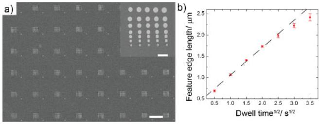
Alternatively, to investigate the relationship between dwell time and feature size in PPL, pens were brought into contact with the surface at a z-piezo extension of 2 μm, relative humidity of 50%, and tip–surface dwell times of 0.25, 1, 2.25, 4, 6.25, 9, and 12.25 s. The resulting features were measured by SEM to be 0.69±0.02, 1.07±0.02, 1.41±0.02, 1.73±0.02, 1.98±0.04, 2.22±0.05, and 2.42±0.08 mm, respectively (Figure 2a). The linear correlation between the square root of the dwell time and feature diameter confirms that PPL maintains the same relationship between dwell time and feature diameter characteristic of DPN when z-piezo extension is small and dwell time is long (Figure 2b).[1] In DPN, the meniscus that forms between the tip and the surface is a conduit for ink transport, and the feature size is a function of tip–substrate contact time, the ink coverage on the pen, and the ink diffusion coefficient. These parameters can be manipulated to form features on the sub-50-nm to many micrometer length scale.[16-19] It should be noted that at long dwell times but small force, round features result because DPN-like transport dominates ink deposition. However, at large force and short dwell times, square features are created because the force-dependent ink deposition unique to PPL determines feature shape and size. With short dwell time (0.25 s), the MHA features on the substrate are less dense than those with longer dwell time. As a consequence, during the etching process, some gold in the center of the feature is etched and a hole is left in the square feature, which is consistent with observations in the literature.[12]
Figure 2.
a) SEM image showing Au patterns generated by varying the dwell time of the tips on the surface (0.25, 1, 2.25, 4, 6.25, 9, and 12.25 s). The scale bar is 50 μm. The inset shows features generated by a single pen and the scale bar is 5 μm. b) A plot of the feature size as a function of (dwell time)1/2 has the same linear relationship characteristic of DPN. The dashed black line indicates the linear fit (R = 0.99).
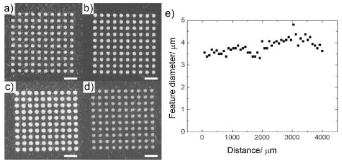
Feature homogeneity is an important parameter in parallel lithographic methods and therefore it was evaluated in the context of a PPL experiment with a 15 000-tip polymer-pen array. Within a 10 × 10 dot pattern created by a single pen with a dwell time of 0.2 s, z-piezo extension of 2 μm, and humidity of 50%, the feature size was 587±26 nm (Figure 3a–d). In addition, feature uniformity was evaluated for different writing conditions. For features with an average diameter of 1.30 μm, the standard deviation in diameter length is only 70 nm (5.4%), and for features with an average diameter of 220 nm, the standard deviation is only 15 nm (6.7%). We also compared feature uniformity for dots created simultaneously by different pens in the same polymer-pen array. The diameter of features written by different pyramids of the 15 000-pen array varied by approximately 15% (Figure 3a–e) as a result of imperfect leveling between the tip array and substrate surface.
Figure 3.
a–d) Four sets of 10 × 10 gold dot patterns produced by pens in different quadrants of the pen array, demonstrating the feature uniformity attainable across the 1-cm2 pen array. The scale bars in the figures are all 2 μm.e) Feature size of dots generated as a function of distance from one side of the pen array.
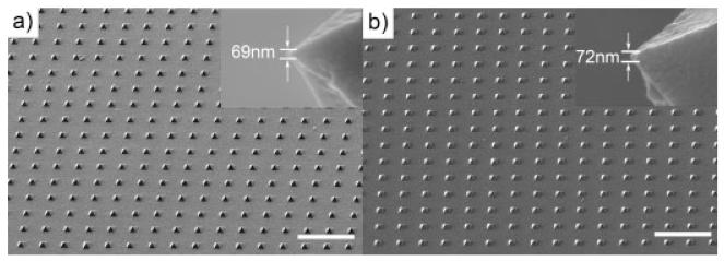
Finally, to determine whether the deformation that the pens experience during writing causes permanent damage, the pen arrays were examined by SEM before and after writing. Asingle pen array was cut into two pieces so that pens from the same array could be compared before and after writing. A 10 × 10 pattern of MHA dots was written by each pen so that each tip was subjected to 100 writing operations with 2-μm z-piezo extension, 0.2-s contact time, and 50% humidity. Subsequently, 10 nm of Pd/Pt were sputtered onto the pen arrays to make them conductive for SEM imaging and in each metal-coated pen array the top radii of 20 pens were measured (Figure 4). The average tip diameters of the pyramids that did not undergo writing was 71±14 nm, while the average diameters for the tips that were used for writing was 72±13 nm. These results indicate that the elastomeric pens are not damaged significantly during writing, the deformation that occurs during writing is fully reversible, and the pens can be reused without an increase in the resulting feature sizes over time because of tip blunting.
Figure 4.
a) SEM image of a Pt/Pd-coated tip array that was not used for writing. The inset is the SEM image of a single polymer pen. b) SEM image of the same pen array taken after 100 writing operations. The inset is the SEM image of a single polymer pen. The scale bar of both figures is 200 μm.
In conclusion, PPL is a scanning-probe contact-printing method that can be used to create patterns of sub-100-nm features with force- and time-dependent control over feature size and shape. In this study, we have developed a model that explains the dependence of feature edge length on tip-substrate force, a patterning mechanism that is unique to PPL. In addition, the uniformity of the feature sizes within a single pattern and across an entire surface has been studied quantitatively. Taken together, these data show that PPL is a facile, relatively robust molecular printing method that can be rapidly adopted by any researcher who has access to scanning-probe-microscopy equipment and moderate resolution microfabrication capabilities (for making the pen array molds).
Experimental Section
Preparation and characterization of dot arrays
Polymer-pen arrays with 8000 pens and 80-μm separation between tips were prepared and inked with MHA as previously described.[1] The polymer-pen arrays were mounted on an NScriptor (NanoInk, Inc., USA) nanolithography platform that was used for all patterning experiments. Gold nanostructures were prepared by patterning the MHA on 25-nm-thick Au films with a 5-nm Ti adhesion layer thermally evaporated on Si〈100〉/SiOx wafers (Nova Electronic Materials, USA). The tip position, z-piezo extension dwell time between the inked tip arrays and the Au surfaces, and humidity were controlled by InkCAD (NanoInk, Inc., USA) software. Upon immersion of the patterned surface in an etching solution (20 mm thiourea, 30 mm FeNO2, 20 mm HCl, and 20 mm octanol (aq)) for approximately 5 min, the Au was dissolved selectively from areas that are not capped by the MHA. The resulting Au features were analyzed by SEM (Hitachi S-4800, Japan) and a Zeiss Axiovert 200M (Carl Zeiss, Inc., Germany) optical microscope.
Variable force patterning
A scale (PS121, Ohaus, USA) was placed beneath the substrate. The MHA-inked tip arrays were brought into contact with the surface so that deformation of the pyramids could be observed optically, but no force was detected by the scale, and this point was set at z-piezo extension = 0 μm. Patterns were generated by forming dots with increasing z-piezo extensions (1–7 μm) and forming more dots while the force was decreased for each new dot (7–1 μm). Forces were determined for each different z-piezo extension and the edge lengths of 50 different features produced at each different value of z-piezo extension were measured to obtain an average feature size.
Footnotes
XL and ABB contributed equally to this work. CAM acknowledges a DARPA-SPAWAR, the AFOSR, and the NSF-NSEC program for generous support of this work. ABB is grateful to the NIH for financial support (5F32CA136148-02). We thank Fengwei Huo for suggesting the use of a scale in these experiments.
Contributor Information
Xing Liao, International Institute for Nanotechnology, 2145 Sheridan Road, Evanston, IL 60208 (USA); Department of Materials Science and Engineering, Northwestern University, 2145 Sheridan Road, Evanston, IL 60208 (USA).
Dr. Adam B. Braunschweig, International Institute for Nanotechnology, 2145 Sheridan Road, Evanston, IL 60208 (USA); Department of Chemistry, Northwestern University, 2145 Sheridan Road, Evanston, IL 60208 (USA)
Zijian Zheng, International Institute for Nanotechnology, 2145 Sheridan Road, Evanston, IL 60208 (USA); Department of Chemistry, Northwestern University, 2145 Sheridan Road, Evanston, IL 60208 (USA).
Chad A. Mirkin, International Institute for Nanotechnology, 2145 Sheridan Road, Evanston, IL 60208 (USA); Department of Materials Science and Engineering, Northwestern University, 2145 Sheridan Road, Evanston, IL 60208 (USA); Department of Chemistry, Northwestern University, 2145 Sheridan Road, Evanston, IL 60208 (USA).
References
- [1].Huo FW, Zheng ZJ, Zheng GF, Giam LR, Zhang H, Mirkin CA. Science. 2008;321:1658. doi: 10.1126/science.1162193. [DOI] [PMC free article] [PubMed] [Google Scholar]
- [2].Braunschweig AB, Huo FW, Mirkin CA. Nat. Chem. 2009;1:353. doi: 10.1038/nchem.258. [DOI] [PMC free article] [PubMed] [Google Scholar]
- [3].Kumar A, Whitesides GM. Appl. Phys. Lett. 1993;63:2002. [Google Scholar]
- [4].Xia YN, Rogers JA, Paul KE, Whitesides GM. Chem. Rev. 1999;99:1823. doi: 10.1021/cr980002q. [DOI] [PubMed] [Google Scholar]
- [5].Gates BD, Xu QB, Stewart M, Ryan D, Willson CG, Whitesides GM. Chem. Rev. 2005;105:1171. doi: 10.1021/cr030076o. [DOI] [PubMed] [Google Scholar]
- [6].Xia YN, Whitesides GM. Adv. Mater. 1995;7:471. [Google Scholar]
- [7].Delamarche E, Schmid H, Bietsch A, Larsen NB, Rothuizen H, Michel B, Biebuyck H. J. Phys. Chem. B. 1998;102:3324. [Google Scholar]
- [8].Piner RD, Zhu J, Xu F, Hong SH, Mirkin CA. Science. 1999;283:661. doi: 10.1126/science.283.5402.661. [DOI] [PubMed] [Google Scholar]
- [9].Ginger DS, Zhang H, Mirkin CA. Angew. Chem. Int. Ed. 2004;43:30. doi: 10.1002/anie.200300608. [DOI] [PubMed] [Google Scholar]
- [10].Salaita K, Wang YH, Mirkin CA. Nat. Nanotechnol. 2007;2:145. doi: 10.1038/nnano.2007.39. [DOI] [PubMed] [Google Scholar]
- [11].Banerjee D. In: Biological and Biomedical Technologies. Lee AP, Lee LJ, editors. Springer; New York: 2006. p. 265. [Google Scholar]
- [12].Geissler M, Schmid H, Bietsch A, Michel B, Delamarche E. Langmuir. 2002;18:2374. [Google Scholar]
- [13].Mark JE. Physical Properties of Polymers Handbook. 2nd ed. Springer; New York: 2006. [Google Scholar]
- [14].Hong JM, Ozkeskin FM, Zou J, Micromech J. Microeng. 2008;18:015003. [Google Scholar]
- [15].Choi KM. J. Phys. Chem. B. 2005;109:21525. doi: 10.1021/jp050302t. [DOI] [PubMed] [Google Scholar]
- [16].Jang JY, Hong SH, Schatz GC, Ratner MA. J. Chem. Phys. 2001;115:2721. [Google Scholar]
- [17].Manandhar P, Jang J, Schatz GC, Ratner MA, Hong S. Phys. Rev. Lett. 2003;90:115505. doi: 10.1103/PhysRevLett.90.115505. [DOI] [PubMed] [Google Scholar]
- [18].Weeks BL, Noy A, Miller AE, De Yoreo JJ. Phys. Rev. Lett. 2002;88:255505. doi: 10.1103/PhysRevLett.88.255505. [DOI] [PubMed] [Google Scholar]
- [19].Giam LR, Wang YH, Mirkin CA. J. Phys. Chem. A. 2009;113:3779. doi: 10.1021/jp809061e. [DOI] [PubMed] [Google Scholar]


