

Abstract
In this paper, we present a fully integrated active voltage doubler in CMOS technology using offset-controlled high speed comparators for extending the range of inductive power transmission to implantable microelectronic devices (IMD) and radio-frequency identification (RFID) tags. This active voltage doubler provides considerably higher power conversion efficiency (PCE) and lower dropout voltage compared to its passive counterpart and requires lower input voltage than active rectifiers, leading to reliable and efficient operation with weakly coupled inductive links. The offset-controlled functions in the comparators compensate for turn-on and turn-off delays to not only maximize the forward charging current to the load but also minimize the back current, optimizing PCE in the high frequency (HF) band. We fabricated the active voltage doubler in a 0.5-μm 3M2P std. CMOS process, occupying 0.144 mm2 of chip area. With 1.46 V peak AC input at 13.56 MHz, the active voltage doubler provides 2.4 V DC output across a 1 kΩ load, achieving the highest PCE = 79% ever reported at this frequency. In addition, the built-in start-up circuit ensures a reliable operation at lower voltages.
Keywords: Active voltage doubler, high speed comparators, implantable microelectronic devices, inductive power transmission, integrated rectifier, near field, offset control, radio-frequency identification (RFID)
I. Introduction
IMPLANTABLE microelectronic devices (IMD) have already been used successfully in the form of cochlear implants to substitute a sensory modality (hearing) that might be lost due to diseases or injuries [1]. More recent IMD applications demand higher performance and more power efficiency to enable very sophisticated treatment paradigms, such as retinal implants for the blind or bidirectional cortical brain-computer-interfaces (BCI) with sensory feedback for amputees or those suffering from severe paralysis [2]–[4]. These IMDs require more power to handle more functions on a larger scale, particularly when they need stimulation through a large number of electrodes at high rates, which power level is less dependent on the circuit efficiency [5]. Therefore, the new IMD power consumption is going to be orders of magnitude higher than more traditional IMDs, e.g., pacemakers [6], and supplying them with primary batteries will not be an option. Inductive power transmission across the skin is, however, a viable solution to overcome size, cost, and longevity while providing sufficient power to such IMDs [5], [7]–[9]. Considering that the temperature at the outer surface of the IMD should not increase more than 2°C for the surrounding tissue to survive [10], it is of utmost importance for the inductive link and the IMD power management circuitry to maintain very high power transfer efficiency. There are also other applications such as inductively powered wireless sensors, radio frequency identification (RFID), and near-field communication (NFC), in which the size and cost of neither primary nor secondary (i.e., rechargeable) batteries are justified, while high power efficiency and robustness even through weak inductive links are highly desired [11], [12].
Fig. 1 shows the block diagram of an inductively-powered IMD with emphasis on the inductive power transmission that consists of three main components: power transmitter (Tx), inductive link, and IMD (Rx). On the Tx side, the primary coil, L1, is driven by a power amplifier (PA) at the carrier frequency, fc. This signal induces power in the secondary coil, L2, and the active voltage doubler converts the AC voltage in L2C2 tank to a DC voltage (VOUT) at higher levels than the peak input voltage.
Fig. 1.
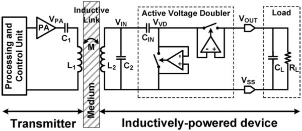
Block diagram of an inductively-powered device (e.g., an IMD) with emphasis on the inductive power transmission through the proposed active voltage doubler.
The size of L2 is significantly constrained when it is meant to be implantable in the human body or embedded in a small RFID tag, resulting in small L2 value and low VIN [13]–[15]. There are also IMDs under development, in which the secondary coil has to be embedded in the stimulator package (e.g., to be injectable) or directly implemented on the backside of the microelectrode array to facilitate the system microassembly and packaging by eliminating the flex cable that would otherwise be needed to place L2 under the skin [16], [17]. In such cases, the distance between L1 and L2 can be considerably larger than the size of L2, significantly limiting VIN. This condition renders even the most efficient rectifiers either ineffective or highly inefficient. Thus, similar to far field RFID tags in the UHF band, in order to generate the desired VOUT from a small VIN while maintaining high efficiency, a viable solution could be using voltage doublers which can operate at lower VIN,peak while providing sufficient VOUT. This can also increase the read range in the RFID tags that operate in the HF band.
Both rectifiers and voltage doublers have been widely used for inductively-powered applications. Passive rectifiers and voltage doublers using diode-connected transistors suffer from large forward voltage drops and power losses because of their threshold voltages [9], [18]–[22]. A bridge rectifier using Schottky diodes has low dropout voltage [23], but it has high leakage current and it is not available in a standard CMOS process without extra fabrication steps. In addition, its reverse breakdown voltage may not be high enough for stimulation applications. Several VTh compensation techniques have been proposed to reduce the effective VTh [24]–[29]. However, they still need to deal with several issues such as sensitivity to process variations, leakage, and back currents.
Synchronous active rectifiers have achieved high power conversion efficiency (PCE) because their pass transistors operate as switches in deep triode region with low dropout voltages [30]–[44]. However, their peak input voltages, which may be significantly limited by weakly coupled inductive links, need to be always higher than the desired output voltages, resulting in lower operating range or higher voltages on the Tx side. In order to address such limitations, comparator-based active voltage doublers have been recently proposed [45], [46]. However, these topologies only operate at low frequencies (< 1 kHz) in applications such as energy scavenging from vibrations using piezoelectric transducers. Improved voltage doublers are required for IMD and RFID applications with inductive links that operate within the HF band, such as 13.56 MHz, in the Industrial, Scientific, and Medical (ISM) band.
In this paper, we propose a fully-integrated power-efficient active voltage doubler employing high speed comparators for inductively-powered applications such as IMD, RFID, and NFC. Comparators are equipped with offset control functions to compensate for both turn-on and turn-off delays. The active voltage doubler achieves high PCE comparable to the active rectifiers while generating the desired DC output voltage with much lower AC inputs than either active rectifiers or passive voltage doublers. Section II describes the concept, operating principle, and PCE analysis of the active voltage doubler. Section III presents circuit details and design considerations including the effects of the proposed offset-control functions in high speed comparators. Simulation and measurement results are in Section IV, followed by conclusions in Section V.
II. Active Voltage Doubler Architecture
A. Operating Principle of the Voltage Doubler
Fig. 2 shows the topology of the conventional passive voltage doubler using either diodes or diode-connected transistors. It consists of one capacitor, CIN, and two diodes, DN and DP, with forward dropout voltages of VDN and VDP, respectively. Rectified output voltage, VOUT, is low pass filtered by CL, and supplies the load resistor, RL. The sinusoidal input voltage, VIN, generated across the secondary resonance circuit, L2C2, has a peak amplitude of VIN,peak, which depends on the inductive link parameters and VPA at the output of the power amplifier (PA), shown in Fig. 1 [14].
Fig. 2.

Schematic diagram of the passive voltage doubler using diodes or diode-connected transistors.
When VIN goes below −VDN, VVD is connected VSS to through DN, and CIN is charged to VIN,peak − VDN, with VVD as the positive node. When VIN increases above −VIN,peak, DN turns off again and the isolated VVD increases by following VIN,peak − VDN + VIN. When VVD > VOUT + VDP, DP turns on and current flows from VIN to VOUT to charge the RLCL load. In this step, the charge stored in CIN decreases by the amount of charge delivered to the load, but CIN is charged again to VIN,peak − VDN in the next cycle. Due to the dropout voltage across DP, VOUT can reach a maximum voltage of 2VIN,peak − VDN − VDP. The total dropout voltage of the voltage doubler, VDrop, can be calculated from
| (1) |
This equation shows that the diode dropout voltages, VDN and VDP, directly affect the voltage doubler output voltage and consequently its PCE. Thus, substituting them with fast MOS switches with low on-resistance and leakage would be an effective way of reducing VDrop and improving the PCE.
B. Implementation of the Active Voltage Doubler
Fig. 3 shows a simplified schematic diagram of the proposed active voltage doubler, in which two pass transistor switches, N1 and P1, are driven by high-speed comparators, CMPN and CMPP, respectively. When VVD < VSS, CMPN output goes high, N1 turns on with a low dropout voltage, VDS(N1), and CIN is charged to VIN,peak − VDS(N1) in the shown polarity. Similarly, when VVD < VOUT, CMPP output goes low, P1 turns on with a low dropout voltage, VSD(P1), and current flows through P1 to charge RLCL in the shown polarity. Therefore, after a few cycles, VOUT is charged up to 2VIN,peak − VDS(N1) − VSD(P1), and the total dropout voltage, VDrop = VDS(N1) + VSD(P1), which results from the instantaneous input current flowing through the on-resistance of N1 and P1, will be much smaller than that of the passive voltage doubler in Fig. 2 (VGS(N) + VSG(P)).
Fig. 3.

Schematic diagram of the proposed active voltage doubler employing high speed offset-controlled comparators, CMPN and CMPP, to drive N1 and P1 pass transistors, respectively, and achieve higher PCE.
To drive N1 and P1 at high frequencies in the order of 13.56 MHz, comparators are equipped with internal offset-control functions that are externally adjustable (CTL0:3) to reduce the effects of the comparators' delay. Also, the separated N-well body terminal of P1 needs to be connected to the highest potential on the chip to prevent latch-up and substrate leakage problems. Therefore, in Fig. 3 we have adopted the dynamic body biasing technique from [18] with auxiliary transistors, P3 and P4, automatically connecting VBODY to the highest potential between VVD and VOUT.
Since the comparators are supplied from VOUT, which is initially at 0 V, it is necessary for the active voltage doubler to have startup capability. The startup block in Fig. 3, which has been described in Section III.C, generates a complementary pair of startup enable signals, SU and SUB, depending on the VOUT level to control the startup switches, N2 and P2, as well as the comparators. When VOUT is too low to operate the comparators, the startup circuit sets SU = high and SUB = low, which turn on N2 and P2, respectively, while disabling the comparators. In this condition, both N1 and P1 are diode-connected to form a passive voltage doubler, which starts charging VOUT regardless of the comparators' status. When VOUT exceeds a certain level that is sufficient to operate the comparators, SU and SUB toggle and turn N2 and P2 off, while enabling the comparators to normally run the active voltage doubler.
C. PCE Analysis and Optimization
The PCE of the active voltage doubler can be expressed as
| (2) |
where PLoad is the power delivered to the load and PCMP is the internal power consumption of comparators excluding the power needed to drive the gates of P1 and N1. PTr.sw and PTr.Ron are the power losses in the pass transistors due to gate switching and dissipation in Ron, respectively. The sizing of P1 and N1 plays an important role in the PCE optimization since PTr.sw and PTr.Ron are affected by W and L of each pass transistor. Some of the terms in (2) can be approximated by
| (3) |
| (4) |
| (5) |
where Wp and Wn are the widths of P1 and N1, and Cgp and Cgn are the gate capacitance per unit width of P1 and N1, respectively. Fc = 13.56 MHz is the carrier frequency, and D is the operating duty cycle (see Appendix). Ip and In are currents flowing through P1 and N1, respectively, and they are assumed to be equal. We also found PCMP at each VOUT from simulations (0.1 ~ 0.8 mW), and used it in the PCE analysis. Lp and Ln are 0.6 μm, the minimum length in this process.
Even though larger widths of pass transistors decrease PTr.ron, they increase switching losses, PTr.sw, due to larger parasitic gate capacitances. Hence, each pass transistor has an optimal size for minimum power dissipation depending on several parameters, such as VOUT, RL, and fc. In the Appendix, we have derived detailed equations for the PCE and VDrop while calculating optimal sizing of pass transistors for our target specifications.
III. Circuit Details and Design Considerations
A. Offset-Controlled High Speed Comparator
CMPN and CMPP need to drive large gate capacitances of N1 and P1 at high frequencies, respectively. Thus, key design parameters are drive capability and short delay. Comparator delay can reduce the PCE by either decreasing the input power that could otherwise be delivered to the load or allowing instantaneous back currents that flow from CL back to L2C2 tank when VIN < VOUT. To reduce such delays, we have designed high-speed comparators with adjustable internal offsets, which basic concept was introduced in [44]. These built-in offset control functions help comparators turn their pass transistors on and off at proper times, leading to higher PCE.
Fig. 4 shows the schematic diagram of two symmetrical high-speed comparators, CMPN in Fig. 4(a) and CMPP in Fig. 4(b), each of which is equipped with three built-in offset-control functions. In Fig. 4(a), P7-P8, N3-N4, and P15-N7 form a common-gate comparator, which input terminals at the sources of N3 and N4 are connected to VSS and VVD, respectively. P6 and R1 form a biasing branch, which is mirrored on to P7 and P8. Thus, the comparator requires a minimum supply voltage of VTH(P6) in order to start its operation. Since the gate of the diode-connected N3 is coupled with N4, currents flowing through N3 and N4 depend on their source voltages, VSS and VVD, respectively. When VVD < VSS, the current flowing through N4 tends to be larger than that of N3, P7, and P8. Hence, V1, the input of the P15-N7 inverter rapidly drops, leading to a high comparator output voltage, VCN, which turns N1 on.
Fig. 4.

Schematic diagram showing three offset-control functions built-in our high speed comparators, (a) CMPN and (b) CMPP : Offset-1 for turn-on delay, Offset-2 for turn-off delay, and Offset-3 for reliable turn-off operation.
Even though common-gate comparators are considered high speed due to their low input impedance and simple structure, their speed of operation in our 0.5-μm process was not fast enough to drive large capacitive loads (N1 and P1) at 13.56 MHz. Therefore, we added Offset-1N and Offset-2N-inside CMPN (and their duals in CMPP) in order to compensate for the turn-on and turn-off delays, respectively. Offset-1N block is implemented using N5 current source, controlled by N6 switch, which can pull additional offset current from CMPN output branch, leading V1 to start dropping earlier when this offset mechanism is activated by VOS1N = high. Constant Offset-2N has been implemented using the size mismatch between P8 and P7. The larger W/L ratio of P8 pushes additional offset current into the comparator output branch to increase V1 early.
The offset control signal, VOS1N, is provided by an offset control block that consists of the current-starved inverter, P16-P17-N8, and other logic gates in Fig. 4(a). When VVD > VSS, VCN = low, and VOS1N = high. Thus, N6 turns N5 on to pull offset current in parallel with N4 at a level that is higher than the additional current that is pushed in P8 by Offset-2N. Therefore, VVD starts to increase earlier to turn on N1a bit before VVD falls below VSS to compensate for the comparator turn-on delay. Once VCN = high, the Offset-1N block turns off, and the offset current pushing through P8 becomes dominant. As a result, VCN starts to decrease earlier to turn N1 off a bit before VVD exceeds VSS to compensate for the comparator turn-on delay. In this case, VOS1N goes high after the delay generated by the current- starved inverter, which should be shorter than one carrier cycle period. Since switches to high when VVD is much higher than VSS, it does not cause any fluctuation or instability issues through its feedback loop.
Sudden variations in VVD may occur with rapid changes in the forward current due to interconnect parasitic inductance between L2C2 tank and the voltage doubler. These variations may disrupt proper switching of the pass transistors and should be avoided. To protect the comparators against such effects, we have added a 3rd offset branch, Offset-3N, which consists of P9 current source, controlled by P13 switch. When VCN goes low, it takes a while before the current-starved inverter output goes high. During this time, VOS3N = low, activating the Offset-3N branch to inject additional current into V1 node and prevent VCN from undesired changes due to VVD variations. This will keep N1 off until the next carrier cycle.
Fig. 5 shows the timing relationship between the input, output, and comparator voltages of the voltage doubler and the offset control signals of each comparator. All transitions of the offset control signals occur fast with negligible rising and falling times even in the gray area in Fig. 5. When the current-starved inverter delay is changed, the transitions of VOS1,3N and VOS1,3P may start earlier or later, but their rising and falling times still remain very small. V1 and V2 in Fig. 4 also have small rising and falling times. Based on simulation results, V1 starts to drop ~ 2.5 ns earlier before VVD < VSS (due to Offset-1N) and starts to increase ~ 4 ns earlier before VVD > VSS (due to Offset-2N), expediting VCN transitions.
Fig. 5.

Timing diagram showing the relationship between the operating voltages of the active voltage doubler and the offset control signals of each comparator.
It should be noted that the current-starved inverter delay does not need to be accurate, and its changes due to process variations can be tolerated as long as the delay time is terminated before the next transition time. For example, VOS1N goes low when VVD < VSS, and it should go back high again sometime after VVD > VSS and before VVD goes below VSS again in the next cycle. Therefore, the low-to-high transition of VOS1N can occur anytime during VVD > VSS. When designing comparators for this active voltage doubler, the current-starved inverter delay should be set first, and then Offset-1, -2, and -3 should to be tuned in this order by adjusting the sizes of their current source transistors because modifying each parameter can affect the timing and values of the following parameters.
In addition, we have added 4-bit off-chip digital control signals, two for each comparator, CTL0:1 (CMPN) and CTL2:3 (CMPP), which should be connected to either VOUT (high) or VSS (low), to adjust the switching times of the voltage doubler against process variations before the chip is used. For example, when CTL0 = low, the reduced current in P8 drives node V1 more weakly, delaying VCN decrement and the onset of turning N1 off. On the contrary, when CTL1 = low, P10 increases the size mismatch in the Offset-2N, VCN increases more rapidly, and N1 turns off earlier. Moreover, startup control switches, P12 and N16, are added in CMPN and CMPP, respectively, for a reliable startup operation as a passive voltage doubler. These switches turn on during the initial startup period and ensure that VCN and VCP are connected to VSS and VOUT, respectively.
B. PCE Optimization With Offset-Control Functions
To further clarify the effects of offset-control functions on the PCE, in Fig. 6(a) and (b) we have compared simulation results that show the voltage doubler input/output voltages (VVD and VOUT), comparator output voltages (VCN and VCP), and input power waveforms with the offsets disabled and enabled, respectively. In these simulations, we applied an AC voltage of VIN,peak = 2 V at fc = 13.56 MHz to the input and connected RLCL = 1 kΩ ∥ 2 nF to the output of the active voltage doubler. Fig. 6(a) shows that without offset-control functions, because of the comparator turn-on delays, VCN and VCP turn on N1 and P1 too late, respectively. This results in power conduction delays through the pass transistors, from L2C2 tank to the load, when VVD < VSS or VVD > VOUT. Moreover, comparator turn-off delays result in VCN and VCP turning off N1 and P1 too late, inducing back currents flowing from CIN to VSS and from the output load to the L2C2 tank, respectively. Both of these effects significantly decrease VOUT (= 2.4 V) and PCE (= 28%).
Fig. 6.
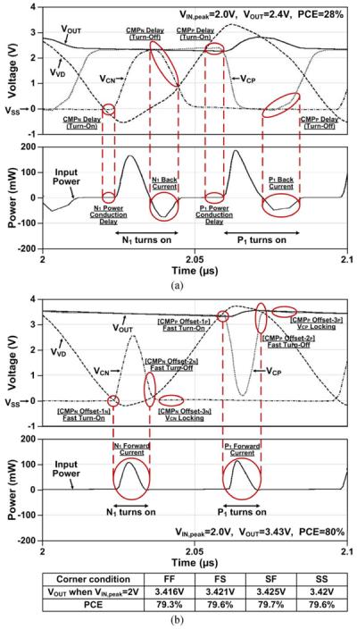
Simulation results of the active voltage doubler showing waveforms of the input/output voltages and input power with VIN,peak = 2 V, RLCL = 1 kΩ ∥ 2 nF, CIN = 2 nF, and fc = 13.56 MHz. (a) Without any offset-control functions. (b) With all three offset-control functions in the nominal and four process corner conditions.
Fig. 6(b) shows that the abovementioned conduction delays and back currents can be significantly reduced using offset-control functions utilized in Fig. 4 comparators. Offset-1 and offset-2 functions compensate for the turn-on and turn-off delays, respectively, such that VCN and VCP can turn on/off their pass transistors at the right time, leading to the highest possible PCE. Thanks to these offset-control functions, the active voltage doubler can achieve much higher VOUT (= 3.43 V) and PCE (= 80%) with the same VIN,peak and loading. Offset-3 function forces VCN and VCP to stay at VSS and VOUT, respectively, after their conduction periods in order to provide reliable pass transistor turn-off against spurious VVD variations (not shown in these simulations).
C. Self-Startup Capability
The active voltage doubler is cable of starting up before its supply rail, VOUT, is charged up to the level that is needed for the comparators to operate. The startup circuit in Fig. 7 reconfigures the doubler circuit as a diode-connected passive voltage doubler by generating SU and SUB signals based on VOUT. When VOUT = 0 V, comparator outputs, VCN and VCP in Fig. 3, are also at 0 V. In this condition, P1 and N1 are diode-connected and conduct when VVD > VTh(P1) and VVD < −VTh(N1), respectively, and VOUT starts to charge up. In Fig. 7, when VOUT < VTh(N22) + VTh(P24), P24 stays off and V3 remains at 0 V through R4. SU and SUB follow VOUT and VSS and result in N1 and P1 to stay diode-connected. During the same period, P12 and N16 in Fig. 4(a) and (b) force VCN and VCP to be low and high, respectively, further supporting N1 and P1 to be diode- connected. When VOUT > VTh(N22) + VTh(P24), N22 turns on creating sufficient voltage across R3 to turn on P24 and pull V3 up. This, SU and SUB become VSS and VOUT, respectively, turning N2 and P2 off, releasing the comparator outputs, and allowing N1 and P1 to operate as switches. Both R3 and R4 have 1 MΩ values to reduce static power consumption.
Fig. 7.
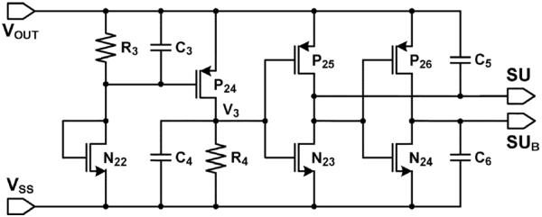
Schematic diagram of the startup circuit, which generates the startup enable signals, SU and SUB.
Fig. 8 shows the simulated waveforms for the self-startup process of the active voltage doubler, which guarantees that VOUT is charged up to about 1.4 V before resuming its normal operation. Since sub-threshold operation of transistors also conducts a small amount of currents, the startup switching voltage may practically be less than the theoretical limit of VTh(N22) + VTh(P24).
Fig. 8.

Simulation results showing self-startup capability of the active voltage doubler (VIN,peak = 1.5 V, VOUT = 2.4 V, RL = 1 kΩ, CIN = CL = 1 nF, and fc = 13.56 MHz).
IV. Simulation and Measurement Results
A. Chip Micrograph and Measured Waveforms
The active voltage doubler was fabricated in the ON Semiconductor 0.5-μm 3M2P standard CMOS process for its relatively high voltage handling capability. Fig. 9 shows the chip micrograph of the active voltage doubler, which includes comparators (CMPN and CMPP), pass transistors (N1 and P1), control switches (N2 and P2–4), and the startup circuit (SU). The active voltage doubler occupies 0.144 mm2 of silicon area with Wp/Lp = 2100 μm/0.6 μm and Wn/Ln = 1200 μm/0.6 μm. In our test setup, a class-C power amplifier drives the inductive link, which specifications are shown in Table II, to provide the active voltage doubler with 13.56 MHz sinusoidal input.
Fig. 9.

Fabricated chip micrograph and floor plan of the active voltage doubler in ON-Semi 0.5-μm Std. CMOS process, occupying an area of 0.144 mm2.
TABLE II.
Additional Active Voltage Doubler Specifications
| VTh(N) / VTh(P) | 0.75 V / 0.9 V |
| Nominal output power | 4 ~ 20 mW |
| Input capacitor (CIN) / Load capacitor (CL) | 1 μF / 1 μF |
| Output ripple (RL = 1 kΩ) | 22 mVpp |
| Comparator power consumption | 0.1 ~ 0.8 mW* |
| Primary coil diameter / Inductance (L1) | 16.8 cm / 0.88 μH |
| Secondary coil diameter / Inductance (L2) | 3.0 cm / 0.41 μH |
| Pass transistor P1 size (Wp/Lp) | 2100 μm / 0.6 μm |
| Pass transistor N1 size (Wn / Ln) | 1200 μm / 0.6 μm |
| Total area on chip | 0.144 mm2 |
From simulation
Fig. 10 shows the measured input and output waveforms of the active voltage doubler under two conditions when (VIN,peak, VOUT) = (1.46 V, 2.4 V) and (2 V, 3.2 V). Directly probing the comparator outputs induces extra loading, which results in undesired additional delays. Hence, we inferred the underlying events in the circuit by inspecting VIN and VVD = VIN + VCin. In Fig. 3 once VVD exceeds VOUT, P1 turns on, and a large current flows from the L2C2 tank to charge RLCL load. This forward current flow creates a voltage drop across the parasitic coil resistance and the interconnect inductance, resulting in a small dip in VVD. While P1 is on, VVD = VOUT + IpRop, which is fairly constant due to large CL and L2 that keep VOUT and IP constant, respectively. When P1 turns off, the charging current instantaneously stops leading to a small bump in VVD waveform following which VVD returns to its normal sinusoidal shape. Therefore, P1 and N1 switching times can be estimated from VVD variations, as shown in Fig. 10. We considered the peak voltages of VIN and VVD when P1 and N1 just turned on or off in order to measure VIN·pp (= 2VIN,peak) and VVD,peak, respectively. In these measurements, RL = 1 kΩ, CIN = 1 μF, and fc = 13.56 MHz.
Fig. 10.

Measured waveforms of key nodes in the active voltage doubler, showing VIN, VVD, VOUT, and VSS for (VIN,peakVOUT = (1.46 V, 2.4 V) and (2 V, 3.2 V) when RL = 1 kΩ, CIN = CL = 1 μF, and fc = 13.56 MHz.
B. PCE and Dropout Voltage Measurements
To consider key factors that affect the active voltage doubler performance, we measured the PCE and VDrop while sweeping 1) VOUT, 2) RL, and 3) fc. Each panel in Figs. 11 – 13 shows the calculated, simulated, and measured (in two conditions) values of the PCE and VDrop to verify the accuracy of our measurements and circuit models, while providing insight for improvements. Calculated PCE and VDrop have been derived from (1) to (5) and the active voltage doubler model in the Appendix, where the switching times are assumed to be ideal.
Fig. 11.

Measured (a) PCE and (b) VDrop versus VOUT with RL = 0.5 and 1 kΩ, CIN = CL = 1 μF, and fc = 13.56 MHz.
Simulations are post-layout and include estimations of parasitic inductances. To measure the input current, we connected a small current-sense resistor, Rsense = 10 Ω, in series with the voltage doubler input and differentially measured the voltage across it. PIN was then calculated offline by integrating the instantaneous product of the input current and voltage samples. VOUT was also measured to calculate . We also considered VDrop = VIN,pp − VOUT.
Fig. 11 shows the measured, simulated, and calculated PCE and VDrop versus VOUT for RL = 0.5 kΩ and 1 kΩ, CIN = CL = 1 μF, and fc = 13.56 MHz. In our measurements, the highest PCE was 79% achieved at VOUT = 2.4 V, which was the onset of circuit operation with 1 kΩ loading. Unlike rectifiers in which the dropout voltage stays more or less constant with the PCE generally improving with higher VOUT (see [44]), we observed increments in VDrop and reductions in the PCE with increased VOUT, which is evident in Fig. 11. These are some of the possible reasons behind this observation: First, increasing VOUT with constant RL requires higher input current, resulting in higher power loss (PTr,Rom) in the pass transistors. The power dissipation of comparators (PCMP) and gate switching (PTr,sw) also increase as the comparator supply voltage, VOUT, increases. Second, it turned out that the 2-bit offset control that we have included in each comparator was only sufficient to adjust the switching times around VOUT = 2 ~ 2.8 V. Therefore, the voltage doubler operation was not optimized for VOUT > 2.8 V, resulting in both measured and simulated PCEs in Fig. 11(a) to degrade at higher VOUT. It can be observed in Fig. 10 that P1 and N1 turn off too early when VOUT = 3.2 V, limiting the input power delivered to the load and decreasing the PCE. Third, increasing VOUT resulted in higher peaks on VIN and VVD, which were also noticeable in Fig. 10, because of larger input current variations and more prominent effect of parasitic inductance. When VVD > VOUT + VTh(P1), P1 is forced to conduct as a diode-connected transistor even after CMPP tries to turn it off (due to suboptimal timing). This forced conduction in saturation region results in more power loss in P1, and consequently lowers the PCE. Similarly, if VVD < VSS − VPN − junction, it results in substrate leakage in N1 because all NMOS body terminals should be connected to VSS in this standard CMOS process. Therefore, some portion of the input current can flow through the parasitic PN junction instead of the N1 switch, leading to additional power loss.
Calculated results in Fig. 11(a) and (b) show considerably higher PCE (86%) and lower VDrop (0.27 V) compared to both simulated and measured results. Because in the theoretical circuit model we have assumed that the comparators turn the pass transistors on/off sharply with ideal timing regardless of variations in VOUT, RL, and fc to achieve the maximum possible PCE, while the switching times in simulations and measurements are optimized for a certain operating condition, VOUT = 2.4 V, RL = 1 kΩ, and fc = 13.56 MHz.
Fig. 12 shows the measured, simulated, and calculated PCE and VDrop versus RL. In Fig. 12(a), the maximum PCE was achieved with the designated RL = 1 kΩ. As RL increases above 1 kΩ, ILoad drops and PLoad for the same VOUT decreased. Therefore, the internal power dissipation (PTr.sw + PCMP) in (2) becomes more dominant, reducing the PCE. On the other hand, when RL decreased below 1 kΩ, higher input current is required to drive the heavy load, increasing PTr.Ron and VDrop, as shown in Fig. 12(b), and resulting in the PCE to decrease.
Fig. 12.

Measured (a) PCE and (b) VDrop versus RL with VOUT = 2.4 and 3.2 V, CIN = CL = 1 μF, and fc = 13.56 MHz.
Fig. 13 shows the measured, simulated, and calculated PCE and VDrop versus fc with RL = 1 kΩ. The comparator offsets of the proposed voltage doubler were designed for operation around fc = 13.56 MHz. The PCE in Fig. 13(a) sharply decreased at higher fc because the comparator delays became too long and allowed for back current to flow from CL back to the L2C2 tank. At lower operating frequencies the PCE decreased again, though at a slower rate, due to the fixed comparator offsets and CS inverter delays leading the pass transistors to turn off earlier than they should, thus conducting smaller amount of power to the load. Fig. 13(b) shows the measured versus VDrop, fc which is also affected by the switching times. Even though VOUT and RL were fixed in all frequencies, lower PCE required higher input power to achieve the same VOUT. Therefore, VDrop increased at frequencies that had lower PCE.
Fig. 13.

Measured (a) PCE and (b) VDrop versus fc with VOUT = 2.4 and 3.2 V, RL = 1 kΩ, and CIN = CL = 1 μF.
We have measured three different chips, all of which showed similar characteristics as in Figs. 11 – 13, where the measured PCE is slightly lower than the simulated PCE due to process variations. Since the active voltage doubler has been optimized for a certain operating condition, i.e., VOUT = 2.4 V, RL = 1 kΩ, and fc = 13.56 MHz, the PCE somewhat deviates from its optimal point when the operating condition changes. However, the voltage doubler still operates properly with PCE > 74% within the range of VOUT (2 ~ 4 V) and RL (0.5 ~ 1.5 kΩ), as long as fc remains at 13.56 MHz. fc is unlikely to change, because it is often controlled externally by a crystal-based oscillator that drives the power amplifier, shown in Fig. 1. The best way to oppose such PCE deviations from the optimal point is to form another closed loop around the voltage doubler at the system level to monitor VOUT and change CTL0:3 at any operating condition via a well-defined search algorithm.
Fig. 14 shows post-layout simulated power consumption in the key components of the active voltage doubler in a pie-chart, when VIN,peak = 1.45 V, VOUT = 2.4 V, RL = 1 kΩ, CIN = CL = 1 μF, and fc = 13.56 MHz. It can be seen that 80% of the input power has been delivered to the load, while the majority of the remaining 20% dissipates in the pass transistors (N1 and P1), followed by the comparators (CMPN and CMPP). Losses in N1 (6.3%) and P1 (6.4%) are due to their Ron, which are represented in our model by PTr.Ron. Power dissipation in CMPN (2.6%) and CMPP (4.6%) include the comparators' internal power consumption as well as the switching loss, which are represented in the model by PCMP and PTr.sw, respectively. In addition, the offset-controlled functions in CMPN and CMPP consume only 29 μW and 45 μW, which are 0.4% and 0.6% of the total power consumption, respectively.
Fig. 14.

Simulated power consumption pie-chart when VIN,peak = 1.45 V, VOUT = 2.4 V, RL = 1 kΩ, CIN = CL = 1 μF, and fc = 13.56 MHz.
C. Performance Summary and Comparison
Table I benchmarks several recently reported rectifiers and voltage doublers used in various power management blocks along with the proposed active voltage doubler. In rectifiers, a major limitation is that VOUT is always less than VIN,peak, as expected. Passive voltage doublers cannot provide high PCE for the reasons discussed in Section I. Two active voltage doublers have been recently reported in the literature for energy scavenging from mechanical vibrations via piezoelectric transducers, which are designed to operate at low frequencies in the order of 100 Hz [45], [46]. Even though these active voltage doubles offer high PCE, they are not suitable for inductively powered biomedical applications, which operate at much higher frequencies through near-field inductive links. What we have presented in the last column is, to the best of our knowledge, the first active voltage doubler that can operate at 13.56 MHz in the ISM-band, providing 2.4 V of DC supply to a 1 kΩ load from a peak AC input voltage of only 1.46 V, while offering the highest measured PCE of 79%. This is made possible with the accurate timing provided by offset-controlled high speed comparators for both rising and falling slopes of the carrier signal to maximize the power delivered to the load when turning the pass transistors on, while minimizing the back currents when turning them off. Table II summarizes the specifications of the active voltage doubler and the inductive link used in our measurements.
TABLE I.
Rectifier and Voltage Doubler Benchmarking
| Publication | 2007 [23] | 2009 [32] | 2009 [33] | 2011 [44] | [47] | 2009 [28] | 2011 [29] | 2008 [45] | 2011 [46] | This work | |
|---|---|---|---|---|---|---|---|---|---|---|---|
| Technology | 0.5 μm CMOS |
0.35 μm CMOS |
0.18 μm CMOS |
0.5 μm CMOS |
Discrete (1N4148) |
0.18 μm CMOS |
0.8 μm HVCMOS |
0.35 μm CMOS |
Discrete (TLV3702) |
0.5 μm CMOS |
|
| Structure | Passive rectifier (Schottky) |
Active rectifier |
Active rectifier |
Active rectifier |
Passive voltage doubler |
VTh-cancelled voltage multiplier |
VTh-cancelled voltage doubler |
Active voltage doubler |
Active voltage doubler |
Active
voltage doubler |
|
| VIN, peak (V) | 5 | 2.4 | 1.25 | 3.8 | 2.3 | 0.8 | 11.1 | N/A | 1.2 | 1.46 | |
| VOUT (V) | 4.2 | 2.08 | 0.96 | 3.12 | 2.4 | 1.8 | 20 | 3 | 2.24 | 2.4 | |
| VCE (%)* | 84 | 86.7 | 76.8 | 82.1 | 52.2 | 56.3 | 90.1 | N/A | 93.3 | 82.2 | |
| RL (kΩ) | 2.8 | 0.1 | 2 | 0.5 | 1 | 270 | 20 | 400 | 0.1 | 1 | |
| CIN / CL (μF) | − / 0.0022** | − / 1 | − / 200 pF | − / 10 | 1 / 1 | N/A | − / 1 | N/A | − / 100 | 1 / 1 | |
| fc (MHz) | 4 | 0.2~1.5 | 10 | 13.56 | 13.56 | 13.56 | 13.56 | 200 Hz | 20 Hz | 13.56 | |
| Area (mm2) | N/A | 0.4 | 0.86 | 0.18 | N/A | 0.83 | N/A | N/A | N/A | 0.144 | |
| PCE (%) | Sim. | N/A | 87 | N/A | 87 | N/A | N/A | 90.5 | 95 | N/A | 80 |
| Meas. | 75 | N/A | 76 | 80.2 | 51 | 54.9 | N/A | > 90 | 83 | 79 | |
Voltage conversion efficiency (VCE) = VOut / (VIN,peak × multiplication factor)
On-chip capacitor. All other CIN and CL are off-chip components.
V. Conclusions
Comparator-based active rectifiers are considered the most promising solutions to achieve not only high PCE but also low dropout voltage in inductive power transmission. These AC-to-DC converters, however, need peak input voltage that should always be higher than the desired output voltage. This will limit the operation range and safe voltages of most inductively- powered devices, such as IMDs and RFID tags, which tend to have weakly coupled links. In order to overcome this limitation, we have developed a fully integrated power-efficient active voltage doubler with offset-controlled high speed comparators, which can offer high PCE and low dropout voltage comparable to active rectifiers, while increasing VOUT well above the VIN,peak. Three different offset control functions, built in the comparators, compensate for their turn-on and turn-off delays to maximize forward current to the load, while minimizing the back current. In addition, a novel startup circuit has been added to the voltage doubler to guarantee its reliable initial operation as a passive voltage doubler when VOUT = 0 V. The relationship between the active voltage doubler PCE, dropout voltage, and several power loss factors has also been analyzed to provide designers with better insight towards maximizing the PCE.
Acknowledgments
This work was supported in part by the National Institute of Health grants 1R01NS062031, 5R21EB009437, and the National Science Foundation under award ECCS-824199.
Biographies

Hyung-Min Lee (S'06) received the B.S. degree (summa cum laude) in electrical engineering from Korea University, Seoul, Korea in 2006, and the M.S. degree in electrical engineering from the Korea Advanced Institute of Science and Technology (KAIST), Daejeon, Korea, in 2008.
Since 2009, he has been with the GT-Bionics lab in the Department of Electrical and Computer Engineering, Georgia Institute of Technology, Atlanta, where he is working toward the Ph.D. degree. His research interests include analog/mixed-signal integrated circuits and power management integrated circuits for biomedical implantable systems. He has received the Silver Prize in the 16th Human-Tech Thesis Prize from Samsung Electronics, Korea, and the Commendation Award in the 4th Outstanding Student Research Award from Taiwan Semiconductor Manufacturing Company, Taiwan, both in 2010.

Maysam Ghovanloo (S'00–M'04–SM'10) was born in Tehran, Iran, in 1973. He received the B.S. degree in electrical engineering from the University of Tehran, Tehran, Iran, in 1994, the M.S. degree in biomedical engineering from the Amirkabir University of Technology, Tehran, Iran, in 1997, and the M.S. and Ph.D. degrees in electrical engineering from the University of Michigan, Ann Arbor, in 2003 and 2004, respectively.
From 2004 to 2007, he was an Assistant Professor in the Department of Electrical and Computer Engineering, North Carolina State University, Raleigh. He joined the faculty of the Georgia Institute of Technology, Atlanta, in 2007, where he is currently an Associate Professor and the founding director of the Georgia Tech Bionics Laboratory in the School of Electrical and Computer Engineering. He has authored or coauthored more than 100 conference and journal publications.
Dr. Ghovanloo is an Associate Editor of the IEEE Transactions on Biomedical Circuits and Systems and the IEEE Transactions on Biomedical Engineering. He has received awards in the 40th and 41st Design Automation Conference (DAC)/International Solid-State Circuits Conference (ISSCC) Student Design Contests. He has organized special sessions and was a member of Technical Review Committees for several major conferences, such as ISSCC and ISCAS, in the areas of biomedical circuits, sensors, and systems. He is a member of the Tau Beta Pi, the Sigma Xi, and the IEEE Solid-State Circuits Society, the IEEE Circuits and Systems Society, and the IEEE Engineering in Medicine and Biology Society.
Appendix
In this section, we calculate the PCE in (2) and VDrop in (1) using simplified voltage doubler waveforms shown in Fig. 15. In this analysis, D is the voltage doubler operating duty cycle, VCin is the voltage across CIN, and T = 1/fc is the period of one operating cycle. In this simplified model, we assume: 1) VIN (t) is sinusoidal, 2) CL and CIN are large enough to maintain VOUT and VCin almost constant during T/2, i.e., ΔV ≈ 0 V, 3) comparators turn on and off their pass transistors, P1 and N1, at ideal times and their outputs, VCP and VCN, have negligible rising and falling times, and 4) VVD,peak − VOUT = VSS − VVD,min, therefore, VCin can be expressed as VOUT/2.
Fig. 15.
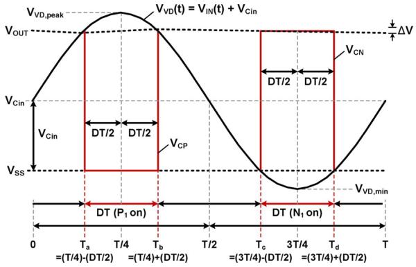
Simplified voltage waveforms of the active voltage doubler for the theoretical PCE analysis.
For this analysis, we also used the optimal size ratio ofP1 and N1 in [48] which leads to minimum Ronp + Ronn in a given area
| (6) |
While (3) and (4) can be solved directly by knowing circuit parameters, D needs to be derived to obtain PTr.Ron in (5)
| (7) |
| (8) |
The charging current flowing through pass transistors, P1 and N1, needs to be the same as the total output and dissipated currents of the voltage doubler. Therefore
| (9) |
| (10) |
In (10), VVD (t) can be written as
| (11) |
By substituting (11) in (10), D can be obtained with given values of Ronp, RL, and VOUT from
| (12) |
where PCMP and PTr,sw can be approximated from the simulation results and (4), respectively. Then, we can solve PTr.Ron in (5) using D from (12), and the PCE can be calculated by substituting (3) – (5) in (2). In addition, using MATLAB we can easily try various Ronp values (e.g., by changing Wp) and find the optimal size of the pass transistors, which results in minimum power loss and maximize the PCE. VDrop can also be estimated by obtaining VIN,peak from (11) and substituting it in (1).
References
- [1].Wilson BS, Dorman MF. Cochlear implants: A remarkable past and a brilliant future. Hearing Res. 2008 Aug;242(1–2):3–21. doi: 10.1016/j.heares.2008.06.005. [DOI] [PMC free article] [PubMed] [Google Scholar]
- [2].Shire D, Kelly S, Chen J, Doyle P, Gingerich M, Cogan S, Drohan W, Mendoza O, Theogarajan L, Wyatt J, Rizzo J. Development and implantation of a minimally invasive wireless subretinal neurostimulator. IEEE Trans. Biomed. Eng. 2009 Oct;56(10):2502–2511. doi: 10.1109/TBME.2009.2021401. [DOI] [PMC free article] [PubMed] [Google Scholar]
- [3].Ortmanns M, Gehrke M, Tiedtke H. A 232-channel epiretinal stimulator ASIC. IEEE J. Solid-State Circuits. 2007 Dec;42(12):2946–2956. [Google Scholar]
- [4].Nurmikko AV, Donoghue JP, Hochberg LR, Patterson WR, Song Y-K, Bull CW, Borton DA, Laiwalla F, Park S, Ming Y, Aceros J. Listening to brain microcircuits for interfacing with external world—progress in wireless implantable microelectronic neuro-engineering devices. Proc. IEEE. 2010 Mar;98:375–388. doi: 10.1109/JPROC.2009.2038949. [DOI] [PMC free article] [PubMed] [Google Scholar]
- [5].Ghovanloo M. Integrated circuits for neural interfacing: Neural stimulation. In: Iniewski K, editor. VLSI Circuits for Biomedical Applications. Artech House; Norwood, MA: 2008. [Google Scholar]
- [6].Haddad SAP, Houben RPM, Serdijn WA. The evolution of pacemakers. IEEE Eng. Med. Biol. Mag. 2006 May;25(3):38–48. doi: 10.1109/memb.2006.1636350. [DOI] [PubMed] [Google Scholar]
- [7].Catrysse M, Hermans B, Puers R. An inductive power system with integrated bidirectional data-transmission. Sens. Actuators A. 2004;115:221–229. [Google Scholar]
- [8].Ghovanloo M, Najafi K. A wireless implantable multichannel microstimulating system-on-a-chip with modular architecture. IEEE Trans. Neural Syst. Rehab. Eng. 2007 Sep;15(3):449–457. doi: 10.1109/TNSRE.2007.903970. [DOI] [PubMed] [Google Scholar]
- [9].Sauer C, Stanacevic M, Cauwenberghs G, Thakor N. Power harvesting and telemetry in CMOS for implanted devices. IEEE Trans. Circuits Syst. I, Reg. Papers. 2005 Dec;52(12):2605–2613. [Google Scholar]
- [10].Fujii T, Ibata Y. Effects of heating on electrical activities of guinea pig olfactory cortical slices. Eur. J. Physiol. 1982;392:257–260. doi: 10.1007/BF00584306. [DOI] [PubMed] [Google Scholar]
- [11].Finkenzeller K. RFID-Handbook. 2nd ed Wiley; Hoboken, NJ: 2003. [Google Scholar]
- [12].Near Field Communication (NFC) Forum [Online] Available: http://www.nfc-forum.org.
- [13].Baker M, Sarpeshkar R. Feedback analysis and design of RF power links for low-power bionic systems. IEEE Trans. Biomed. Circuits Syst. 2007 Mar;1(1):28–38. doi: 10.1109/TBCAS.2007.893180. [DOI] [PubMed] [Google Scholar]
- [14].Jow U, Ghovanloo M. Design and optimization of printed spiral coils for efficient transcutaneous inductive power transmission. IEEE Trans. Biomed. Circuits Syst. 2007 Sep;1(3):193–202. doi: 10.1109/TBCAS.2007.913130. [DOI] [PubMed] [Google Scholar]
- [15].Kiani M, Jow U, Ghovanloo M. Design and optimization of a 3-coil inductive link for efficient wireless power transmission. IEEE Trans. Biomed. Circuits Syst. 2011 Dec;5(6):579–591. doi: 10.1109/TBCAS.2011.2158431. [DOI] [PMC free article] [PubMed] [Google Scholar]
- [16].Harrison R, Watkins P, Kier R, Lovejoy R, Black D, Greger B, Solzbacher F. A low-power integrated circuit for a wireless 100-electrode neural recording system. IEEE J. Solid-State Circuits. 2007 Jan;42(1):123–133. [Google Scholar]
- [17].Schulman J. The feasible FES system: Battery powered BION stimulator. Proc. IEEE. 2008 Jul;96(7):1226–1239. [Google Scholar]
- [18].Ghovanloo M, Najafi K. Fully integrated wideband high-current rectifiers for inductively powered devices. IEEE J. Solid-State Circuits. 2004 Nov;39(11):1976–1984. [Google Scholar]
- [19].Sawan M, Hu Y, Coulombe J. Wireless smart implants dedicated to multichannel monitoring and microstimulation. IEEE Circuits Syst. Mag. 2005;5(1):21–39. [Google Scholar]
- [20].Ham JV, Puers R. A power and data front-end IC for biomedical monitoring systems. Sens. Actuators A. 2008 Oct;147(2):641–648. [Google Scholar]
- [21].Ghovanloo M, Atluri S. An integrated full-wave CMOS rectifier with built-in back telemetry for RFID and implantable biomedical applications. IEEE Trans. Circuits Syst. I, Reg. Papers. 2008 Nov;55(10):3328–3334. [Google Scholar]
- [22].Cong P, Chaimanonart N, Ko WH, Young DJ. A wireless and batteryless 10-bit implantable blood pressure sensing microsystem with adaptive RF powering for real-time laboratory mice monitoring. IEEE J. Solid-State Circuits. 2009 Dec;44(12):3631–3644. [Google Scholar]
- [23].Li P, Bashirullah R. A wireless power interface for rechargeable battery operated medical implants. IEEE Trans. Circuits Syst. II, Exp. Briefs. 2007 Oct;54(10):912–916. [Google Scholar]
- [24].Le T, Han J, Jouanne A, Marayam K, Fiez T. Piezoelectric micro-power generation interface circuits. IEEE J. Solid-State Circuits. 2006 Jun;41(6):1411–1420. [Google Scholar]
- [25].Umeda T, Yoshida H, Sekine S, Fujita Y, Suzuki T, Otaka S. A 950-MHz rectifier circuit for sensor network tags with 10-m distance. IEEE J. Solid-State Circuits. 2006 Jan;41(1):35–41. [Google Scholar]
- [26].Nakamoto H, Yamazaki D, Yamamoto T, Kurata H, Yamada S, Mukaida K, Ninomiya T, Ohkawa T, Masui S, Gotoh K. A passive UHF RF identification CMOS tag IC using ferroelectric RAM in 0.35-μm technology. IEEE J. Solid-State Circuits. 2007 Jan;42(1):101–110. [Google Scholar]
- [27].Kotani K, Sasaki A, Ito T. High-efficiency differential-drive CMOS rectifier for UHF RFIDs. IEEE J. Solid-State Circuits. 2009 Nov;44(11):3011–3018. [Google Scholar]
- [28].Yoo J, Yan L, Lee S, Kim Y, Yoo H. A 5.2 mW self-configured wearable body sensor network controller and a 12 μW 54.9% efficiency wirelessly powered sensor for continuous health monitoring system. IEEE J. Solid-State Circuits. 2010 Jan;45(1):178–188. [Google Scholar]
- [29].Mounaim F, Sawan M. Integrated high-voltage inductive power and data-recovery front end dedicated to implantable devices. IEEE Trans. Biomed. Circuits Syst. 2011 Jun;5(3):283–291. doi: 10.1109/TBCAS.2010.2103558. [DOI] [PubMed] [Google Scholar]
- [30].Lam YH, Ki WH, Tsui CY. Integrated low-loss CMOS active rectifier for wirelessly powered devices. IEEE Trans. Circuits Syst. II, Exp. Briefs. 2006 Dec;53(12):1378–1382. [Google Scholar]
- [31].Bawa G, Ghovanloo M. Active high power conversion efficiency rectifier with built-in dual-mode back telemetry in standard CMOS technology. IEEE Trans. Biomed. Circuits Syst. 2008 Sep;2(3):184–192. doi: 10.1109/TBCAS.2008.924444. [DOI] [PubMed] [Google Scholar]
- [32].Guo S, Lee H. An efficiency-enhanced CMOS rectifier with unbalanced-biased comparators for transcutaneous-powered high-current implants. IEEE J. Solid-State Circuits. 2009 Jun;44(6):1796–1804. [Google Scholar]
- [33].Hashemi S, Sawan M, Savaria Y. A novel low-drop CMOS active rectifier for RF-powered devices: Experimental results. Microelectron. J. 2009 Jan;40(11):1547–1554. [Google Scholar]
- [34].Lehmann T, Moghe Y. On-chip active power rectifiers for biomedical applications. Proc. IEEE Int. Symp. Circuits and Systems. 2005 May;:732–735. [Google Scholar]
- [35].Guilar NJ, Amirtharajah R, Hurst PJ. A full-wave rectifier with integrated peak selection for multiple electrode piezoelectric energy harvests. IEEE J. Solid-State Circuits. 2009 Jan;44(1):240–246. [Google Scholar]
- [36].Peters C, Spreemann D, Ortmanns M, Manoli Y. A CMOS integrated voltage and power efficient AD/DC converter for energy harvesting applications. J. Micromech. Microeng. 2008 Oct;18(10):104005. [Google Scholar]
- [37].Hwang Y, Lin H. A new CMOS analog front end for RFID tags. IEEE Trans. Ind. Electron. 2009 Jul;56(7):2299–2307. [Google Scholar]
- [38].Man TY, Mok PKT, Chan MJ. A 0.9-V input discontinuous-conduction-mode boost converter with CMOS-control rectifier. IEEE J. Solid-State Circuits. 2008 Sep;43(9):2036–2046. [Google Scholar]
- [39].Sackinger E, Tennen A, Shulman D, Wani B, Rambaud M, Lim D, Larsen F, Moschytz GS. A 5-V AC-powered CMOS filter-selectivity booster for POTS/ADSL splitter size reduction. IEEE J. Solid-State Circuits. 2006 Dec;41(12):2877–2884. [Google Scholar]
- [40].Lee E. A timing controlled AC-DC converter for biomedical implants. Proc. IEEE Int. Solid-State Circuits Conf. Dig. Tech. Papers. 2010 Feb;:128–129. [Google Scholar]
- [41].Li Q, Zhang R, Huang Z, Inoue Y. A low voltage CMOS rectifier for wirelessly powered devices. Proc. IEEE Int. Symp. Circuits and Systems. 2010 May;:873–876. [Google Scholar]
- [42].Bawa G, Huang A, Ghovanloo M. An efficient 13.56 MHz active back-telemetry rectifier in standard CMOS technology. Proc. IEEE Int. Symp. Circuits and Systems. 2010 May;:1201–1204. [Google Scholar]
- [43].Lee E. High-voltage rectifier and voltage doubler in conventional 0.18 μm CMOS process. Proc. IEEE Int. Symp. Circuits and Systems. 2010 May;:605–608. [Google Scholar]
- [44].Lee H, Ghovanloo M. An integrated power-efficient active rectifier with offset-controlled high speed comparators for inductively-powered applications. IEEE Trans. Circuits Syst. I, Reg. Papers. 2011 Aug;58(8):1749–1760. doi: 10.1109/TCSI.2010.2103172. [DOI] [PMC free article] [PubMed] [Google Scholar]
- [45].Dallago E, Miatton D, Venchi G, Bottarel V, Frattini G, Ricotti G, Schipani M. Active autonomous AC-DC converter for piezoelectric energy scavenging systems. Proc. IEEE Custom Integrated Circuits Conf. 2008 Sep;:555–558. [Google Scholar]
- [46].Cheng S, Jin Y, Arnold D. An active voltage doubling ac/dc converter for low-voltage energy harvesting applications. IEEE Trans. Power Electron. 2011 Aug;26(8):2258–2265. [Google Scholar]
- [47].1N4148WT Data Sheet, Diodes Inc. [Online] Available: http://www.diodes.com/datasheets/ds30396.pdf.
- [48].Bawa G, Ghovanloo M. Analysis, design and implementation of a high efficiency fullwave rectifier in standard CMOS technology. Analog Integr. Circuits Signal Process. 2009 Aug;60:71–81. [Google Scholar]