Abstract
Transparent ultraviolet (UV) ZnO thin film photoconductors are expected to have great applications in environmental monitoring, large-area displays, and optical communications, and they have drawn enormous interests in recent years. However, at present their performances are not satisfactory: the responsivity R (a parameter characterizing the sensitivity of the device to light) is not high (<1.0 × 10³ AW−1), and the transparency T is not high either (<80%). Realizing high R and high T remains a big challenge today. In this paper, by employing solution-processed ultrathin ZnO/Au nanoparticle composite films, R as high as 1.51 × 10⁵ AW−1 and T of over 90% are achieved. High values for detectivity D* and linear dynamic range LDR are also obtained, which are 2.05 × 10¹⁵ Jones and 60 dB, respectively. Moreover, such high-performance devices can be fabricated on flexible PET (polyethylene terephthalate) substrates.
Fully-visible transparent ultraviolet (UV) thin film photoconductors have great application potential in environmental monitoring, large-area displays, and optical communications, and they are of great importance in both civilian and military fields1,2. For an ideal visibly-blind UV thin film photoconductor, it should display high light response capability in the UV region, good linearity of the photocurrent versus incident optical power and good visible rejection (i.e., high spectral selectivity). Structural simplicity, low-cost fabrication and room-temperature operation are also crucial for real applications. In material selection, nitride compounds and metal oxides, which are wide-bandgap (larger than 3 eV) semiconductors, are considered ideal ones for high-performance UV photoconductors2,3,4.
ZnO, which is environment-friendly and has a room-temperature bandgap of 3.2 eV, is emerging as an important material for the next generation UV photoconductors for the following two main reasons: (1) There are various synthetic methods and diverse processing technologies to fabricate ZnO. (2) Oxygen molecules can adsorb on the ZnO surface and form a low-conductivity depletion layer, in which exist surface oxygen-related deep hole-trap states5,6,7,8,9,10. In a ZnO based thin film photoconductor, the oxygen-related hole-trap states can prolong the photocarrier lifetime, while the carrier transit time (between the two electrodes of the device) can be reduced by improving the electron mobility in the ZnO film (by enhancing the quality of the ZnO film). Based on the fundamental knowledge of a photoconductor device, the two important device parameters, photogain (G) and responsivity (R), are both proportional to the carrier lifetime and inversely proportional to the carrier transit time, thus the reduced carrier transit time and the prolonged carrier lifetime both play positive roles in enhancing G and R, and hence the device performance. It is also clear here that increasing electron mobility and enlarging the surface depletion layer are two efficient ways in improving the performance of a ZnO based thin film photoconductor.
In the past decades, many efforts have been done to develop high-performance ZnO based thin film photoconductors11,12,13,14,15,16. In the early days, Liang et al. presented their ZnO film based photoconductors, which exhibited a R value of of 1.5 AW−114. Such small R is resulted from both the low electron mobility (induced by the poor quality of the ZnO film) and insufficient depletion layer (induced by the small surface-to-volume ratio of the ZnO film). Later, most work concentrated on enhancing the surface-to-volume of ZnO (to enlarge the depletion area) by using nanostructured ZnO film, and the performance was indeed improved. For instance, Jin et al. have reported the ZnO nanoparticle based photoconductor, which showed a R value of 61 AW−1 15, and recently Zhu et al. reported their electron-spun ZnO-nanofiber based photoconductor with a high R value of 790 AW−1 16. However, the unavoidable nanoscale networks formed in the nanostructured ZnO film would seriously weaken the carrier mobility (because the ZnO nanostructures will not only increase the distance carrier travels between the two electrodes, but also will trap carriers at boundaries between them), which would severely limit the improvement of the R value. For example, it was reported that ZnO nanoparticle film showed an electron mobility of only 5 × 10⁻⁴ cm2V−1s−1 15,17. Additionally, the nanostructures may produce strong scattering for incident light and affect the light transmission in the visible light range15,16, and hence reduce the device transparency. For example, the electron-spun ZnO-nanofiber based film exhibits only about 75% optical transmittance (T) in the visible light range16. Therefore, realizing high T and high R ZnO based thin film photoconductor still remains a challenge today.
Results
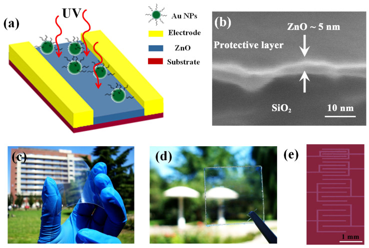
In this paper, a composite film consisting of ultrathin ZnO film (≈5 nm) and Au-DT nanoparticles (Au NPs) is applied to realize photoconductors with high R and high T (seen in Figure 1a). The continuous ZnO film exhibits high electron mobility of over 1.0 cm2V−1s−1. Moreover, the surface-to-volume ratio of the ultrathin ZnO film is quite large: The O2 related depletion layer on ZnO surface is estimated to be about 1–3 nm18, which means that the depletion region is already quite sufficient for the 5 nm ultrathin ZnO film. The Au NP put on the surface of the ZnO film leads to the formation of a localized Schottky junction, which creates a ZnO depletion region in the vicinity of the Au NP. This will further enhance the already existing O2 related depletion layer. Thus, the Au NPs can play important roles in reducing the dark current, enhancing the sensitivity and improving the response speed of the ZnO based thin film photoconductors19,20. The very small amount of the Au NPs with small sizes (2–4 nm in diameter) on the ZnO film have negligible absorption, reflection/scattering for the incident visible light. As a result, the ultrathin ZnO film itself shows a high T exceeding 96% while the final device shows a high T of over 90% (in the visible light range). R value as high as 1.51 × 10⁵ AW−1 is achieved in the UV region.
Figure 1.
(a) Schematic illustration, (b) cross-sectional SEM image, (c) device flexibility, (d) device transparency and (e) patterned ITO electrodes on the substrate of the fabricated UV photoconductor (L = 50, 100, 150, and 200 μm, W = 5000 μm).
Figure 1b presents the cross-sectional scanning electron microscopy (SEM) of our solution-processed ZnO film (the white line) used in device fabrication. It is seen that the film thickness is about 5 nm. The flexibility and transparency of our fabricated devices are clearly demonstrated in Figure 1c (PET substrate) and Figure 1d (glass substrate). The optical microscope photograph of the patterned ITO electrodes used in our photoconductors is given in Figure 1e (the light blue lines).
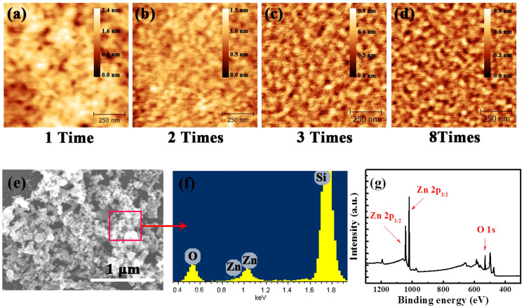
The surfaces of the individual ZnO films deposited 1, 2, 3 and 8 times (will be called 1T, 2T 3T, 8T ZnO later (seen in Methods part)) were studied by atomic force microscopy (AFM) and the morphologies are given in Figure 2a–d. It is seen that the deposition cycle affects the film morphology, the surface roughness is reduced from 0.38 nm for the 1T ZnO film to 0.21 nm for the 2T ZnO film, and then it almost remains unchanged for the 3T and the 8T ZnO films (Figure S1). In order to gain more information about the films, SEM experiments were conducted. The SEM images of the 3T ZnO film are given in Figure 2e and S2. Combining AFM and SEM image, it can be concluded that the surface of the ZnO film is consisted of small grains, which can result in a large surface-to-volume ratio. The compositions of these grains can be identified by the energy dispersive spectrometer (EDS) and the X-ray photoelectron spectroscopy (XPS) measurements. The EDS spectra (Figure 2f) and core level XPS spectra (Figure 2g and Figure S3) are both overwhelmingly dominated by the Zn and O peaks (the strong Si peak is from the SiO2 substrate). Figure S3, which is an enlarged figure of Figure 2g, provides detailed information about the Zn 2p and O 1s. The Zn 2p3/2 peak is located at 1021.27 eV and the Zn 2p1/2 peak is located at 1044.47 eV. The first O 1s peak is located at 530.37 eV, which corresponds to O atoms in ZnO. The second O 1s peak is located at 532.22 eV, which is attributed to oxygen-deficient component (for example, zinc hydroxide, Zn(OH)2). The results are in well agreement with the XPS spectra of ZnO obtained by other research groups21,22.
Figure 2.
(a), (b), (c) and (d) are the AFM images of the ZnO films formed with different deposition cycles. (e)SEM image, (f)EDS measurement and (g)XPS analysis of the ZnO film.
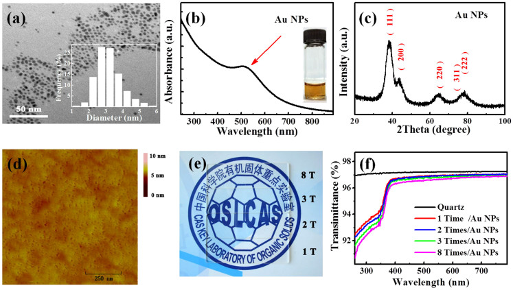
The synthesized Au NPs are studied by transmission electron microscopy (TEM), absorption and X-ray Diffraction (XRD), shown in Figure 3a, b and c, respectively. These results clearly demonstrate that the purity of the Au NPs is very high (Figure 3c), and they are very small and uniform (Figure 3a and b), with diameters in a very narrow range of 2–4 nm (inset in Figure 3a). We also performed AFM measurement on the Au NPs spin-coated on the ultrathin 3T ZnO film, the height image and phase image are given in Figure 3d and Figure S4a, respectively. From the two images it is clearly seen that the Au NPs are sparsely distributed on the ZnO film, and they only cover a very small fraction of the whole surface of the ZnO film.
Figure 3.
(a) TEM image, (b) absorption spectrum and (c) XRD pattern of the Au NPs. (d) AFM image of the as-cast Au NPs on ZnO film. (e) Photograph of four highly transparent ZnO/Au NPs films on quartz substrate, (f) UV-Vis transmission spectra. The inset in (a) is the Au NPs size histograms and that in (b) is the Au NPs solution.
The optical transmission properties the ZnO films (1T to 8T) on quartz substrates without and with the Au NPs on top are investigated by the UV-vis transmission measurements. The transmission properties of the quartz substrate (Tquartz) itself is also measured to extract the pure transmission properties of the ZnO films (TZnO = TZnO/quartz − Tquartz). TZnO and TZnO/quartz are given in Figure S4c and Figure S4d, respectively (Tquartz is provided in Figure S4d). It is seen from these figures that for all the samples, the transparency is very high with T value larger than 96% in the visible range (400–800 nm), and T value larger than 90% at low wavelength regions (<400 nm). The high T is obviously originated from the ultrathin nature of the films. Although the surface plasmon in the Au NPs can couple with incident light, producing strong scattering and absorption of incident light23,24,25, the Au NPs have negligible influence in the T value. This can be clearly seen by comparing Figure S4d and Figure 3f, in which transmission properties of the ZnO films with Au NPs are given with almost the same transparency of >96% in the visible range (400–800 nm) and of >90% in the lower wavelength range (<400 nm). The high transparencies of the ZnO films with Au NPs are also clearly demonstrated in Figure 3e, which is an optical photograph of the 1T, 2T, 3T, 8T ZnO/Au NPs films on a underlying logo.
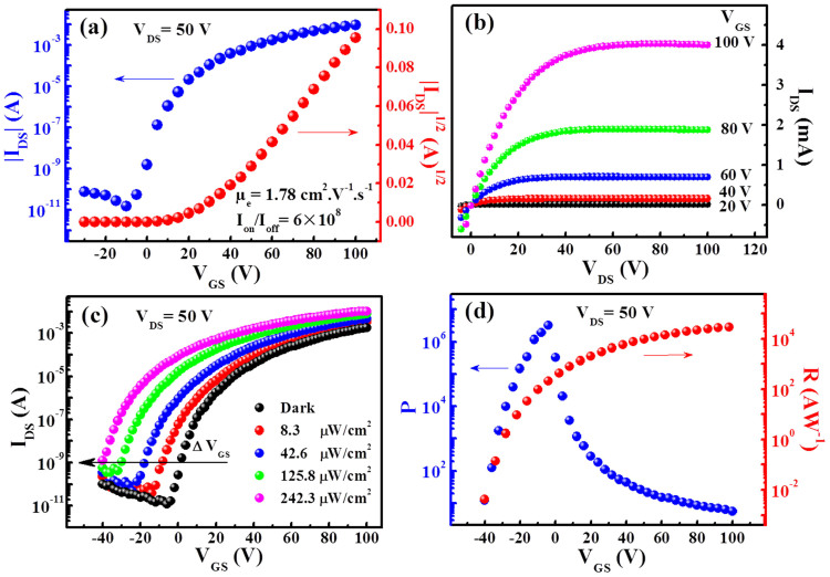
We performed XRD measurements on the four ZnO films with Au NPs (Figure S5a) aiming to relate the possible crystal nature to their electronic properties, however no XRD peak shows up in the spectra except the one from the quartz substrate. The absence of XRD peak should be that the films are too thin to give any detectable XRD signals. Field effect transistors (FETs) are fabricated for the four ZnO/Au NPs films, and their transfer curves are given in Figure S5b. It is seen that 1T ZnO/Au NPs film does not show any field effect. This could be induced by the discontinuous nature of the 1T ZnO film (seen AFM image in Figure 2a), 2T, 3T and 8T ZnO/Au NPs films all show good field effect performances, which should be induced by the high-quality continuous nature of the three ZnO films (see AFM images in Figure 2b, c and d). We also fabricated FETs with the 1T, 2T, 3T, 8T ZnO films without Au NPs on top, and their performance are very similar to that of the corresponding devices with the ZnO/Au NPs films. The 3T ZnO/Au NPs film exhibits FET performance better than the 2T ZnO/Au NPs film, but very close to that of the 8T ZnO/Au NPs film. Thereby in later study we only perform investigation on devices based on the 3T ZnO/NPs film. The transfer curve and output curve of the FET based on the 3T ZnO/Au NPs film are shown in Figure 4a and b, respectively. The device has an electron mobility of 1.78 cm2 V−1s−1 and an on/off ratio of 6 × 10⁸. The mobility was calculated based on the following equation:
 |
Where IDS is the drain current, Ci is the capacitance per unit area of the gate dielectric layer, μ is the carrier saturation mobility, W and L are the channel width and channel length (here they are 2000 and 50 μm, respectively), VGS and VT are the gate voltage and threshold voltage respectively.
Figure 4.
(a) Transfer and (b) output characteristics of the 3T ZnO/Au NPs FET (L = 50 μm, W = 2000 μm). (c) Transfer characteristics of the device in dark and under white light illumination with various intensities. (d) P and R versus VGS under white light illumination with a power of 242.3 μWcm−2.
We studied the light response capability of the 3T ZnO/Au NPs FET by illuminating the device with white light, and the results are given in Figure 4c. It is seen that the drain current increases dramatically when the device is under a very weak light illumination (8.3 μWcm−2), and the current increases with the light intensity (transfer curve moves upwards). For a photodetector device, R and signal to noise ratio (P) are two key parameters to characterize its performance26. R is defined by the following equation:
 |
Where ILight is drain current under the illumination, IDark is drain current in dark, Pill is the incident illumination power on the effective area (channel area). P is expressed by the following equation:
 |
Based on the Equation (2) and (3), we calculated R and P of the phototransistor device under white light illumination with an intensity of 242.3 μWcm−2, and they are shown in Figure 4d. For a practical photodetector, the device should keep both high P and R. Thus, the region around the crossing point of two curves can be chosen as the useful workable region. In our ZnO FETs based phototransistor, the crossing point is close to the VG = 0 V (with high R value of around 440 AW−1 and high P value of 6 × 10⁴), which is very good for practical application because only a very small applied voltage is needed.
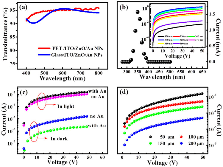
We fabricated 3T-ZnO based photoconductors on commercial PET and Glass substrates with patterned 120 nm-thick ITO electrodes, which are shown in Figure 1c and d, respectively (The ITO electrodes are given in Figure 1e). The transparencies of the final devices based on the 3T ZnO/Au NPs films are demonstrated in Figure 5a. The T values of the two devices are both larger than 90% in the visible light range (400 to 800 nm). The transparencies of the two devices in the lower-wavelength range (<400 nm) are very poor due to the light absorption by the thick ITO and PET/glass substrates (not shown). The devices also show high spectral selectivity, which can be clearly seen in Figure 5b, where the spectral response for the device on glass substrate is shown as a representative (under a light illumination intensity of 10. 6 μWcm−2 and a bias of 50 V). Figure 5c shows the dark and light I-V curves of one device based on the bare 3T ZnO film and another device based on the 3T ZnO/Au NPs film (under a light illumination intensity of 10. 6 μWcm−2). It is seen that the dark current (off current) of the 3T ZnO/Au NPs device is about 10 times lower than that of the 3T ZnO device, but its light current is about 3 times higher than that of the 3T ZnO device. The lower off current and higher light current are both induced by the enhanced depletion layer on the ZnO surface resulted from the Au NPs, as already mentioned in the introduction part. For the 3T ZnO/Au NPs film, we also investigated the device performance dependence on the channel length L (the distance between the two electrodes) by varying it from 50 to 200 μm. The I-V curves of these devices are presented in Figure 5d, it is seen that the light current decreases with increasing the channel length L. This is because longer channel length will prolong the carrier transit time from one electrode to another electrode, and fundamentally G and R and hence light current are all inversely proportional to the channel length L (which will be described in equations shown later). The shortest channel length L of the patterned ITO electrode we used here is 50 μm, but it is clear that the device performance will be further improved if the channel length can be further shortened.
Figure 5.
(a) Optical transmittances of the photoconductors. (b) Spectral R of the photoconductor based on the 3T ZnO/Au NPs film (L = 50 μm, V = 50 V), the inset shows the response of I-V curve to illumination light wavelength (10.6 μWcm−2). (c) I-V curves of the photoconductors (with and without Au NPs) in dark and under 350 nm UV light illumination with an intensity of 10.6 μWcm−2 (L = 50 μm); (d) I-V curves of the photoconductors (with Au NPs) with different channel lengths under 350 nm UV light illumination (10.6 μWcm−2).
For a photoconductor, R and G are two important parameters, and R can be expressed by the following equation27:
 |
Where EQE is the external quantum efficiency, λ is the wavelength of interest, q is the electron charge, h is the Planck constant and c is the speed of light. G is defined as the ratio between the number of electrons collected per unit time and the number of absorbed photons per unit time, and can be expressed by the following equation:
 |
Where μn is the electron mobility, μp is the hole mobility, τ is the photo carrier lifetime, E is the electrical field, L is the device channel length, tn is the electron transit time, tp is the hole transit time. From the Equation (4) and (5), it is seen that light response can be improved by enhancing the photo carrier lifetime τ and reducing the carrier transit time tn/tp. In our photoconductor, the electron mobility μn is high (and hence electron transit time tn will be small), and the photo generated holes will migrate into the depletion region induced by O2 and the Au NPs on the ZnO surface, and are then trapped there, largely preventing them from recombining with photo generated electrons. The much suppressed recombination will greatly enhance the carrier lifetime τ. Based on equation (5), the high electron mobility μn and long carrier lifetime τ would result in high G, and hence high R (equation (4)), although the light absorption of our device (<4% at a wavelength of 350 nm) is quite poor due to its ultrathin nature. This is proved by the experiment results. High G and high R are indeed obtained.
Another two figure of merits for evaluating the photoconductor performance are the detectivity (D*, in units of Jones to characterize the sensitivity) and the linear dynamic range (LDR, typically quoted in dB to measure the photosensitivity linearity). The D* can be expressed by the following equation:
 |
Where S is the effective area under illumination, q is the electron charge, IDark is the dark current. LDR is given by the following equation28:
 |
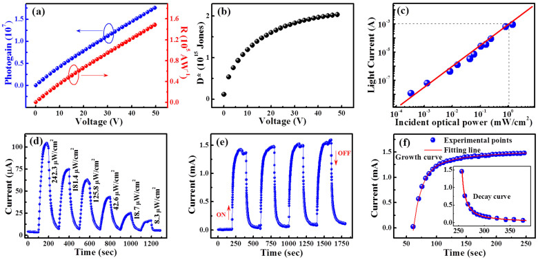
Where JLight is the photocurrent with a light intensity of 1 mWcm−2, JDark is the dark current. Based on equation (2) and the experiment results shown in Figure 5, we calculated R value of the 3T ZnO/Au NPs device, and then calculated G value of the device based on equation (4). The calculated R and G as a function of voltage are shown in Figure 6a. Based on equation (6), D* values are calculated, and they are shown in Figure 6b. G, R and D* for the photoconductor under a bias of 50 V (λ = 350 nm with power density of 10.6 μWcm−2) are 1.77 × 10⁷, 1.51 × 10⁵ AW−1 and 2.05 × 10¹⁵ Jones, respectively. Such performance is much better than that of previously reported ZnO based thin film UV photoconductors, whose performances are already described in the introduction part of this paper. Figure 6c shows the photocurrent versus the white light intensity for the device, from which LDR can be calculated based on equation (7), the calculated LDR is 60 dB of intensity linear dynamic range, a value typically required for most imaging applications29.
Figure 6.
The 3T ZnO/Au NPs photoconductor (L = 50 μm): (a) Calculated photogain and R and (b) calculated D* under 350 nm UV light illumination (10.6 μW/cm2). (c) LDR measured under white light. (d) Current versus time under various white light illumination intensities under a bias of 50 V. (e) On-off switching properties measured under 350 nm UV light illumination (10.6 μWcm−2) under a bias of 50 V. (f) Time resolved photocurrent: rise and decay (inset) curves.
Figure 6d shows the photocurrent as a function of time under white light illumination with different intensities for the 3T ZnO/Au NPs photoconductor (under a bias of 50 V). It can be clearly seen that the photocurrent responses sensitively to the illumination light intensity. In Figure 6e, the on-off switching properties of the device is shown under light illumination with 350 nm wavelength (under a bias of 50 V and illumination intensity of 10.6 μWcm−2) with both on and off time are 200 s, it is seen that the device exhibits good on-off switching performance. We also show the time-resolved photocurrent response of the device in Figure 6f. Upon illumination, the current of the device rises within 2 s. The rapid photocurrent rise is followed by a slower component, in which the photocurrent keeps increasing for about 40 s before saturation. After the light is turned off, the photocurrent drops rapidly in the first 3 s, followed by a slow decay process of more than 56 s before it returns to its initial current in dark. Such rise and decay responses can be described and fitted by equations (8) and (9), respectively:
 |
 |
Where IDark is the dark current, A and B the scaling constants, t is the time when the light was turned on or off, and τ1 and τ2 are the time constants. The two equations are widely used to analyze the photocurrent rise and decay processes of a photoconductor device30,31,32. By fitting the experiment data with the two equations, the time constants for rise and decay can be estimated. Here for our device, the estimated time constants for the rise process are: τ1 = 10.3 s, τ2 = 70.6 s. And the time constants for the decay process are: τ1 = 14.2 s, τ2 = 72.3 s. τ1 (in both rise and decay processes) should be related to the carrier generation and recombination processes in the ZnO thin film, and τ2 (in both the rise and decay processes) should be mainly related to hole trapping and release processes in the depletion layer on the surface of the ZnO film.
Discussion
In conclusion, by employing solution-processed ZnO ultrathin film and solution-processed Au NPs, high-performance UV photodetectors are fabricated. Due to the high electron mobility (over 1.0 cm2V−1s−1) exhibited by the ZnO film and the depletion layer deepening effect induced by the Au NPs on top of the ZnO film, these ZnO based UV photoconductors exhibit R values as high as 1.51 × 10⁵ AW−1 and D* values as high as 2.05 × 10¹⁵ Jones in the UV region. The ultrathin nature of the ZnO film (≈5 nm) and the ultrasmall sizes of the Au NPs (2–4 nm in diameter) render the ZnO/Au NPs films and the final devices (On PET and Glass substrates) highly transparent: The films and the photoconductors show extremely high T (transmittance) values of exceeding 96% and 90%, respectively. The devices fabricated on PET substrates display high flexibility, which are very important in real applications. We also demonstrate that by shortening the channel length, the device performance could be further improved. Our results indicate that the approach we used here is very useful in fabricating high-performance ZnO based thin film UV photoconductors.
Methods
Material preparation
All of the materials were purchased from Sigma-Aldrich and were used as received without further purification. The polyethylene terephthalate (PET), Corning Eagle XG glasses and N-doped silicon with 300 nm silicon dioxide were used as the substrates. It should be noted that the ITO electrodes of 50, 100, 150 and 200 μm in channel length and 5000 μm in channel width were patterned on the PET and Glass substrate.
Au-DT core-shell nanoparticles preparation
The Au NPs were prepared by the two-phase arrested growth method33. We dissolved 0.62 g HAuCl4·× H2O in 50 ml water and mixed it with 3 g tetraoctylammonium bromide dissolved in 160 ml p-xylene solution. The organic phase was isolated, and 0.8 ml was added. The formation of the Au NPs were completed by adding 50 ml aqueous solution of 0.76 g NaBH4 drop wise into the organic solution under vigorous stirring. The Au NPs were purified by washing with 300 ml methanol at least three times and result in a narrow size distribution (2–4 nm in diameter).
Solution ratio and concentration
Zn ammonium complex solution was prepared by dissolving ZnO hydrate in ammonium hydroxide (28–30%) to molar concentration 0.06 M. As-prepared solutions were then stirred rigorously at room temperature for 8 h. This process yielded a clear transparent solution. The Au NPs solution was prepared by dissolving 0.05 wt% Au NPs into a dichloromethane solution. The solution was stirred for ca. 24 h at 40°C.
Device fabrication
The ZnO thin film was solution-processed as described in reference 34.The as-prepared Zn ammonium complex precursor was spun onto the substrates (PET or Glass with patterned ITO electrodes) at 3000 rpm for 30 sec in air, followed by thermal annealing for 1 h at 180°C in N2. The ZnO film deposition cycle can be carried out multiple times (n times, n is the number of the deposition cycle used) in order to obtain different ZnO films for the investigation, the resulted ZnO film is named as nT ZnO. Followed, the Au NPs layer were prepared by spin-casting from prepared solutions at 6000 rpm for 60 seconds and then soft-baked on a hot plate at 120°C for 24 h. The electron mobility of the Au NPs/ZnO composite film was measured based on FETs which were fabricated on the SiO2/Si+ substrates. After the composite film was prepared, the device was completed with the thermal evaporation of 50 nm-thick Aluminum through shadow masks resulting in a channel width of 2000 μm and a channel length of 50 μm.
Measurement
All electrical characterizations were recorded with a Keithley 4200 and a Micromanipulator 6150 probe station at room temperature in air. A white-light halogen–tungsten lamp with power intensity adjustable was used for illumination. The monochromatic light is from a Newport Oriel 200™, and the intensity is 10.6 μWcm−2. Prior to the use of the light, the spectral response and the light intensity were calibrated using a mono-silicon detector produced by the National Renewable Energy Laboratory (NREL). The device cross-sectional image and the morphology of the ZnO film were characterized by SEM (Hitachi S-4800) and the Au NPs were characterized by TEM (JEOL JEM-2011). OM (Olympus BX51) was applied to observe the patterned ITO electrodes. The AFM images were acquired using a Veeco NanoScope IV with a silicon cantilever in tapping mode. EDS (coupled with SEM) and XPS were utilized to analyze the ZnO film. The XPS measurements were performed in a Kratos Ultra Spectrometer (a base pressure of 1 × 10⁻⁹ Torr) using monochromatized Al Kα X-ray photons (hυ = 1486.6 eV) discharge lamp. UV-vis spectra were recorded using JASCO V-570 spectrophotometer. The phase identification was determined by using a Rifaku D/MAX-2004 XRD with Cu Kα radiation (λ = 1.54178 Å) operating at 40 KV and 60 mA.
Author Contributions
Z.J., L.G. and Q.Z. performed the experimental work. Z.J. performed the data analysis and experimental planning. The project was conceived, planned and supervised by Z.J. and J.W. The manuscript was written by Z.J. and J.W. All authors reviewed the manuscript.
Supplementary Material
High-performance flexible ultraviolet photoconductors based on solution-processed ultrathin ZnO/Au nanoparticle composite films
Acknowledgments
The authors acknowledge the financial support by the National Natural Science Foundation of China (Grant Nos.61072014 and 21021091), 973 Program (Grant No.2011CB932304 and 2014CB643600), and the Chinese Academy of Sciences.
References
- Monroy E., Omnes F. & Calle F. Wide-bandgap semiconductor ultraviolet photodetectors. Semicond. Sci. Technol. 18, R33 (2003). [Google Scholar]
- Peng L., Hu L. & Fang X. Low-Dimensional Nanostructure Ultraviolet Photodetectors. Adv. Mater. 25, 5321–5328 (2013). [DOI] [PubMed] [Google Scholar]
- Murtaza S., Nie H., Campbell J., Bean J. & Peticolas L. Short-wavelength, high-speed, Si-based resonant-cavity photodetector. IEEE Photonics Technol. Lett. 8, 927–929 (1996). [Google Scholar]
- Hu P. et al. Highly Responsive Ultrathin GaS Nanosheet Photodetectors on Rigid and Flexible Substrates. Nano Lett. 13, 1649–1654 (2013). [DOI] [PubMed] [Google Scholar]
- Guo F. et al. A nanocomposite ultraviolet photodetector based on interfacial trap-controlled charge injection. Nat. Nanotechnol. 7, 798–802 (2012). [DOI] [PubMed] [Google Scholar]
- Nakano M. et al. Transparent polymer Schottky contact for a high performance visible-blind ultraviolet photodiode based on ZnO. Appl. Phys. Lett. 93, 123309 (2008). [Google Scholar]
- Liao Z.-M., Liu K.-J., Zhang J.-M., Xu J. & Yu D.-P. Effect of surface states on electron transport in individual ZnO nanowires. Phys. Lett. A 367, 207–210 (2007). [Google Scholar]
- Bera A. & Basak D. Photoluminescence and Photoconductivity of ZnS-Coated ZnO Nanowires. ACS Appl. Mater. Interfaces. 2, 408–412 (2010). [DOI] [PubMed] [Google Scholar]
- Soci C. et al. ZnO nanowire UV photodetectors with high internal gain. Nano Lett. 7, 1003–1009 (2007). [DOI] [PubMed] [Google Scholar]
- Ahn S.-E. et al. Origin of the slow photoresponse in an individual sol-gel synthesized ZnO nanowire. Appl. Phys. Lett. 90, 153106 (2007). [Google Scholar]
- Manekkathodi A., Lu M.-Y., Wang C. W. & Chen L.-J. Direct Growth of Aligned Zinc Oxide Nanorods on Paper Substrates for Low-Cost Flexible Electronics. Adv. Mater. 22, 4059–4063 (2010). [DOI] [PubMed] [Google Scholar]
- Tian W. et al. Low-Cost Fully Transparent Ultraviolet Photodetectors Based on Electrospun ZnO-SnO2 Heterojunction Nanofibers. Adv. Mater. 25, 4625–4630 (2013). [DOI] [PubMed] [Google Scholar]
- Hu L. et al. Stacking-Order-Dependent Optoelectronic Properties of Bilayer Nanofilm Photodetectors Made From Hollow ZnS and ZnO Microspheres. Adv. Mater. 24, 5872–5877 (2012). [DOI] [PubMed] [Google Scholar]
- Liang S. et al. ZnO Schottky ultraviolet photodetectors. J. Cryst. Growth 225, 110–113 (2001). [Google Scholar]
- Jin Y., Wang J., Sun B., Blakesley J. C. & Greenham N. C. Solution-processed ultraviolet photodetectors based on colloidal ZnO nanoparticles. Nano Lett. 8, 1649–1653 (2008). [DOI] [PubMed] [Google Scholar]
- Zhu L. et al. Electrospun ZnO Nanofibers-Based Ultraviolet Detector with High Responsivity. J. Am. Ceram. Soc. 96, 3183–3187 (2013). [Google Scholar]
- Sun B. & Sirringhaus H. Solution-processed zinc oxide field-effect transistors based on self-assembly of colloidal nanorods. Nano Lett. 5, 2408–2413 (2005). [DOI] [PubMed] [Google Scholar]
- Takahashi Y., Kanamori M., Kondoh A., Minoura H. & Ohya Y. Photoconductivity of ultrathin zinc oxide films. Jpn. J. Appl. Phys. 33, 6611–6615 (1994). [Google Scholar]
- Liu K., Sakurai M., Liao M. & Aono M. Giant improvement of the performance of ZnO nanowire photodetectors by Au nanoparticles. J.Phys.Chem.C. 114, 19835–19839 (2010). [Google Scholar]
- Chen H. et al. Fabrication and characterizations of ZnO nanorods/Au nanoparticle composites on the electropolished Ti substrate. Thin Solid Films 549, 74–78 (2013). [Google Scholar]
- Liao S. H., Jhuo H. J., Cheng Y. S. & Chen S. A. Fullerene Derivative-Doped Zinc Oxide Nanofilm as the Cathode of Inverted Polymer Solar Cells with Low-Bandgap Polymer (PTB7-Th) for High Performance. Adv. Mater. 25, 4766–4771 (2013). [DOI] [PubMed] [Google Scholar]
- Sun Y., Seo J. H., Takacs C. J., Seifter J. & Heeger A. J. Inverted Polymer Solar Cells Integrated with a Low-Temperature-Annealed Sol-Gel-Derived ZnO Film as an Electron Transport Layer. Adv. Mater. 23, 1679–1683 (2011). [DOI] [PubMed] [Google Scholar]
- Schaadt D., Feng B. & Yu E. Enhanced semiconductor optical absorption via surface plasmon excitation in metal nanoparticles. Appl. Phys. Lett. 86, 063106 (2005). [Google Scholar]
- Atwater H. A. & Polman A. Plasmonics for improved photovoltaic devices. Nat. Mater. 9, 205–213 (2010). [DOI] [PubMed] [Google Scholar]
- Wang X. et al. Polymer-encapsulated gold-nanoparticle dimers: facile preparation and catalytical application in guided growth of dimeric ZnO-nanowires. Nano Lett. 8, 2643–2647 (2008). [DOI] [PubMed] [Google Scholar]
- Sze S. M. & Ng K. K. Physics of semiconductor devices. 2nd edn, 667–671 (Wiley, 2006). [Google Scholar]
- Zhou Y., Wang L., Wang J., Pei J. & Cao Y. Highly Sensitive, Air-Stable Photodetectors Based on Single Organic Sub-micrometer Ribbons Self-Assembled through Solution Processing. Adv. Mater. 20, 3745–3749 (2008). [Google Scholar]
- Gong X. et al. High-Detectivity Polymer Photodetectors with Spectral Response from 300 nm to 1450 nm. Science 325, 1665–1667 (2009). [DOI] [PubMed] [Google Scholar]
- Konstantatos G., Clifford J., Levina L. & Sargent E. H. Sensitive solution-processed visible-wavelength photodetectors. Nat. Photonics 1, 531–534 (2007). [Google Scholar]
- Chitara B., Panchakarla L., Krupanidhi S. & Rao C. Infrared photodetectors based on reduced graphene oxide and graphene nanoribbons. Adv. Mater. 23, 5419–5424 (2011). [DOI] [PubMed] [Google Scholar]
- Sun Z. et al. Infrared Photodetectors Based on CVD-Grown Graphene and PbS Quantum Dots with Ultrahigh Responsivity. Adv. Mater. 24, 5878–5883 (2012). [DOI] [PubMed] [Google Scholar]
- Jana M. K. et al. Near infrared detectors based on HgSe and HgCdSe quantum dots generated at the liquid–liquid interface. J. Mater. Chem.C. 1, 6184–6187 (2013). [Google Scholar]
- Hostetler M. J. et al. Alkanethiolate gold cluster molecules with core diameters from 1.5 to 5.2 nm: core and monolayer properties as a function of core size. Langmuir 14, 17–30 (1998). [Google Scholar]
- Lin Y.-H. et al. High-Performance ZnO Transistors Processed Via an Aqueous Carbon-Free Metal Oxide Precursor Route at Temperatures Between 80-180°C. Adv. Mater. 25, 4340–4346 (2013). [DOI] [PubMed] [Google Scholar]
Associated Data
This section collects any data citations, data availability statements, or supplementary materials included in this article.
Supplementary Materials
High-performance flexible ultraviolet photoconductors based on solution-processed ultrathin ZnO/Au nanoparticle composite films


