

Abstract
Two-dimensional (2D) molybdenum disulfide (MoS2) is an attractive alternative semiconductor material for next-generation low-power nanoelectronic applications, due to its special structure and large bandgap. Here, we report the fabrication of large-area MoS2 nanodiscs and their incorporation into back-gated field effect transistors (FETs) whose electrical properties we characterize. The MoS2 nanodiscs, fabricated via chemical vapor deposition (CVD), are homogeneous and continuous, and their thickness of around 5 nm is equal to a few layers of MoS2. In addition, we find that the MoS2 nanodisc-based back-gated field effect transistors with nickel electrodes achieve very high performance. The transistors exhibit an on/off current ratio of up to 1.9 × 10⁵, and a maximum transconductance of up to 27 μS (5.4 μS/μm). Moreover, their mobility is as high as 368 cm2/Vs. Furthermore, the transistors have good output characteristics and can be easily modulated by the back gate. The electrical properties of the MoS2 nanodisc transistors are better than or comparable to those values extracted from single and multilayer MoS2 FETs.
Keywords: Molybdenum disulfide, CVD, Field effect transistors, Mobility
Background
The structure of molybdenum disulfide (MoS2), a layered transition metal dichalcogenide (TMD), comprises S-Mo-S in a hexagonal close-packed arrangement. Covalent bonds exist between the atoms in each layer, while the layers interact via weak van der Waals forces. Similar to extracting graphene from graphite [1], bulk MoS2 is easily split into single-layer (SL) or few-layer (FL) MoS2 sheets. Compared with graphene, single and multilayer MoS2 have a larger bandgap [2-6]. The presence of a large bandgap makes MoS2 more attractive than gapless graphene for logic circuits and amplifier devices. Single and multilayer MoS2 field effect transistors (FETs) have been prepared with on/off current ratio exceeding 108 at room temperature, effective mobility as high as 700 cm2/Vs and steep subthreshold swing (74 mV/decade) [7-13]. MoS2 also shows great promise for optoelectronics [14,15] and energy harvesting [16,17] and other nanoelectronic applications.
MoS2 sheets are most commonly fabricated by micromechanical exfoliation (Scotch-tape peeling) [18,19]. Lithium-based intercalation [20,21], liquid-phase exfoliation [22], and other methods [23-25] have also been used to synthesize single-layer and few-layer MoS2. However, the yield and reproducibility of micromechanical exfoliation are poor, and the complexity of the other methods presents disadvantages to their use. Chemical vapor deposition (CVD) is a simple and scalable method for the synthesis of transition metal dichalcogenide thin films having large area. Liu et al. and Zhan et al. have successfully synthesized large-area MoS2 films via CVD [26,27].
Much research has been done on single and multilayer MoS2 FETs where the MoS2 layer is fabricated by micromechanical exfoliation then transferred to Si substrates. However, few studies have addressed the electrical properties of back-gated MoS2 field effect transistors with Ni as contact electrodes. This study is the first to report back-gated FETs based on MoS2 nanodiscs synthesized directly using CVD. The MoS2 nanodiscs fabricated via CVD are large and uniform. We herein report upon their surface morphologies, structures, carrier concentration, and mobility, as well as the output characteristics and transfer characteristics of FETs based on these obtained MoS2 nanodiscs, with Ni as contact electrodes.
Methods
MoS2 nanodiscs were deposited via CVD on n-type silicon (111) substrates covered with a 280-nm SiO2 layer. Figure 1a illustrates the CVD experimental setup, which is composed of five parts: a temperature control heating device, a vacuum system, an intake system, a gas meter, and a water bath. The Si substrates were placed in the center of a horizontal quartz tube furnace, after being ultrasonically cleaned with a sequence of ethanol and deionized water and dried with N2. A MoS2 solution was formed by adding 1-g analytical grade MoS2 micro powder to 200 mL of diluted sulfuric acid with stirring for 5 min at room temperature. The solution was then moved in a beaker flask that was placed in a water bath with a constant temperature of 70°C to improve the solubility of the powder. Before deposition, the furnace was evacuated to 10−2 Pa and heated to 300°C for 10 min to remove moisture. To deposit the MoS2 film, Ar gas with a volume ratio of 10 to 30 sccm was flowed into the MoS2 solution, carrying MoS2 molecules into the furnace's reactive chamber, which was kept at a constant temperature of 550°C and a working pressure of 50 Pa for 10 min to obtain uniform growth. The nanodiscs were formed by the adsorption and deposition of MoS2 molecules onto the SiO2/Si substrates. To improve the quality of the discs, and their ability to form electrical contacts, the samples were further annealed at 850°C for 30 min in Ar. Finally, the furnace was slowly cooled back down to room temperature and the samples were removed. Some of the MoS2 discs were set aside as representative samples for characterization of surface morphologies and structures, and the others were used to fabricate MoS2 back-gated FETs.
Figure 1.
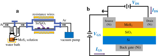
Schematic view of experimental setup and MoS2 nanodisc-based back-gated FET. (a) Schematic view of the experimental setup of CVD. (b) MoS2 FET with 50-nm-thick Ni as contact electrodes together with electrical connections. The channel is the MoS2 nanodiscs, and 280-nm SiO2 serves as gate dielectric. The length and width of the channel are 1.5 and 5 μm, respectively.
Figure 1b is a schematic of a MoS2 back-gated FET. The source and drain electrodes were formed by lithographic patterning, and Ni electrodes were sputtered onto them using magnetron sputtering technology. The MoS2 nanodiscs serve as the channel, whose length and width are 1.5 and 5 μm, respectively. The back gate of the FET was completed by sputtering a 50-nm-thick Ni layer on the back of the Si substrate.
The surface morphology and crystalline structure of the MoS2 discs were analyzed by atomic force microscopy (AFM) and X-ray diffraction (XRD), respectively. The electrical properties of the samples were measured using a Hall Effect Measurement System (HMS-3000, Ecopia, Anyang, South Korea) at room temperature. The electrical properties of the MoS2 nanodisc-based FETs, configured as shown in Figure 1b, were measured using a Keithley 4200 semiconductor characterization system (Cleveland, OH, USA).
Results and discussion
Figure 2a shows the AFM topographic image of the MoS2 discs deposited on the Si substrates. The MoS2 nanodiscs are round and flat, with a diameter of 100 nm and a thickness of around 5 nm, which is equal to the thickness of a few MoS2 layers. The uniform color of the MoS2 nanodiscs in the AFM image, as well as the line profile corresponding to a cross section of the sample, indicating that the nanodiscs all have approximately equal thickness. Figure 2b shows a three-dimensional image of the MoS2 nanodisc film, which further confirms the high quality of the MoS2 nanodisc film.
Figure 2.
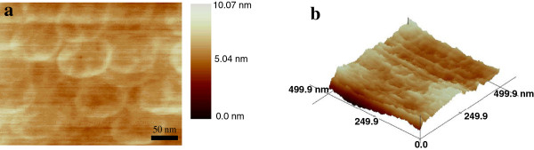
AFM image and three-dimensional distribution of the MoS2 film. (a) An AFM image of the MoS2 nanodisc film deposited on the SiO2/Si substrate. (b) Three-dimensional distribution of the MoS2 nanodiscs.
Figure 3a shows XRD patterns of the obtained MoS2 nanodiscs. Because the intensities of the diffraction peaks differed too widely to be presented in a single plot, the larger plot shows the diffraction peaks in the range of 10° to 60°, while the small insert shows the diffraction peaks that appear between 60° and 70°. Over the whole range of diffraction angles, the MoS2 nanodiscs exhibit eight diffraction peaks, located at 14.7°, 29.5°, 33.1°, 47.8°, 54.6°, 56.4°, 61.7°, and 69.2°. They are assigned, respectively, to the diffraction planes (002), (004), (100), (105), (106), (110), (112), and (108) of MoS2 according to data from the JPDS. The presence of these peaks demonstrates that the obtained MoS2 nanodiscs exhibit a variety of crystal structures. Moreover, the obtained diffraction peaks are rather sharp, which shows that the MoS2 nanodiscs are crystalline over a large area. The peak corresponding to the (108) crystal face is much more intense than the other peaks, indicating that the discs have a strong tendency to adopt the (108) crystal orientation during their growth.
Figure 3.
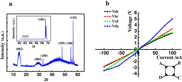
Properties of the MoS2 nanodiscs. (a) XRD pattern of the obtained MoS2 nanodiscs for the diffraction angle in the range of 10° ~ 60°. Inset: the diffraction spectrum of MoS2 nanodiscs for the diffraction angle in the range of 60° ~ 70°. (b) The surface current-voltage curves of the MoS2 nanodiscs. Inset: the layout of four measured points on the MoS2 disc film.
The surface current-voltage (I-V) properties, surface carrier concentration and mobility of the obtained MoS2 nanodiscs are very sensitive to the quality of the film. Figure 3b shows the surface I-V properties of the MoS2 nanodisc film. The inset shows the layout of the four measurement points on the MoS2 nanodisc film. The I-V curves measured between any two points show a perfect linear dependence, which indicates that the deposited MoS2 nanodiscs have good conductivity. The measured carrier concentration of the MoS2 discs is about 3.412 × 106 cm−2, and their electron mobility is as high as 6.42 × 102 cm2/Vs. This mobility value is higher than previously reported values (2 to 3 × 102 cm2/Vs) for single and multilayer MoS2[19,28]. This significant increase of room-temperature mobility value in our MoS2 may result from the MoS2 nanodisc structure. The mobility of SL MoS2 is generally smaller than bulk MoS2 because of the larger phonon scattering [29]. However, FL MoS2 exhibits fewer dangling bonds and defect states than does SL MoS2, significantly decreasing the phonon scattering. The lattice scattering in the two-dimensional (2D) nanodiscs should be even lower, due to their surface roughness and boundaries. The above findings clearly demonstrate that the MoS2 nanodiscs fabricated via CVD have uniform morphologies, structures, and electrical properties.
The electrical properties of the MoS2 nanodisc-based back-gated FETs, with Ni as the source, drain, and back gate contacts were next investigated at room temperature. Figure 4a shows the relationship between the gate current (IGS) and the gate voltage (VGS) of the transistor at a drain voltage (VDS) of 5 V. The current through the device increases exponentially with the applied positive voltage, and tends to be almost zero under the revised voltage, showing that the MoS2 transistor is a good rectifier.
Figure 4.
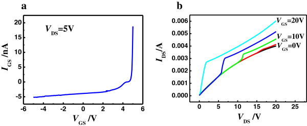
The current–voltage behavior of back-gated MoS2 transistor. (a) Gate current IGS versus gate voltage VGS behavior of back-gated MoS2 transistor at room temperature for the drain voltage VDS value of 5 V. (b) Output characteristics of back-gated MoS2 transistors at room temperature for VGS values of 0, 5, 10, 15, and 20 V.
Figure 4b displays the output characteristics (drain current IDS versus drain voltage VDS) of back-gated MoS2 transistors at room temperature for VGS = 0, 5, 10, 15, and 20 V. For small VGS, the current IDS shows an exponential dependence on VDS at low VDS values, which results from the presence of a sizable Schottky barrier at the Ni-MoS2 interface [12]. Then, for larger values of VGS, the relation between IDS and VDS becomes linear as VDS increases, which is consistent with the previously reported findings [12]. The barrier height at larger VGS is lower that has been previously demonstrated in greater detail [12,30,31]. Thus, the channel can give rise to thermally assisted tunneling, which is responsible for the linear relationship between IDS and VDS. Finally, when VDS increases above a certain value, the current IDS becomes saturated, achieving the output properties of a traditional FET.
Figure 5a shows the transfer characteristics (IDS/VGS) of the back-gated MoS2 transistor at room temperature for VDS = 1 V. It is clear that the gate leakage of the FET is negligible and the on/off current ratio can be up to 1.9 × 10⁵, larger than that in the WSe2-based FETs at low temperature [32], which demonstrates that the MoS2 transistor can be easily modulated by the back gate. Moreover, the Fermi level of Ni is close to the conduction band edge of MoS2, consistent with earlier reports [7,12], which makes MoS2 transistors exhibit mostly n-type behavior. Figure 5b shows the variation of the device transconductance gm (gm = dIDS/dVGS) with VGS at VDS = 1 V. The extracted maximum gm is about 27μS (5.4 μS/μm) within the entire range of VGS, better than previously reported values [7,12]. The field effect mobility μ also can be obtained based on the conventional dependence of μ = gm [L/(W · COX · VDS)] at VDS = 1 V, where gm is the maximum value of gm, and L and W are the length and width of the channel, and COX = 1.1 × 10⁻⁴ F/m2 is the gate capacitance per unit area [33]. COX is equal to ϵOX/dOX, where ϵOX is the dielectric constant and dOX is the thickness of the gate dielectric. Using this relationship, the field effect mobility μ is as high as 368 cm2/Vs, comparable to that of single and multilayer MoS2 FETs [7,10,12,26,34]. Note that the field effect mobility is lower than the electron mobility of the MoS2 nanodiscs, which is likely due to the presence of scattering and defect states.
Figure 5.
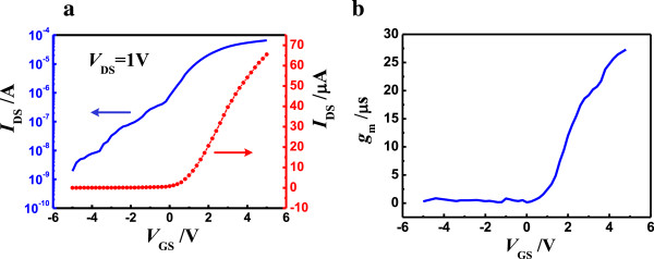
Transfer characteristics of back-gated MoS2 transistor (a) and device transconductance versus gate voltage (b). (a) Transfer characteristics of MoS2 transistor at room temperature for the VDS value of 1 V on logarithmic (left axis) and linear scales (right axis). (b) Device transconductance gm (defined as gm = dIDS/dVGS) versus gate voltage VGS at VDS = 1 V.
Conclusions
Using CVD, we have fabricated uniform MoS2 nanodiscs, organized into thin films with large area and having good electrical properties. The nanodiscs were incorporated into high-performance back-gated field effect transistors with Ni as contact electrodes. The transistors have good output characteristics and exhibit typical n-type behavior, with a maximum transconductance of approximately 27 μS (5.4 μS/μm), an on/off current ratio of up to 1.9 × 10⁵ and a mobility as high as 368 cm2/Vs, comparable to that of FETs based on single and multilayer MoS2. These promising values along with the very good electrical characteristics, MoS2 transistors will be the attractive candidates for future low-power applications.
Competing interests
The authors declare that they have no competing interests.
Authors’ contributions
WG participated in the fabrication of MoS2 nanodiscs on the substrate, measured the electrical properties of the transistor, and wrote the manuscript. JS fabricated the drain, source, and gate of the transistor and participated in the analysis of the results of the transistor. XM designed the structure of the transistor and analyzed the results. All authors read and approved the final manuscript.
Authors’ information
WG is a graduate student major in fabrication of new semiconductor nanometer materials. JS is a lecturer and PhD-degree holder specializing in semiconductor devices. XM is a professor and PhD-degree holder specializing in semiconductor materials and devices, especially expert in nanoscaled optical-electronic materials and optoelectronic devices.
Contributor Information
Weixia Gu, Email: guweixia0920@163.com.
Jiaoyan Shen, Email: shenjiaoyan@hotmail.com.
Xiying Ma, Email: maxy@mail.usts.edu.cn.
Acknowledgements
This work was supported in part by the National Natural Science Foundation of China (no. 60976071) and the Innovation Program for Postgraduate of Suzhou University of Science and Technology (No. SKCX13S_053).
References
- Novoselov KS, Geim AK, Morozov SV, Jiang D, Katsnelson MI, Grigorieva IV, Dubonos SV, Firsov AA. Two-dimensional gas of massless Dirac fermions in graphene. Nature. 2005;9:197. doi: 10.1038/nature04233. [DOI] [PubMed] [Google Scholar]
- Kam KK, Parkinson BA. Detailed photocurrent spectroscopy of the semiconducting group VIB transition metal dichalcogenides. J Phys Chem. 1982;9:463. doi: 10.1021/j100393a010. [DOI] [Google Scholar]
- Lebègue S, Eriksson O. Electronic structure of two-dimensional crystals from ab initio theory. Phys Rev B. 2009;9:115409. [Google Scholar]
- Splendiani A, Sun L, Zhang Y, Li T, Kim J, Chim CY, Galli G, Wang F. Emerging photoluminescence in monolayer MoS2. Nano Lett. 2010;9:1271. doi: 10.1021/nl903868w. [DOI] [PubMed] [Google Scholar]
- Mak KF, Lee C, Hone J, Shan J, Heinz TF. Atomically thin MoS2: a new direct-gap semiconductor. Phys Rev Lett. 2010;9:136805. doi: 10.1103/PhysRevLett.105.136805. [DOI] [PubMed] [Google Scholar]
- Kuc A, Zibouche N, Heine T. Influence of quantum confinement on the electronic structure of the transition metal sulfide TS2. Phys Rev B. 2011;9:245213. [Google Scholar]
- Radisavljevic B, Radenovic A, Brivio J, Giacometti V, Kis A. Single-layer MoS2 transistors. Nat Nanotechnol. 2011;9:147. doi: 10.1038/nnano.2010.279. [DOI] [PubMed] [Google Scholar]
- Radisavljevic B, Whitwick MB, Kis A. Integrated circuits and logic operations based on single-layer MoS2. ACS Nano. 2011;9:9934. doi: 10.1021/nn203715c. [DOI] [PubMed] [Google Scholar]
- Liu H, Ye PD. MoS2 dual-gate MOSFET with atomic-layer-deposited Al2O3 as top-gate dielectric. IEEE Trans Electron Devices. 2012;9:546. [Google Scholar]
- Qiu H, Pan L, Yao Z, Li J, Shi Y, Wang X. Electrical characterization of back-gated bi-layer MoS2 field-effect transistors and the effect of ambient on their performances. Appl Phys Lett. 2012;9:123104. doi: 10.1063/1.3696045. [DOI] [Google Scholar]
- Lee K, Kim HY, Lotya M, Coleman JN, Kim GT, Duesberg GS. Electrical characteristics of molybdenum disulfide flakes produced by liquid exfoliation. Adv Mater. 2011;9:4178. doi: 10.1002/adma.201101013. [DOI] [PubMed] [Google Scholar]
- Das S, Chen HY, Penumatcha AV, Appenzeller J. High performance multilayer MoS2 transistors with scandium contacts. Nano Lett. 2013;9:100. doi: 10.1021/nl303583v. [DOI] [PubMed] [Google Scholar]
- Yoon Y, Ganapathi K, Salahuddin S. How good can monolayer MoS2 transistors be? Nano Lett. 2011;9:3768. doi: 10.1021/nl2018178. [DOI] [PubMed] [Google Scholar]
- Takahashi T, Takenobu T, Takeya J, Iwasa Y. Ambipolar light-emitting transistors of a tetracene single crystal. Adv Funct Mater. 2007;9:1623. doi: 10.1002/adfm.200700046. [DOI] [Google Scholar]
- Yin Z, Li H, Li H, Jiang L, Shi Y, Sun Y, Lu G, Zhang Q, Chen X, Zhang H. Single-layer MoS2 phototransistors. ACS Nano. 2012;9:74. doi: 10.1021/nn2024557. [DOI] [PubMed] [Google Scholar]
- Gourmelon E, Lignier O, Hadouda H, Couturier G, Bernède JC, Tedd J, Pouzet J, Salardenne J. MS2 (M = W, Mo) Photosensitive thin films for solar cells. Sol Energy Mater Sol Cells. 1997;9:115. doi: 10.1016/S0927-0248(96)00096-7. [DOI] [Google Scholar]
- Zong X, Yan H, Wu G, Ma G, Wen F, Wang L, Li C. Enhancement of photocatalytic H2 evolution on CdS by loading MoS2 as cocatalyst under visible light irradiation. J Am Chem Soc. 2008;9:7176. doi: 10.1021/ja8007825. [DOI] [PubMed] [Google Scholar]
- Novoselov KS, Geim AK, Morozov SV, Jiang D, Zhang Y, Dubonos SV, Grigorieva IV, Firsov AA. Electric field effect in atomically thin carbon films. Science. 2004;9:666. doi: 10.1126/science.1102896. [DOI] [PubMed] [Google Scholar]
- Novoselov KS, Jiang D, Schedin F, Booth TJ, Khotkevich VV, Morozov SV, Geim AK. Two-dimensional atomic crystals. Proc Natl Acad Sci USA. 2005;9:10451. doi: 10.1073/pnas.0502848102. [DOI] [PMC free article] [PubMed] [Google Scholar]
- Joensen P, Frindt RF, Morrison SR. Single-layer MoS2. Mater Res Bull. 1986;9:457. doi: 10.1016/0025-5408(86)90011-5. [DOI] [Google Scholar]
- Schumacher A, Scandella L, Kruse N, Prins R. Single-layer MoS2 on mica: studies by means of scanning force microscopy. Surf Sci Lett. 1993;9:L595. [Google Scholar]
- Coleman JN, Lotya M, O'Neill A, Bergin SD, King PJ, Khan U, Young K, Gaucher A, De S, Smith RJ, Shvets IV, Arora SK, Stanton G, Kim HY, Lee K, Kim GT, Duesberg GS, Hallam T, Boland JJ, Wang JJ, Donegan JF, Grunlan JC, Moriarty G, Shmeliov A, Nicholls RJ, Perkins JM, Grieveson EM, Theuwissen K, McComb DW, Nellist PD. et al. Two-dimensional nanosheets produced by liquid exfoliation of layered materials. Science. 2011;9:568. doi: 10.1126/science.1194975. [DOI] [PubMed] [Google Scholar]
- Lauritsen JV, Kibsgaard J, Helveg S, Topsoe H, Clausen BS, Lagsgaard E, Besenbacher F. Size-dependent structure of MoS2 nanocrystals. Nat Nanotechnol. 2007;9:53. doi: 10.1038/nnano.2006.171. [DOI] [PubMed] [Google Scholar]
- Li Q, Newberg JT, Walter JC, Hemminger JC, Penner RM. Polycrystalline molybdenum disulfide (2H-MoS2) nano- and microribbens by electrochemicl/chemical synthesis. Nano Lett. 2004;9:277. doi: 10.1021/nl035011f. [DOI] [Google Scholar]
- Balendhran S, Ou JZ, Bhaskaran M, Sriram S, Ippolito S, Vasic Z, Kats E, Bhargava S, Zhuiykov S, Kalantar-zadeh K. Atomically thin layers of MoS2 via a two step thermal evaporation − exfoliation method. Nanoscale. 2012;9:461. doi: 10.1039/c1nr10803d. [DOI] [PubMed] [Google Scholar]
- Liu KK, Zhang W, Lee YH, Lin YC, Chang MT, Su CY, Chang CS, Li H, Shi Y, Zhang H, Lai CS, Li LJ. Growth of large-area and highly crystalline MoS2 thin layers on insulating substrates. Nano Lett. 2012;9:1538. doi: 10.1021/nl2043612. [DOI] [PubMed] [Google Scholar]
- Zhan Y, Liu Z, Najmaei S, Ajayan PM, Lou J. Large-area vapor-phase growth and characterization of MoS2 atomic layers on a SiO2 substrate. Small. 2012;9:966. doi: 10.1002/smll.201102654. [DOI] [PubMed] [Google Scholar]
- Ayari A, Cobas E, Ogundadegbe O, Fuhrer MS. Realization and electrical characterization of ultrathin crystals of layered transition-metal dichalcogenides. J Appl Phys. 2007;9:014507. doi: 10.1063/1.2407388. [DOI] [Google Scholar]
- Pradhan NR, Rhodes D, Zhang Q, Talapatra S, Terrones M, Ajayan PM, Balicas L. Intrinsic carrier mobility of multi-layered MoS2 field-effect transistors on SiO2. Appl Phys Lett. 2013;9:123105. doi: 10.1063/1.4799172. [DOI] [Google Scholar]
- Appenzeller J, Knoch J, Bjork MT, Riel H, Schmid H, Riess W. Towards nanowire electronics. IEEE Trans Electron Devices. 2008;9:2827. [Google Scholar]
- Heinze S, Tersoff J, Martel R, Derycke V, Appenzeller J, Avouris P. Carbon nanotubes as Schottky barrier transistors. Phys Rev Lett. 2002;9:106801. doi: 10.1103/PhysRevLett.89.106801. [DOI] [PubMed] [Google Scholar]
- Podzorov V, Gershenson ME, Kloc C, Zeis R, Bucher E. High-mobility field-effect transistors based on transition metal dichalcogenides. Appl Phys Lett. 2004;9:3301. doi: 10.1063/1.1723695. [DOI] [Google Scholar]
- Lee CW, Weng CH, Wei L, Chen Y, Chan-Park MB, Tsai CH, Leou KC, Poa CHP, Wang J, Li LJ. Toward high-performance solution-processed carbon nanotube network transistors by removing nanotube bundles. J Phys Chem C. 2008;9:12089. doi: 10.1021/jp805434d. [DOI] [Google Scholar]
- Wang H, Yu L, Lee YH, Shi Y, Hsu A, Chin ML, Li LJ, Dubey M, Kong J, Palacios T. Integrated circuits based on bilayer MoS2 transistors. Nano Lett. 2012;9:4674. doi: 10.1021/nl302015v. [DOI] [PubMed] [Google Scholar]