Abstract
We present an adaptive reconfigurable active voltage doubler (VD)/rectifier (REC) (VD/REC) in standard CMOS, which can adaptively change its topology to either a VD or a REC by sensing the output voltage, leading to more robust inductive power transmission over an extended range. Both active VD and REC modes provide much lower dropout voltage and far better power conversion efficiency (PCE) compared to their passive counterparts by adopting offset-controlled high-speed comparators that drive the rectifying switches at proper times in the high-frequency band. We have fabricated the active VD/REC in a 0.5-µm 3-metal 2-poly CMOS process, occupying 0.585 mm2 of chip area. In an exemplar setup, VD/REC extended the power transmission range by 33% (from 6 to 8 cm) in relative coil distance and 41.5% (from 53° to 75°) in relative coil orientation compared to using the REC alone. While providing 3.1-V dc output across a 500-Ω load from 2.15- (VD) and 3.7-V (REC) peak ac inputs at 13.56 MHz, VD/REC achieved measured PCEs of 70% and 77%, respectively.
Index Terms: Active rectifier (REC), active voltage doubler (VD), adaptive control, high-speed comparators, implantable microelectronic devices (IMDs), inductive power transmission, near field
I. Introduction
Modern implantable microelectronic devices (IMDs) require high power efficiency and performance to enable more efficacious therapies, particularly in neuroprostheses such as retinal and cochlear implants [1]. Inductive wireless power transmission across the skin is currently the only viable solution for providing sufficient power to such IMDs without imposing size and power constraints of implanted batteries [2]. On the downside, unlike batteries that provide a stable power source, unexpected variations in the coils’ mutual coupling M, which mainly result from coil misalignments, can lead to wide variations in the received voltage across the secondary to the extent that the input voltage may not be sufficient to supply the IMD [3]. Hence, there is a need to improve the robustness of the inductive power links without sacrificing efficiency to allow the IMDs to operate over a wider range of received input voltages. There are also other applications such as wireless sensors, radio frequency identification, and near-field communication, in which extending the range of loosely coupled inductive links is highly desired [4].
Active rectifiers (RECs) and voltage doublers (VDs) using synchronous switches have been widely used to convert ac input signals to dc outputs for inductively powered applications [5]–[8]. RECs require peak inputs higher than the desired outputs, which may be temporarily limited by the weak coupling of the inductive links. On the contrary, active VDs are capable of generating higher output voltages, but their power conversion efficiencies (PCEs) are generally lower than those of active RECs with similar size. In order to address such limitations, we have proposed a power-efficient reconfigurable active VD/REC for robust wireless power transmission through inductive links over an extended range. Both VD and REC modes are integrated into a single structure, employing low dropout active synchronous switches, leading to high PCE. Moreover, by adding an output-voltage-sensing circuit, VD/REC can automatically change its operating mode to either VD or REC depending on which one is a better choice for generating the desired output voltage to accommodate with a wider range of mutual coil arrangements.
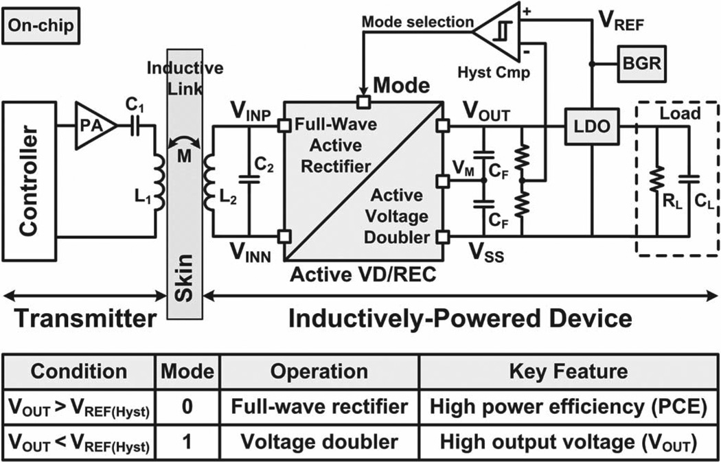
Fig. 1 shows the block diagram of a wireless power transmission link that includes the proposed VD/REC. A power amplifier (PA) drives the primary coil L1 at the designated carrier frequency (fc = 13.56 MHz), which improves the coils’ quality factors (Q) and increases the overall power transmission efficiency, while maintaining the sizes of LC components small for implantable applications [3]. A coupled signal across the secondary L2 creates an ac voltage VIN (= VINP − VINN) across L2C2 which is tuned at fc. VD/REC, which follows the L2C2 tank, converts VIN to an automatically adjusted dc voltage VOUT for supplying the load after regulation. If VIN falls below a certain level, which is determined by comparing a portion of VOUT with a reference voltage VREF using a hysteresis comparator, then Mode = 1 and VD/REC operates in VD mode. Since the VD can generate the desired VOUT with much lower VIN than the REC, VD/REC can still provide sufficient VOUT to the load even with decreased VIN. On the other hand, if VIN increases above VREF + hysteresis window, then Mode = 0 and VD/REC will operate in the REC mode, which can achieve higher PCE than the VD mode while generating the desired VOUT.
Fig. 1.
Block diagram of an inductively powered device with emphasis on the wireless power transmission through the proposed active VD/REC converter.
The rest of this brief, which is an extended version of [9], is organized as follows. Section II describes the concept and implementation of active VD/REC. Section III presents the circuit details and design considerations including the offset-controlled high-speed comparators, start-up circuit, and mode selection circuit. The measurement results are in Section IV, followed by the conclusion in Section V.
II. Active VD/REC Architecture
A. Concept of the Active VD/REC
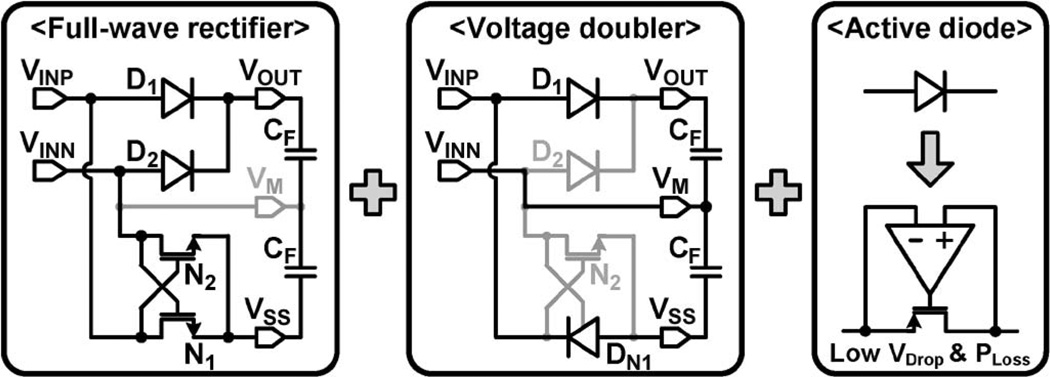
The concept of active VD/REC starts from combining two separate ac-to-dc converters, a REC and a VD, into a single structure in which the operating mode, REC or VD, is selected by an external mode selection signal. Fig. 2 shows the conceptual diagram of the active VD/REC converter which consists of a full-wave REC and a VD with active diodes. The full-wave REC requires two diodes D1 and D2 and a cross-coupled NMOS pair N1 and N2. Either the D1−N2 path or the D2−N1 path is activated depending on the amplitudes of VINP and VINN to transfer the input power to the output filtering capacitors CF/2. The VD requires only two diodes D1 and DN1, charging one CF per half cycle depending on the polarity and amplitude of VIN (= VINP − VINN). Therefore, VOUT becomes almost doubled compared to the peak voltage of VIN. In order for VD/REC to include both structures, D1 is shared, and D2 and N2 have enable functions to turn them on/off in the REC and VD modes, respectively. N1 operates as part of a cross-coupled pair in the REC mode, while it is reconfigured as an NMOS diode DN1 in the VD mode. VINN and VM are also shorted through a switch N3 in the VD mode. VD/REC utilizes active diodes D1, D2, and DN1, in which rectifying pass transistors are driven by fast comparators to operate as switches in the deep triode region with low dropout voltages. Therefore, these active diodes dissipate less power compared to passive diodes, leading to higher PCE in both operating modes.
Fig. 2.
Conceptual diagram of the active VD/REC converter in which a full-wave REC and a VD are combined using active diodes.
B. Implementation of the Active VD/REC
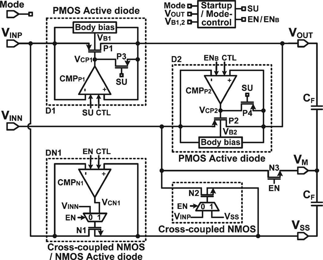
Fig. 3 shows a simplified schematic diagram of the VD/REC, consisting of PMOS and NMOS active diodes D1, D2, and DN1, in which pass transistors P1, P2, and N1 are driven by high-speed comparators CMPP1, CMPP2, and CMPN1, respectively, to minimize ac–dc dropout voltage and power loss. Mode signals EN and ENB, which are derived from the mode control circuit, can reconfigure the VD/REC topology for rectification or doubling functions, as shown in Fig. 2. In the REC mode (EN = 0 and ENB = 1), the gates of N1 and N2 are connected to VINN and VINP, respectively, resulting in a cross-coupled NMOS pair with positive feedback, while CMPN1 is deactivated. Both PMOS active diodes are utilized in this mode, alternating every half cycle to transfer input power to the load. For example, when VINP > VINN, N2 turns on, while N1 turns off. Then, when VINP > VOUT, the CMPP1 output goes low, turning P1 on with a low dropout voltage. The input current in this case flows from VINP through P1 to charge CF/2 and returns back to VINN through N2. In the VD mode (EN = 1 and ENB = 0), P2 and N2 are always off, and CMPP2 is deactivated. Only P1 and N1 operate as active diodes, while N3 strongly connects VINN to VM for charging the filtering capacitors CF, one per half cycle, to almost double VOUT in reference to VSS.
Fig. 3.
Schematic diagram of the proposed VD/REC employing active diodes to achieve lower dropout voltage and higher PCE for both REC and VD modes.
Since the comparators in active diodes are supplied from VOUT, which is initially at 0 V, self-start-up capability is a feature necessary in active VD/REC. The start-up circuit in Fig. 3 monitors VOUT and sets SU = EN = ENB = 0 when VOUT is too low. At start-up, N1 and N2 are cross-coupled through multiplexers (MUXs), and P1 and P2 are diode connected through P3 and P4, respectively, forming a passive REC, which charges VOUT regardless of the comparators’ status up to the point where VOUT reaches a desired level. Then, SU toggles to enable VD/REC to operate normally. PMOS body terminals VB1 and VB2 are always connected to the highest potential among VINP,N and VOUT via their body bias circuits.
III. Circuit Details and Design Considerations
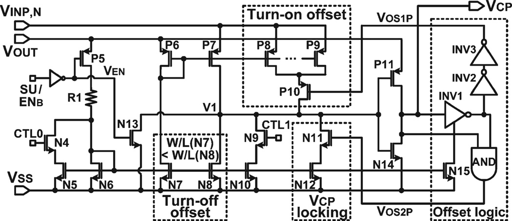
In order to drive large pass transistors at 13.56 MHz, comparators need to have short turn-on/turn-off delays, which may otherwise reduce the PCE by either decreasing the input power delivered to the load or allowing instantaneous reverse current back from CF. We have used high-speed comparators with built-in offset-control functions to expedite VOUT transitions by compensating for both turn-on and turn-off delays [10]. Fig. 4 shows the schematic diagram of the high-speed comparator CMPP, which is equipped with three offset-control functions: turn-on, turn-off, and output-locking offsets. In Fig. 4, P6, P7, N7, N8, P11, and N14 form a common-gate comparator, in which input voltages (VOUT and VINP,N) are applied to the sources of P6 and P7. The turn-on offset block, consisting of P8 and P9 current sources and P10 control switch, injects additional offset current to force V1 to increase earlier, leading to fast turn-on of P1,2 in Fig. 3. The offset-control signal VOS1P deactivates P10 just after turning P1,2 on and activates it again after the current-starved inverter (INV1 and N15) delay, which does not need to be accurate as long as it is shorter than one carrier cycle. The turn-off offset function utilizes the size mismatch between N7 and N8, where the larger N8 pulls additional current from the V1 node, forcing V1 to start dropping earlier to turn P1,2 off at the right time. After the comparator output VCP goes high and turns P1,2 off, N11 is activated by VOS2P for the current-starved inverter delay time to keep V1 low and prevent VCP from bouncing due to VINP,N variations. CMPN has a similar but symmetrical structure. In addition, 4-bit off-chip digital control signals, CTL0:1 for CMPP and CTL2:3 for CMPN, are utilized to adjust the switching times of VD/REC against process variations.
Fig. 4.
Schematic diagram showing three built-in offset-control functions, which are turn-on, turn-off, and output-locking offsets, in our high-speed comparator CMPP [10].
In the start-up circuit in Fig. 5(a), when VOUT is very low, P12 turns off and SU goes low, resulting in P1 and P2 in Fig. 3 to stay diode connected through P3 and P4, respectively. During the same period, both EN and ENB of the mode control circuit in Fig. 5(b) become low, so all comparators are in the sleep mode while N1 and N2 are cross-coupled through MUXs, leading the VD/REC to operate as a passive REC. With SU = ENB = 0, N13 in Fig. 4 forces VCP1,2 to be high, further supporting P1 and P2 to be diode connected. When VOUT > VTh(N16) + VTh(P12), SU toggles high, turning P3 and P4 off, releasing the comparator outputs, and allowing P1 and P2 to operate as switches [10]. The mode control circuit consists of two pairs of level shifters and logic gates, one of which is shown in Fig. 5(b), to level shift the mode signal to either VB1 or VB2 (in Fig. 3) for creating the EN and ENB signals, which control various switches at proper voltage levels. In Fig. 5(c), the body bias circuit automatically connects VB1 and VB2 to max(VINP, VOUT) and max(VINN, VOUT), respectively, through P17 and P18 [6].
Fig. 5.
Schematic diagrams of the (a) start-up circuit, (b) mode control circuit, and (c) body bias circuit.
IV. Measurement Results
A. Chip Micrograph and Measured Waveforms
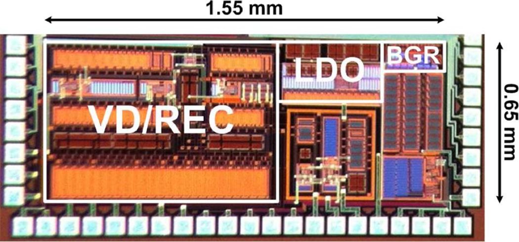
VD/REC was fabricated in the ON Semiconductor 0.5-µm 3M2P n-well standard CMOS process, occupying 0.585 mm2. Fig. 6 shows the chip micrograph and floor plan of the VD/REC, low dropout regulator (LDO), and bandgap reference (BGR). The sizes of the main rectifying transistors are as follows: WP1,2 = 3300 µm, WN1,2 = 1800 µm, and WN3 = 12 000 µm with a minimum length of L = 0.6 µm.
Fig. 6.
Fabricated chip micrograph of the VD/REC in the ON Semiconductor 0.5-µm standard CMOS process, occupying an area of 0.585 mm2.
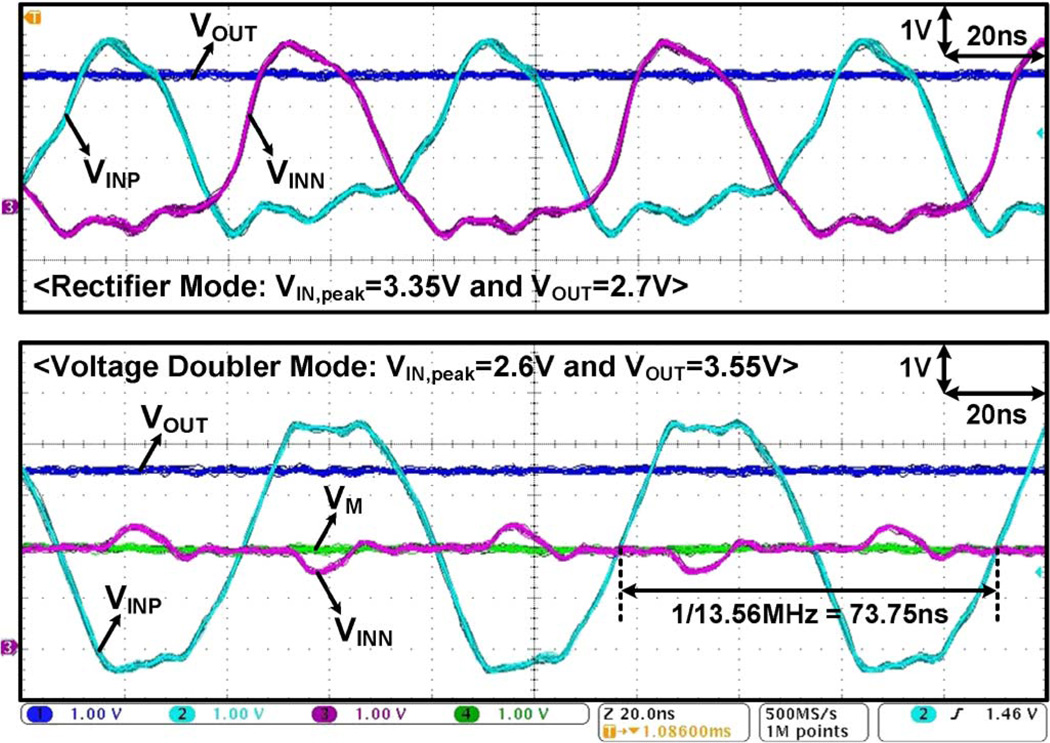
Fig. 7 shows the measured input/output waveforms in the REC and VD modes with RL‖CF/2 = 1 kΩ‖0.5 µF (no regulator) at fc = 13.56 MHz. The same supply voltage was applied to the PA on the primary side to verify the VOUT difference between the REC and VD modes. In the REC mode (Mode = 0), VINP and VINN charge VOUT alternatively, resulting in VIN,peak(REC) = 3.35 V and VOUT = 2.7 V. In the VD mode (Mode = 1), VINN is shorted via N3 to VM, the middle voltage of VOUT, and VINP goes well above VIN,peak(REC) to achieve VOUT = 3.55 V with VIN,peak(VD) = 2.6 V. Large instantaneous input currents flow into the VD/REC during the conduction period, inducing the voltage drop across N3, which is VINN − VM. VIN,peak(VD) is less than VIN,peak(REC) because of a reduction in the inductive link Q factor due to higher input and output currents in the VD mode.
Fig. 7.
Measured input/output voltage waveforms in the (top) REC and (bottom) VD modes when RL‖CF/2 = 1 kΩ‖0.5 µF (no regulator) and fc = 13.56 MHz.
B. Power Transmission Range and PCE Measurements
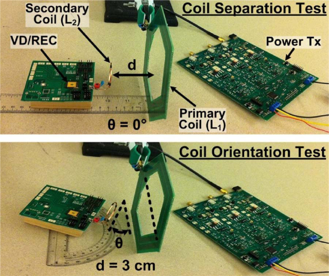
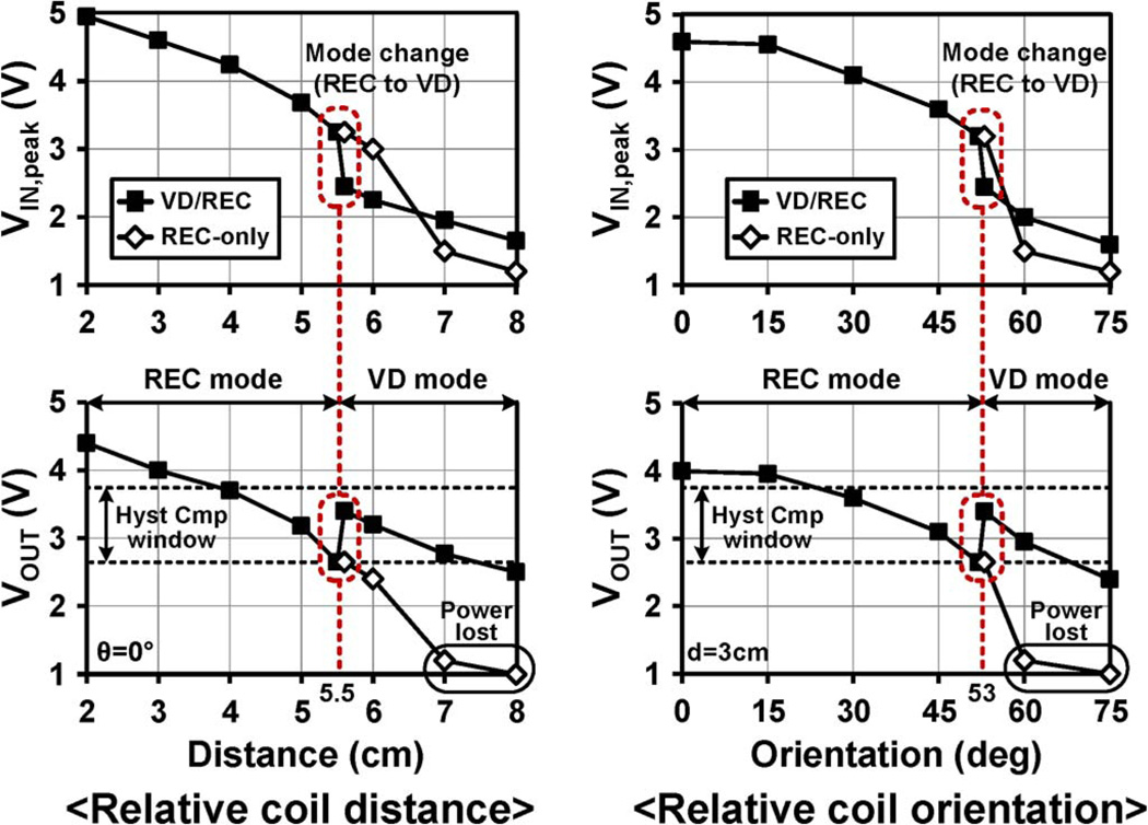
In order to verify the benefits of using the VD/REC over a REC, we have measured VIN,peak and VOUT while sweeping the relative distance (d) and orientation (θ) between a pair of coupled coils L1 and L2, as shown in Fig. 8. In this test setup, whose specifications are shown in Table II, a class-C PA on the transmitter side (Tx) drives the inductive link to induce a 13.56-MHz sinusoidal signal across the VD/REC. Fig. 9 shows the measured VIN,peak and VOUT versus d and θ and demonstrates how using the VD/REC extends the inductive link power transmission range in terms of the coils’ relative distance and angular misalignment compared to REC only. The hysteresis window of the off-chip comparator was set to 2.6–3.7 V and indicated on the graphs as horizontal dashed lines. In the d-sweep test, the VD/REC operates in the REC mode when d is small. VOUT drops as d increases, and when d > 5.5 cm, VD/REC switches to the VD mode, increasing VOUT by 0.8 V (30.8%). As a result, VD/REC maintains sufficient VOUT > 2.5 V for coil separations up to d = 8cm, compared to the REC only, which fails at d > 6 cm (a 33% improvement). Similarly, VD/REC improved the inductive link tolerance to coil rotations by extending the range from θ = 53° (REC only) to θ = 75° (VD/REC) at d = 3 cm (a 41.5% improvement).
Fig. 8.
Test setup for measuring the PCE and input/output voltages of the active VD/REC ac-to-dc converter when sweeping the relative coil (top) distance and (bottom) orientation.
TABLE II.
Additional Active VD/REC Measurement Setup Specifications
| Nominal output power | 6 ~ 37 mW |
| Output filtering capacitor (CF) | 1 µF |
| Output ripple (RL = 0.5 kΩ) | 50 mVpp |
| Bandgap reference voltage (VREF) | 1.187 V |
| Primary coil diameter / inductance (L1) | 16.8 cm / 0.88 µH |
| Secondary coil diameter / inductance (L2) | 3.0 cm / 0.41 µH |
| Total area of the VD/REC | 0.585 mm2 |
Fig. 9.
Measured input and output voltages while sweeping the coil relative distance (d) and orientation (θ) in Fig. 8, which clarify that using VD/REC extends the inductive link power transmission range.
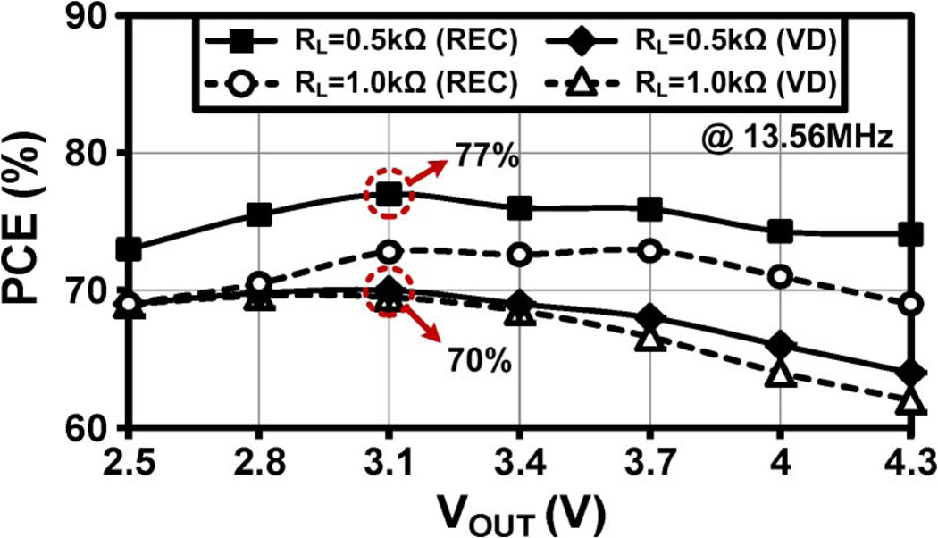
To consider the practical conditions in which the output voltage of the VD/REC varies due to coil misalignments as well as loading changes, we measured the PCE while sweeping VOUT by adjusting the Tx output power delivered to the primary coil L1. The PCE of VD/REC can be defined as the delivered power to the load over the input power from the L2C2 tank. Fig. 10 shows the measured PCE versus VOUT in both REC and VD modes with RL = 0.5 and 1 kΩ at fc = 13.56 MHz. The highest PCEs of the REC and VD modes were 77% and 70%, respectively, at VOUT = 3.1 V with RL = 0.5 kΩ. The PCE drops for VOUT > 3.7 V and VOUT < 2.8 V are mainly due to the pass transistor sizing and comparator offsets which were designed for VOUT = 2.8−3.7 V. The VD/REC still operates properly against VOUT variations with PCE > 74% within VOUT = 2.6−4.3 V in the REC mode and PCE > 68.5% within VOUT = 2.5−3.7 V in the VD mode for RL = 0.5 kΩ. The VOUT range is determined based on the hysteresis comparator window of 2.6–3.7 V. Table I benchmarks the proposed active VD/REC against several recently reported RECs and VDs. Table II provides a few additional specifications of the VD/REC and the inductive link used in our measurements.
Fig. 10.
Measured PCE versus VOUT with RL = 0.5 and 1 kΩ at fc = 13.56 MHz, leading to the highest PCEs of 77% and 70% in the REC and VD modes, respectively.
TABLE I.
REC and VD Benchmarking
| Publication | [5] | [6] | [7] | [8] | This work | ||
|---|---|---|---|---|---|---|---|
| Technology | 0.18µm | 0.5µm | 0.18µm | 0.8µm | 0.5µm CMOS | ||
| Structure | REC | REC | Multiplier | VD | Active VD/REC | ||
| VD | REC | ||||||
| VIN, peak (V) | 1.25 | 3.8 | 0.8 | 11.1 | 2.15 | 3.7 | |
| VOUT (V) | 0.96 | 3.12 | 1.8 | 20 | 3.1 | 3.1 | |
| VCE (%)* | 76.8 | 82.1 | 56.3 | 90.1 | 72.1 | 83.8 | |
| RL (kΩ) | 2 | 0.5 | 270 | 20 | 0.5 | ||
| fc (MHz) | 10 | 13.56 | 13.56 | 13.56 | 13.56 | ||
| Area (mm2) | 0.86 | 0.18 | 0.83 | N/A | 0.585 | ||
| PCE (%) | Sim. | N/A | 87 | N/A | 90.5 | 75 | 81 |
| Meas. | 76 | 80.2 | 54.9 | N/A | 70 | 77 | |
Voltage conversion efficiency (VCE) = VOUT/(VIN, peak × multiplication factor)
C. In Vitro Experiments
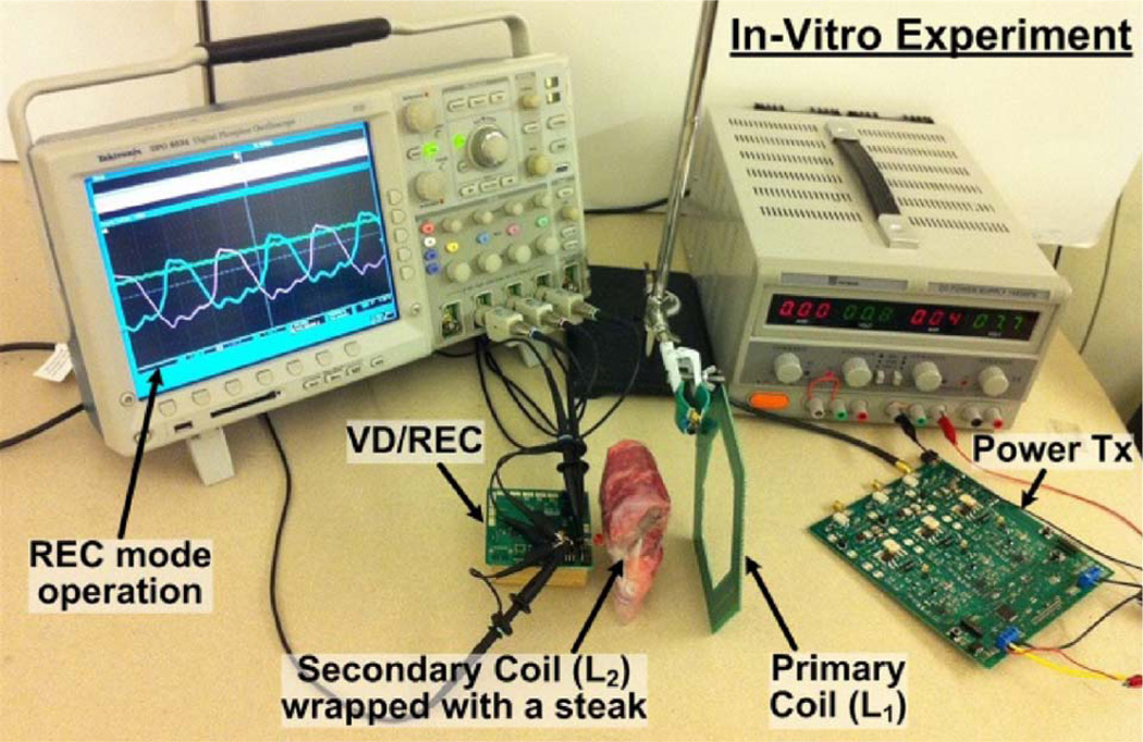
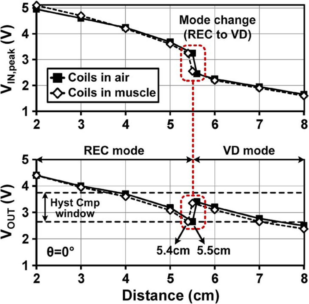
Inductively powered IMDs that employ the active VD/REC converter need to be hermetically sealed in biocompatible materials and placed in a conductive tissue environment with high permittivity, which can affect not only the secondary coil characteristics but also the VD/REC performance [11]. In order to emulate the implant environment, we conducted in vitro experiments with the test setup in Fig. 11, in which the secondary coil (L2) was wrapped in a piece of steak (bovine sirloin). Fig. 12 shows the measured VIN,peak and VOUT while sweeping the coils’ relative distance (d) in the air (Fig. 8) and muscle (Fig. 11) environments. The muscle environment leads to a small reduction in both VIN,peak and VOUT compared to the air environment when d is increased. This is because wrapping L2 with a piece of steak increases its parasitic capacitance and resistance, leading the quality factor (Q) of the secondary coil to decrease and the power loss in its parasitic resistance to increase. However, these curves show that using the VD/REC still extends the inductive link power transmission range in both environments to d > 8 cm.
Fig. 11.
Test setup for in vitro experiments that resemble an IMD environment with the secondary coil L2 wrapped in a piece of steak.
Fig. 12.
Measured input and output voltages while sweeping the coils’ relative distance in the air (Fig. 8) and muscle (Fig. 11) environments.
V. Conclusion
Inductive power transmission across the skin is considered the most promising solution for providing sufficient power to IMDs without suffering from size and power constraints of implanted batteries. However, large variations in the received voltage across the secondary coil, which mainly result from coil misalignments or loading variations, can lead to insufficient supply voltage for the IMD. In order to overcome this limitation, we have developed a power-efficient reconfigurable active VD/REC, which can automatically change its operating mode to operate as either a VD or a REC, depending on which one is more suitable for generating the desired output voltage at the highest possible PCE, enabling robust power transmission across the inductive link over an extended range. The presented VD/REC has been equipped with active diodes, in which high-speed comparators synchronously control MOS switches at proper times owing to their turn-on and turn-off offset functions, achieving high PCE and low dropout voltage. The measured results while sweeping the coils’ relative distance and orientation clearly verify that using the VD/REC extends the inductive power transmission range in both air and muscle environments.
Acknowledgments
This work was supported in part by the National Institutes of Health under Grants 1R01NS062031 and 5R21EB009437 and in part by the National Science Foundation under Award ECCS-824199.
References
- 1.Ortmanns M, Gehrke M, Tiedtke H. A 232-channel epiretinal stimulator ASIC. IEEE J. Solid-State Circuits. 2007 Dec.vol. 42(no. 12):2946–2956. [Google Scholar]
- 2.Chen K, Yang Z, Hoang L, Weiland J, Humayun M, Liu W. An integrated 256-channel epiretinal prosthesis. IEEE J. Solid-State Circuits. 2010 Sep.vol. 45(no. 9):1946–1956. [Google Scholar]
- 3.Jow U, Ghovanloo M. Design and optimization of printed spiral coils for efficient transcutaneous inductive power transmission. IEEE Trans. Biomed. Circuits Syst. 2007 Sep.vol. 1(no. 3):193–202. doi: 10.1109/TBCAS.2007.913130. [DOI] [PubMed] [Google Scholar]
- 4.Near Field Communication (NFC) Forum. [Online]. Available: http://www.nfc-forum.org. [Google Scholar]
- 5.Hashemi S, Sawan M, Savaria Y. A novel low-drop CMOS active rectifier for RF-powered devices: Experimental results. Microelectron. J. 2009 Nov.vol. 40(no. 11):1547–1554. [Google Scholar]
- 6.Lee H, Ghovanloo M. An integrated power-efficient active rectifier with offset-controlled high speed comparators for inductively-powered applications. IEEE Trans. Circuits Syst. I, Reg. Papers. 2011 Aug.vol. 58(no. 8):1749–1760. doi: 10.1109/TCSI.2010.2103172. [DOI] [PMC free article] [PubMed] [Google Scholar]
- 7.Yoo J, Yan L, Lee S, Kim Y, Yoo H. A 5.2 mW self-configured wearable body sensor network controller and a 12 µW 54.9% efficiency wirelessly powered sensor for continuous health monitoring system. IEEE J. Solid-State Circuits. 2010 Jan.vol. 45(no. 1):178–188. [Google Scholar]
- 8.Mounaim F, Sawan M. Integrated high-voltage inductive power and data-recovery front end dedicated to implantable devices. IEEE Trans. Biomed. Circuits Syst. 2011 Jun.vol. 5(no. 3):283–291. doi: 10.1109/TBCAS.2010.2103558. [DOI] [PubMed] [Google Scholar]
- 9.Lee H, Ghovanloo M. An adaptive reconfigurable active voltage doubler/rectifier for extended-range inductive power transmission. Proc. IEEE ISSCC Dig. Tech. Papers. 2012 Feb.:286–288. doi: 10.1109/ISSCC.2012.6177017. [DOI] [PMC free article] [PubMed] [Google Scholar]
- 10.Lee H, Ghovanloo M. A high frequency active voltage doubler in standard CMOS using offset-controlled comparators for inductive power transmission. IEEE Trans. Biomed. Circuits Syst. doi: 10.1109/TBCAS.2012.2198649. accepted for publication. [DOI] [PMC free article] [PubMed] [Google Scholar]
- 11.Jow U, Ghovanloo M. Modeling and optimization of printed spiral coils in air, saline, and muscle tissue environments. IEEE Trans. Biomed. Circuits Syst. 2009 Oct.vol. 3(no. 5):339–347. doi: 10.1109/TBCAS.2009.2025366. [DOI] [PMC free article] [PubMed] [Google Scholar]


