Abstract
Zinc oxide nanowires generated by hydrothermal method present superior physical and chemical characteristics. Quality control of the growth has been very challenging and controlled growth is only achievable under very limited conditions using homogeneous seed layers with high temperature processes. Here we show the controlled ZnO nanowire growth on various organic and inorganic materials without the requirement of a homogeneous seed layer and a high temperature process. We also report the discovery of an important role of the electronegativity in the nanowire growth on arbitrary substrates. Using heterogeneous metal oxide interlayers with low-temperature hydrothermal methods, we demonstrate well-controlled ZnO nanowire arrays and single nanowires on flat or curved surfaces. A metal catalyst and heterogeneous metal oxide interlayers are found to determine lattice-match with ZnO and to largely influence the controlled alignment. These findings will contribute to the development of novel nanodevices using controlled nanowires.
Over the past decade, one-dimensional (1D) materials have been studied intensively in various fields of nanotechnology. A bottom-up synthetic approach can offer multiple novel design-by-choice schemes to facilitate the compact assembly of multifunctional components on a substrate. Complex components can be constructed with desired properties, including electronic, photonic, biological, energetic, piezoelectric, and magnetic properties, with novel functionalities such as quantum confinement effects and high surface-to-volume ratios1,2,3. Recently, zinc oxide (ZnO) nanowires have been widely studied because of their superior electrical, mechanical, and optical properties4,5,6,7,8,9,10,11,12. Various methods including vapour–liquid–solid (VLS) growth, chemical vapour deposition (CVD), electrochemical deposition (ED), and hydrothermal approaches have been employed for the synthesis of ZnO nanowires13,14,15,16. However, the VLS, CVD, and ED methods require complicated and expensive equipment and can only be used under limited conditions, such as with single-crystalline substrates and at relatively high temperatures. Thus, hydrothermal synthesis is a more convenient and cost-effective approach for the large-scale preparation of well-ordered ZnO nanowire arrays at low temperatures. Recently, numerous hydrothermal growth methods of ZnO nanowires on various substrates have been vigorously explored16,17,18,19,20,21,22,23 and are continuously being evolved. Despite the benefits of hydrothermal synthesis of ZnO nanowires, the necessity of a crystalline ZnO seed layer limits the flexibility of this method due to the requirements of additional vacuum technology and high temperature processes24,25. This synthetic approach enables controlled growth on any substrate, thereby enabling a broad expansion of the applications of ZnO materials without restrictions imposed by the shape of the substrate materials. In this study, we demonstrate that metal catalysts play an important role in ZnO nanowire synthesis in different growth directions due to the altered lattice constant of the catalyst layer. The electronegativity of the metal catalyst layer is found to influence the controlled production of direction-dependent ZnO nanowires on virtually any substrate in any shape.
Results
The ZnO nanowires prepared in this study were grown vertically on various substrates, including polyimide, SU-8, polyethylene terephthalate (PET), polydimethylsiloxane (PDMS), parylene-C, glass, and silicon. A thin film of silver was deposited by radio-frequency (RF) sputtering or thermal evaporation onto each substrate and was then exposed to ambient air for a day (24 hours) to enable natural oxidation to occur. Figure 1 presents scanning electron microscopy (SEM) images of ZnO nanowires grown on the oxidized silver films deposited over the various substrates. Some of these nanowires were initially prepared with highly topological structures, and the nanowires with many hemispherical structures shown in Fig. 1a were synthesized using microparticles on a PET substrate. The bridge-shaped microstructures shown in Fig. 1b were formed with SU-8 photosensitive resist. The ZnO nanowires were subsequently grown over the morphological surfaces coated with the oxidized silver film. Selective nanowire growth within a photolithographically predefined area was also demonstrated. Zinc oxide nanowires failed to grow on bare silicon and glass substrates, with nanowire growth restricted to the patterned oxidized silver film (Fig. 1c). The structure of an individual ZnO nanowire synthesized on oxidized silver was studied using localized nucleation sites hindering lateral growth on a polyethyleneimine (PEI) substrate. PEI can strongly adsorb onto the negatively charged ZnO surface due to electrostatic interactions with protonated amino groups (-NH2) on the PEI chain26,27. Thus, neutralized side facets of ZnO cannot collect ions supplied from the nutrition solution. Figure 1d shows an individual nanowire grown vertically with respect to the surface of the oxidized silver film. Although the surface of the oxidized silver is not even, the base of a single ZnO nanowire is clearly observed due to the largely limited lateral growth of the nanowire. Figures 1e and 1f show ZnO nanowires grown vertically on oxidized silver-coated PDMS and parylene-C, respectively.
Figure 1. Vertically grown ZnO nanowires on various substrates.
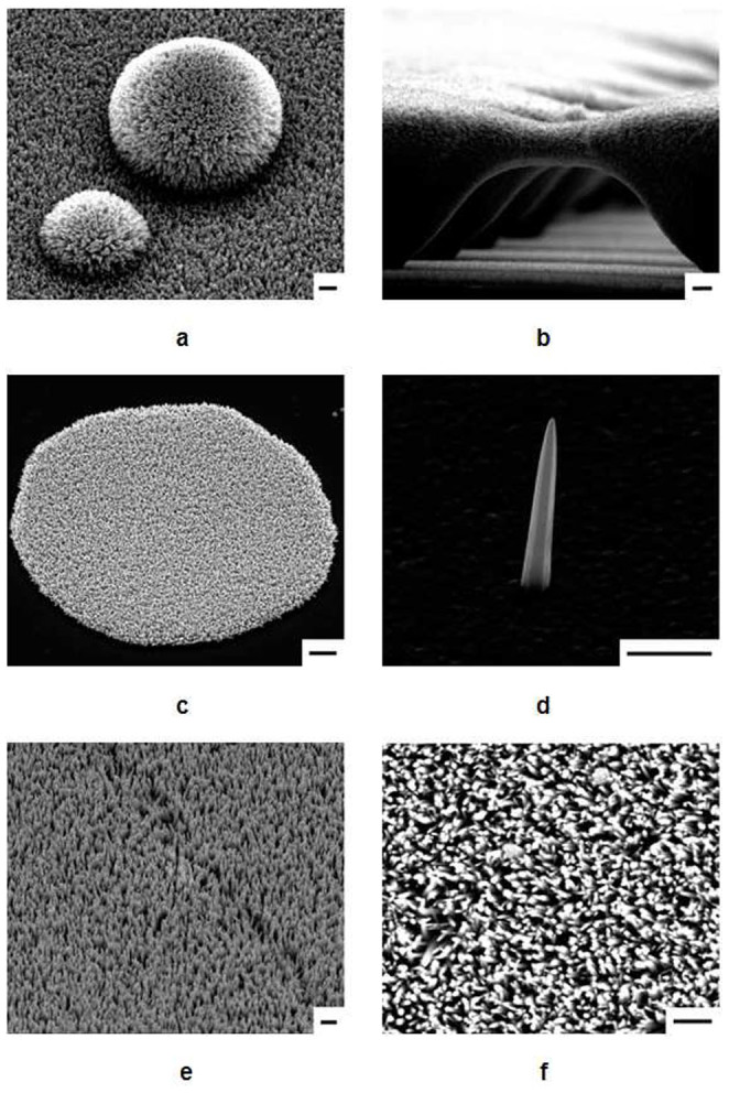
(a–f), SEM images of ZnO nanowires grown on (a) PET, (b) SU-8, (c) silicon, (d) polyimide, (e) PDMS, and (f) parylane-C. The concentration of the zinc nitrate hexahydrate and HMT solution was 20 mM, and the initial pH values were 9 ~ 9.5. Scale bars represent 1 μm.
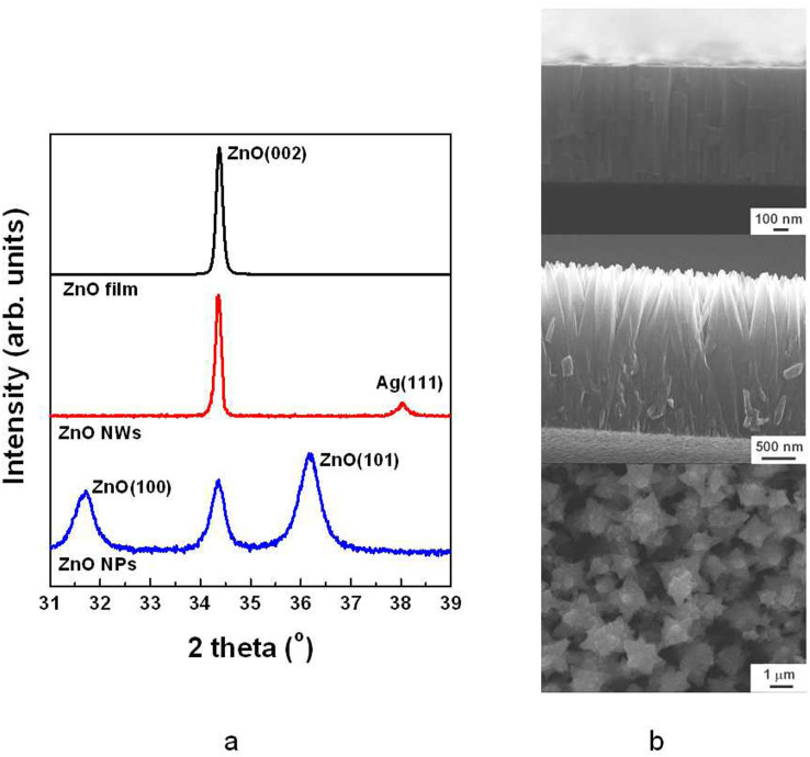
We determined the crystallinity of the ZnO nanowires by performing X-ray diffraction (XRD). Figure 2a shows the XRD patterns of a pure ZnO film deposited on a silicon (001) substrate using an RF sputtering system (black line), ZnO nanowires grown on an oxidized silver film on a polyimide substrate (red line), and ZnO nanoparticles grown in the nutrition solution (blue line). The ZnO film deposited at a high temperature of 300°C contains a peak at approximately 34.38° that corresponds to the (0002) spacing of the wurtzite structure of ZnO; the occurrence of this peak indicates preferential alignment in the c-axis direction. For the ZnO nanowires on the Ag film, two XRD peaks were observed at approximately 34.36° and 38.04°; these peaks indicate vertically grown ZnO (0002) and Ag (111), respectively. In the hexagonal structure of ZnO, the plane spacing is related to the lattice constants a and c and to the Miller indices by the relation  , with the first-order approximation n = 1,
  . For the (002) orientation at 2θ = 34.38° and 34.36°, the lattice constant c was estimated to be 0.5213 nm and 0.5216 nm, respectively, according to
  . The c-value of strain-free bulk ZnO is 0.5205 nm28, which is smaller than the corresponding values of ZnO/Si and ZnO nanowire/Ag. This result means that the ZnO film and ZnO nanowires have similar tensile stresses. Although ZnO nanowires were grown on a flexible polyimide substrate, the half-maximum full wavelength (i.e., the full-width at half-maximum, FWHM) of the peak in XRD pattern of the ZnO nanowires (0.14°) is slightly narrower than that of the ZnO film (0.15°). The peak positions and FWHMs obtained from the ZnO film and the ZnO nanowires indicate that the lattice mismatch of ZnO nanowires on oxidized silver is similar to that of the ZnO film on silicon. Normally, the lattice constant of diamond-structured silicon is 0.543 nm. The mismatch between silicon (001) and ZnO (002) is estimated to be 104.16%. However, silver (111) with an FCC crystal structure has a lattice constant of 0.4094 nm, as calculated by
  29. If ZnO nanowires are grown on pure Ag (111), then the lattice mismatch is evaluated as 78.49%. This result means that ZnO (002) on Ag (111) has a compressive stress and must exhibit a lower XRD peak position than pure ZnO (002). Naturally oxidized silver on polyimide shows an XRD peak position of 34.32° related to Ag2O (111) (Supplementary Fig. S2). This peak is similar to that of ZnO (002), which indicates a low lattice mismatch between Ag2O and ZnO. Unlike these two cases, ZnO nanoparticles exhibited broad XRD peaks at 31.69°, 34.36°, and 36.16° because ZnO nanoparticles consist of large polycrystalline grains. Since ZnO nanoparticles were self-synthesised in solution, the growth directions are (100), (002), and (101), as shown in Fig. 2a (blue line). In addition, structural properties of ZnO film, nanowires, and nanoparticles are clearly distinguishable from each other as shown in SEM images of Fig. 2b.
Figure 2. XRD analysis and SEM images of a ZnO film, ZnO nanowires (NWs), and ZnO nanoparticles (NPs).
(a) The ZnO film (black line) was deposited by an RF sputtering system, ZnO nanowires (red line) were grown on naturally oxidised silver, and ZnO nanoparticles (blue line) were self-synthesised in solution by the hydrothermal growth method. (b) SEM images of ZnO film (top), ZnO nanowires (middle), and ZnO nanoparticles (bottom).
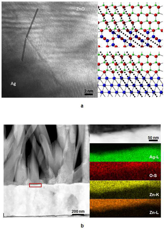
In addition, we used a conventional transmission electron microscope to further examine the structure of ZnO nanowires grown on naturally oxidized silver on a Cu grid. The ZnO nanowires were grown for 3 hours in a 40 mM solution at pH 9 with 4 g of PEI. A high-magnification TEM image of the interfacial region of a ZnO nanowire and oxidized silver is shown in Fig. 3a. The atomic lines at the ZnO/Ag interface region are curved with a certain angle. Figures 3b and 3c are structural models showing the interface between ZnO and Ag (or Ag2O) as a function of the crystallographic direction. The Ag has a faced centred space group of Fm-3m and a = 0.40853 nm30, whereas Ag2O has cuprite cubic structure with a space group of P-3m1 and a = 0.4736 nm31. The ZnO has a hexagonal space group of P63mc with a = 0.3250 nm and c = 0.5207 nm32. As shown in Fig. 3b, the interface bound by ZnO (0002) and Ag2O (111) clearly shows the regularity of the Ag–O–Zn bonds due to their similar lattice parameters. The curved atomic lines are in good agreement with the TEM analysis. However, the interface directly contacted by ZnO (0002) and Ag (111) does not show any regularity in Ag–O–Zn bonds due to the large difference in lattice parameters between these two materials. This irregular interface may result in interfacial stress and defect formation. The lattice mismatch at the nanowire–substrate interface has a dominant effect on the tendency of nanowires towards either vertical or random epitaxial growth on heterogeneous structures. High structural strain due to a high degree of lattice mismatch makes the nucleation and growth of a nanowire on a substrate impossible32. Most nanowires that have been successfully grown on substrates have lattice mismatches of less than 12%33. Nanowires with larger lattice mismatches with the substrate tend not to grow in the vertical <111> direction, whereas materials with minimal lattice mismatches can readily grow in the vertical <111> direction. A change in the growth direction between vertical and non-vertical <111> directions may serve as a means to relieve strain at the nanowire–substrate interface and may explain the large yield of non-vertical nanowires in material systems with large lattice mismatches. Therefore, we believe that the lattice constant of oxidized silver is matched as an interlayer between ZnO and pure Ag. This result is in good agreement with the XRD data in Supplementary Fig. S2, which indicates that the oxidized silver layer is too thin and that the peaks of oxidized silver and ZnO could overlap.
Figure 3. Structural properties of ZnO nanowires on an oxidised silver layer.
(a), High-magnification TEM image of ZnO nanowires on the Ag layer. (b–c), Structural models showing the interface between the ZnO and (b) Ag2O and (c) Ag layers. (d), STEM image of a ZnO nanowire on oxidised silver. (e), STEM image and XEDS mapping images taken from the interfacial region between the ZnO nanowire and oxidised silver.
An additional analysis was conducted using scanning TEM (STEM) and X-ray energy-dispersive spectroscopy (XEDS) mapping (red coloured box) at the interfacial region between ZnO and oxidized silver, as shown in Figs. 3d and 3e. An additional analysis was conducted using STEM and XEDS appear at the localized ZnO and Ag portions of the interface. Interestingly, the spatial distribution of the O-S shell is not atomically abrupt and is found deep inside the Ag layer, indicating the formation of silver oxide.
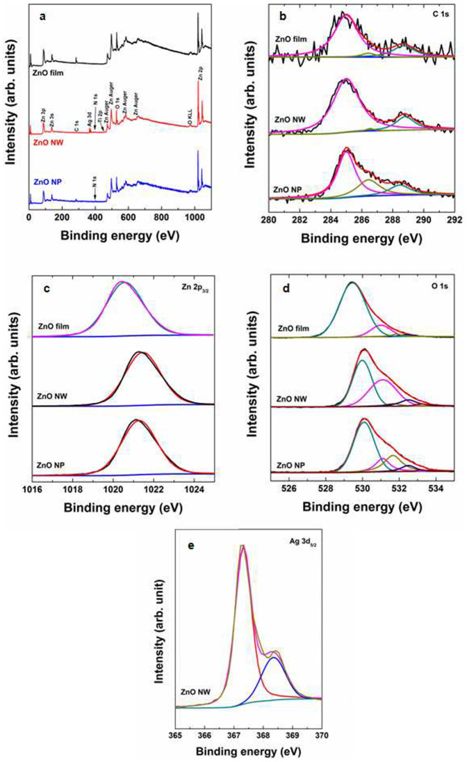
To accurately determine whether an oxidized interlayer exists between the Ag film and the ZnO nanowire, we used X-ray photoelectron spectroscopy (XPS) to characterize the composition of a pure ZnO film deposited on silicon, ZnO nanowires grown on an oxidized silver film, and ZnO nanoparticles grown in solution. Figure 4a presents the XPS spectra of the pure ZnO film, the ZnO nanowires, and the ZnO nanoparticles, which indicate the presence of Zn, O, Ag, Ti, N, and C. Titanium results from the thin Ti layer present as an underlayer of Ag. As shown in Fig. 4b, the binding energy (BE) scale was calibrated using the carbon peak (C-1s) at 285 eV as a reference34,35. As these samples were exposed to ambient air prior to the XPS analysis, small amounts of carbonyl compounds (CO and CO2) were observed, resulting in two additional peaks at 286.6 and 288.7 eV36,37,38, respectively. Those peaks arising from carbonyl compounds were also used as a reference to identify the different O-related species present in the samples. The pure ZnO film exhibited a Zn-2p3/2 core level with a peak position of 1020.58 eV, as shown in Fig. 4c. However, the Zn-2p levels of the ZnO nanowires were shifted to higher binding energies towards 1021.46 eV, whereas those of the ZnO nanoparticles were 1021.28 eV. BE shifts of +0.88 eV for the ZnO nanowires and +0.70 eV for the ZnO nanoparticles were measured with respect to the Zn-2p BE of the pure ZnO film. The shifts of the Zn-2p peaks toward high energy suggests the presence of additional chemical states of Zn, indicating a decrease in the number of Zn atoms bound to oxygen due to the deposition of ZnO in an oxygen-rich environment39,40,41. In addition, a similar phenomenon was observed for the formation of Ag–O–Zn bonds42,43.
Figure 4. Chemical composition of ZnO samples.
(a), Survey XPS spectra of ZnO film, nanowires, and nanoparticles, including Zn, O, Ag, Ti, N, and C. (b–e), XPS spectra corresponding to the (b) C-1s, (c) Zn-2p3/2, (d) O-1s, and (e) Ag-3d5/2 core levels of a pure ZnO film, ZnO nanowires, and ZnO nanoparticles. The ZnO nanowires were grown on oxidised silver on a polyimide substrate.
Figure 4d presents the asymmetric peaks observed in the O-1s region deconvoluted by several subspectral components: (i) ZnO, (ii) defective ZnOx or ZnOH, (iii) Ag2O or Ag–O–Zn, or adsorbed oxygen species, (iv) CO (531.1 eV), and (v) CO2 (532.5 eV). In addition to the CO and CO2 signals, the pure ZnO film exhibits two additional peaks at 529.55 eV and 531.96 eV, which were assigned to O ions in stoichiometric Zn–O–Zn and to an oxygen-deficient ZnOx region44,45, respectively. To determine the stoichiometry of ZnOx(OH)y, we estimated the O-1s/Zn-2p ratio of the ZnO film to be 1.25, whereas those of the ZnO nanowires and ZnO nanoparticles were calculated to be 1.27 and 1.48, respectively. In addition to peaks related to stoichiometric ZnO, defective ZnO or ZnOH, CO, and CO2, an additional small feature at 533.2 eV was observed in the spectra of ZnO nanowires and nanoparticles. This feature could be assigned to Ag–O bonds or to bonds related to adsorbed oxygen species (i.e., H2O or adsorbed O2). As discussed for the XRD analysis, however, no evidence of a significant increase in the lattice parameter c was found when Zn2+ ions were replaced by Ag+ ions because of the larger radius of Ag+ ions (0.126 nm) compared with Zn2+ ions (0.074 nm).
The Ag-3d BE region (Fig. 4e) consists of an asymmetric peak that could be fitted with a doublet tentatively assigned to the Ag-3d5/2 core levels of two different species: Ag2O (367.32 eV, 75.04% of the total Ag XPS signal) and Ag (368.35 eV, 24.96%)46. Theoretically, the deposited silver is spontaneously oxidized by atmospheric oxygen at room temperature in the chemical reaction 4Ag (s) + O2 → 2Ag2O (s). The standard-state enthalpy ( ) and entropy (
 ) changes for this reaction are −62.2 kJ and −0.133 kJ/K, respectively, as calculated from the thermodynamic data47. These values indicate that the reaction is exothermic and that the entropy of the reaction is negative. The standard Gibbs free energy (
 ) of the reaction can be calculated as
  , where R and P are the ideal gas constant and the gas pressure, respectively. At 298 K and 1 atm, the Gibbs free energy is estimated to be −22.6 kJ. Therefore, the Ag2O present on silver exposed to the natural oxygen environment is naturally formed48,49.
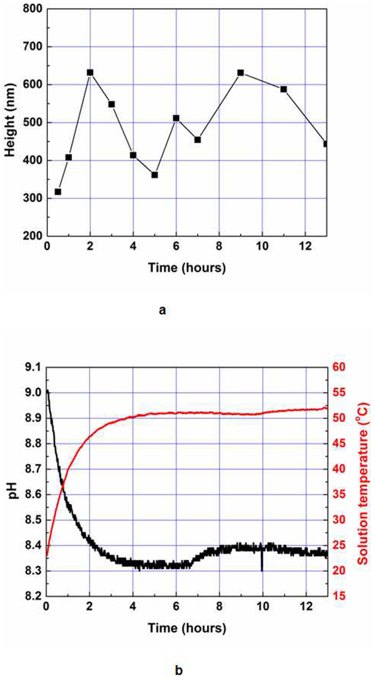
The dependence of the average nanowire height on growth time is illustrated in Fig. 5a. The solution was fixed to a concentration of 20 mM. Two distinct growth kinetics can be observed: a rapid step, which takes less than 2 hours, with a growth rate of 5.27 nm/min; and a fluctuation in the kinetics of nanowire growth due to lower super-saturation of precursors. To understand the growth mechanism, we measured the pH value and solution temperature as a function of growth time. The initial pH value was set to 9, and the hot-plate temperature was fixed at 90°C. The difference between the set temperature and the solution temperature resulted from the poor thermal conductivity of the glass and the aqueous solution, as shown in Fig. 5b. In the initial stage, the pH value decreased due to the protonation of the solution by heating. The relationship between pH and the fluctuating growth pattern of ZnO nanowires observed in Fig. 5a can be interpreted as indicating that the ZnO nanowires stop growing at a pH value of approximately 8.4. When the pH value falls below 8.4, the length of the ZnO nanowires decreases due to the dissolution of the nanowires back into the solution50.
Figure 5. Growth of ZnO nanowires as a function of time, pH, concentration, and temperature.
(a), Average ZnO nanowire heights as a function of reaction time. The concentration of a nutrition solution and setting temperature were 20 mM and 90°C, respectively. (b), In situ pH value and solution temperature as functions of reaction time and molar concentration. The set temperature was 90°C. The average heights of ZnO nanowires were measured from cross-sectional SEM images.
Discussion
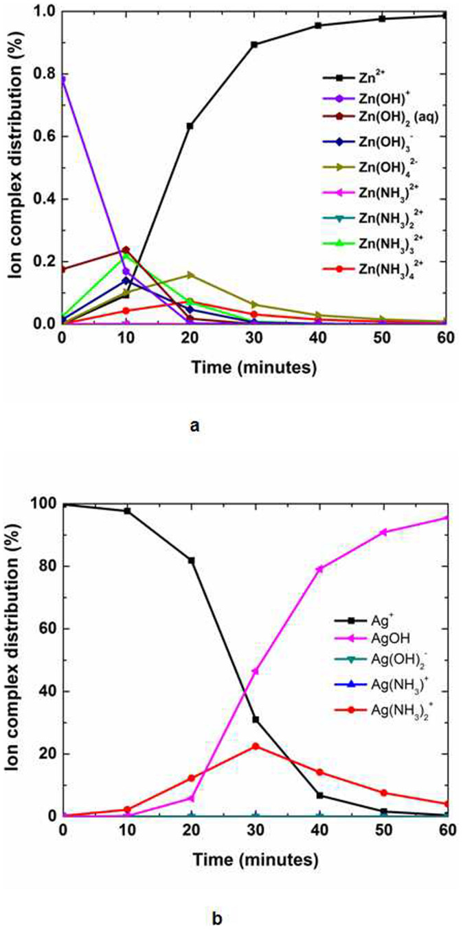
To understand the reaction kinetics in detail, we calculated the speciation diagram of intermediate metal hydroxide and amine complexes from known constants51. Figures 6a and 6b show the ion complex distribution of Zn2+ and Ag+ ions using the time, solution temperature, and pH values determined from the calculated speciation diagrams. Silver(I) ions are normally generated from Ag2O in aqueous solution because pure silver cannot be ionized in aqueous solution. In the initial stage, Zn2+ ions are mostly converted into Zn(OH)+ and Zn(OH)2, whereas Ag+ ions are dominant in solution. The presence of Ag+ ions on the surface can attract negative ions such as OH−, Zn(OH)3−, and Zn(OH)42− through Coulombic attraction rather than positive or neutral ions such as NH3+, Zn+, Zn(OH)+, and Zn(OH)2. However, because the amine complexes are strongly adsorbed due to their high solubility at high pH, the Ag+ can rapidly form more [Ag(NH3)2]+ than AgOH in the initial growth stage, as shown in Fig. 6b. To understand the effect of protonation in solution, we measured the pH values of a 20 mM zinc nitrate hexahydrate and hexamethylenetetramine (HMT) solution with an oxidized silver film on a polyimide substrate, as shown in Supplementary Fig. S5. For reference, pH values were also measured in the same reaction solution without an oxidized silver film. All solutions were measured at room temperature and were fixed at an initial pH value of 9 with additional ammonium hydroxide. The pH values of all solutions rapidly decreased in the initial stage due to the increase in protons. For the growth of ZnO in an aqueous mixture of zinc nitrate hexahydrate, hexamethyleneimine, and ammonium hydroxide, the possible reactions are  and [Zn(NH3)4]2+ + 3H2O ⇒ ZnO + 2NH4+ 2NH3·H2O52,53. However, the second reaction produces ammonium hydroxide, which can subsequently react with water to produce hydroxide ions via the reaction NH3 + H2O ⇒ NH4+ + OH−. This reaction means that the pH of the mixture would increase with reaction time. Therefore, the main ZnO reaction that occurs in the initial stage of this experiment is the first reaction because the pH value of the solution with an oxidized silver film decreases with reaction time, as shown in Fig. 6c. Because this reaction can produce ammonia to increase the pH value via the equation 2[Ag(NH3)2]+ + 2OH− ⇒ Ag2O + 4NH3 + H2O, this reaction is also inconsistent with the rapid decrease in pH observed in the initial reaction stage. Notably, many metal oxides would hydrolyse in the presence of water to form hydroxide layers at the surface (≡M–OH). An oxide or hydroxide surface (≡M–OH) can become charged by reacting with H+ or OH− ions due to surface amphoteric reactions54. Therefore, Ag+ ions on the Ag2O surface can form Ag–OH. Interestingly, Ag+ and Zn2+ ions are known as B-type metal cations with low electronegativities55, i.e., in the case of Ag–OH, the bond length of Ag–O is shorter than that of O–H because Ag (χAg = 1.93) is less electronegative than H (χH = 2.20). In water, OH− can convert Ag–OH into Ag–O− + H2O. At the same time, Zn2+ ions with a low electronegativity (χZn = 1.65) near Ag–O− can be easily bonded to form Ag–O–Zn+. After Zn+ ions are chemisorbed onto the Ag2O surface, Zn+ ions bond oxygen ions to form ZnO. Then, ZnO can fully cover the Ag2O surface in aqueous Zn(NO3)2–HMT–ammonia solution and ZnO nanowires can grow further through hydrothermal synthesis, as shown by further SEM analysis (Supplementary Fig. S6).
Figure 6. Reaction kinetics of ZnO and Ag2O.
(a–b), Ion complex distribution of (a) Zn2+ and (b) Ag+ ions as functions of time, temperature, and pH using the data from Figure 5.
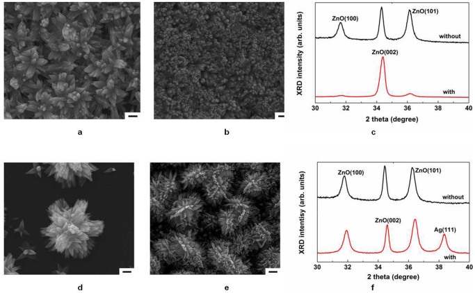
To understand the effect of silver catalyst on other metals, we selected a titanium film, which has a low electronegativity (χTi = 1.54), and a molybdenum film, which has a high electronegativity (χMo = 2.16), and deposited both by RF sputtering onto polyimide films. On the titanium substrate, ZnO nanowires partially grew without any help from the Ag catalyst, and the ZnO nanowires grown on Ti substrates became more dense and c-oriented when the Ag catalyst was used. Although the surface of Ti can be easily oxidized due to its low electronegativity, Ag catalyst treatment can effectively oxidize the surface of Ti because Ag is a well-known oxidation agent and can ionize the surface of the Ti substrate, enabling it to bond to hydroxide anions. These results are in good agreement with XRD data for ZnO nanowires with and without Ag catalyst treatment. No Ag-related XRD peaks were observed in the pattern of the Ag catalyst-treated Ti surface. The rutile type crystal structure of TiO2 is well known to have a tetragonal structure with space group P42/mnm and a = 0.4594 nm56. Interestingly, the tetragonal structure can be combined with a hexagonal structure. In addition, because the Ti substrate has the same lattice as TiO2, the lattice constant c of ZnO becomes close to that of bulk ZnO when ZnO nanowires are grown on a Ag-treated Ti substrate, as shown in Fig. 7c. For molybdenum, however, ZnO nanowires were not grown because the electronegativity of Mo is larger than those of the other materials and because the surface of Mo easily loses adsorbed oxygen ions to the solution. To overcome this problem, we employed both oxygen-plasma and Ag-catalyst treatments to oxidize a Mo metal surface. As shown in the SEM image in Fig. 7e, randomly grown ZnO nanowires fully covered the oxidized Mo surface. Unlike the case of Ti substrates, the Ag peak in the XRD pattern of the Mo substrate indicates that self-synthesized Ag particles may adhere to the rough surface of ZnO nanowires grown on the Mo substrate. This phenomenon was also observed on the Cu substrate, as shown in Supplementary Fig. S8. The ZnO nanowires were randomly grown due to the crystal structure of Mo, which has a body-centred cubic structure with a space group of Im-3m and a = 0.3147 nm31. Although MoO2 has a tetragonal structure with a space group of P42/mnm and a = 0.487 nm31, the Mo substrate can compress the thin MoO2 interlayer formed by plasma and Ag-catalyst treatments due to the large lattice mismatch between Mo and MoO2. This stressed MoO2 interlayer can affect the growth direction of ZnO nanowires. This stress was observed in the XRD data (Fig. 7f), where the ZnO (002) peak shifted from 34.42° to 34.60°, thereby indicating an increased ZnO lattice constant.
Figure 7. Plasma and Ag catalyst treatments.
(a–c), SEM images of ZnO nanowires on a titanium substrate (a) without and (b) with Ag catalyst treatment; (c) XRD data of ZnO nanowires on a titanium substrate with (black line) and without (red line) Ag catalyst treatment. (d–f), SEM images of ZnO nanowires on molybdenum substrates (d) without and (e) with both plasma and Ag-catalyst treatments; (f) XRD data of ZnO nanowires on molybdenum substrate with (black line) and without (red line) Ag-catalyst treatment. For the Ag catalyst treatment, 1 mM silver nitrate was added to 40 mM nutrition solutions for samples with Ti and Mo films. Molybdenum films were also treated with oxygen plasma. Scale bars represent 1 μm.
The unique properties of oxidized silver lead to highly controlled growth of ZnO nanowires on various substrates. The oxidized silver films provide a surprisingly good lattice-matched structure with ZnO. Ionized Ag strongly attracts negatively charged Zn ion complexes by Coulombic forces to nucleate ZnO on a silver oxide film. Other metal substrates have been used as heterogeneous growth substrates for ZnO nanowires with the help of plasma and Ag-catalyst treatments. This low-temperature synthetic method has the potential to support numerous important applications by enabling the well-controlled synthesis of ZnO nanowires on any substrate.
Methods
ZnO nanowires were grown on various organic and inorganic substrates with a naturally oxidized silver layer, deposited by RF sputtering, in aqueous 1:1 solutions of zinc nitrate hexahydrate (Sigma Aldrich) and hexamethylenetetramine (Sigma-Aldrich). Ammonium hydroxide (Fisher) was added to obtain certain initial pH values. PEI (Sigma-Aldrich) was used to localize the growth of the ZnO nanowires. The nanowires were grown in a conventional oven or on a hot plate. In situ pH values and solution temperatures were measured using a BK pH meter (model 760) and an Omega thermocouple probe (TJ-USB), respectively. The PET substrate was a 3M™ multipurpose transparency film. Bridge-shaped arrays were prepared from SU-8 (Microchem) using conventional photolithography techniques. Polyimide substrates applied on glass slides were 1 mil Kapton® tapes made from DuPont™ Kapton® HN film with silicone adhesive. The Ag particle film was deposited onto PDMS using a 1 mM solution of AgNO3 in ethanol for 1 hour. The Ag particle film was then exposed to ambient air for 2 hours. Characterization was performed using scanning electron microscopy (FEI QUANTA FEG 600 ESEM), transmission electron microscopy (FEI Tecnai F30 G2 Twin Microscope), X-ray diffractometry (PANalytical X'Pert PRO, Cu Kα and a Rigaku MiniFlex 600, Cu Kα), and X-ray photoelectron spectroscopy (Kratos Axis 165).
Author Contributions
B.H.K. and J.W.K. performed the experiments, analysed the data, discussed the results and commented on the manuscript. J.W.K. conceived and supervised this study, and provided intellectual and technical guidance.
Supplementary Material
supplementary information
Acknowledgments
This work was partially supported by the Los Alamos National Laboratory and the Strategic Investment Allocation Fund. The authors would like to thank the team members, R. Almeida, J. Jiao, C. Kirkendall, B. Nullmeyer, Q. Nguyen, and D. Howard for their helpful assistances. We are grateful for useful discussions for XPS analysis with Mr. Brian Porter in the Material Research Center at the Missouri University of Science and Technology.
References
- Prete P. Nanowires. (Intech, Rijeka, Croatia, 2010). [Google Scholar]
- Sattler K. D. Handbook of nanophysics: nanotubes and nanowires. (CRC Press, Boca Raton, FL, 2010). [Google Scholar]
- Wang Z. L. Nanowires and nanobelts: materials, properties and devices. (Kluwer Academic Publishers, Norwell, MA, 2013). [Google Scholar]
- Litton C. W., Reynolds D. C. & Collins T. C. Zinc oxide materials for electronic and optoelectronic device applications. (John Wiley & Sons. Hoboken, NJ, 2011). [Google Scholar]
- Look D. C., Claflin B., Alivov Y. I. & Park S. J. The future of ZnO light emitters. Phys. Status Solidi A 201, 2203–2212 (2004). [Google Scholar]
- Li M. et al. The research on suspended ZnO nanowire field-effect transistor. Chin. Phys. B 18, 1594–1597 (2009). [Google Scholar]
- Sun B. Q. & Sirringhaus H. Surface tension and fluid flow driven self-assembly of ordered ZnO nanorod films for high-performance field effect transistors. J. Am. Chem. Soc. 128, 16231–16237 (2006). [DOI] [PubMed] [Google Scholar]
- Ju S. Y. et al. Fabrication of fully transparent nanowire transistors for transparent and flexible electronics. Nature Nanotech. 2, 378–384 (2007). [DOI] [PubMed] [Google Scholar]
- Hsu C. L. & Tsai T. Y. Fabrication of fully transparent indium-doped ZnO nanowire field-effect transistors on ITO/glass substrates. J. Electrochem. Soc. 158, K20–K23 (2011). [Google Scholar]
- Ko S. H. et al. Nanoforest of hydrothermally grown hierarchical ZnO nanowires for a high efficiency dye-sensitized solar cell. Nano Lett. 11, 666–671 (2011). [DOI] [PubMed] [Google Scholar]
- Tian B. Z. et al. Coaxial silicon nanowires as solar cells and nanoelectronic power sources. Nature 449, 885–890 (2007). [DOI] [PubMed] [Google Scholar]
- Yang X. et al. Nitrogen-doped ZnO nanowire arrays for photoelectrochemical water splitting. Nano Lett. 9, 2331–2336 (2009). [DOI] [PubMed] [Google Scholar]
- Kong Y. C. et al. Ultraviolet-emitting ZnO nanowires synthesized by a physical vapor deposition approach. Appl. Phys. Lett. 78, 407–409 (2001). [Google Scholar]
- Chang P. C. et al. ZnO nanowires synthesized by vapor trapping CVD method. Chem. Mater. 16, 5133–5137 (2004). [Google Scholar]
- Zheng M. J., Zhang L. D. & Shen W. Z. Fabrication and optical properties of large-scale uniform zinc oxide nanowire arrays by one-step electrochemical deposition technique. Chem. Phys. Lett. 363, 123–128 (2002). [Google Scholar]
- Greene L. E. et al. Low-temperature wafer-scale production of ZnO nanowire arrays. Angew. Chem. 42, 3031–3034 (2003). [DOI] [PubMed] [Google Scholar]
- Xu S. et al. Patterned growth of vertically aligned ZnO nanowire arrays on inorganic substrates at low temperature without catalyst. J. Am. Chem. Soc. 130, 14958–14959 (2008). [DOI] [PubMed] [Google Scholar]
- Joo J. et al. Face-selective electrostatic control of hydrothermal zinc oxide nanowire synthesis. Nature Mater. 10, 596–601 (2011). [DOI] [PMC free article] [PubMed] [Google Scholar]
- Yeo J. et al. Rapid, one-step, digital selective growth of ZnO nanowires on 3D structures using laser induced hydrothermal growth. Adv. Funct. Mater. 23, 3316–3323 (2013). [Google Scholar]
- Park H. H. et al. Position-controlled hydrothermal growth of ZnO nanorods on arbitrary substrates with patterned seed layer via ultraviolet-assisted nanoimprint lithography. CrystEngComm. 15, 3463–3469 (2013). [Google Scholar]
- He Y. et al. Crystal-plane dependent of critical concentration for nucleation on hydrothermal ZnO nanowires. J. Phys. Chem. C 117, 1197–1203 (2013). [Google Scholar]
- Zhu R., Zhang W., Li C. & Yang R. Uniform zinc oxide nanowires arrays grown on nanoepitaxial surface with general orientation control. Nano Lett. 13, 5171–5176 (2013). [DOI] [PubMed] [Google Scholar]
- Zheng Z. et al. General route to ZnO nanorod arrays on conducting substrates via galvanic-cell-based approach. Sci. Rep. 3, 2434 (2013). [DOI] [PMC free article] [PubMed] [Google Scholar]
- Greene L. E. et al. General route to vertical ZnO nanowire arrays using textured ZnO seeds. Nano Lett. 5, 1231–1236 (2005). [DOI] [PubMed] [Google Scholar]
- Liu J. et al. Ultrathin seed-layer for tuning density of ZnO nanowire arrays and their field emission characteristics. J. Phys. Chem. C 112, 11685–11690 (2008). [Google Scholar]
- Öztekin N., Alemdar A., Güngör N. & Erim F. B. Adsorption of polyethylemeimine from aueous solutions on bentonite clays. Mater. Lett. 55, 73–76 (2002). [Google Scholar]
- Chen L. Y., Yin Y. T., Chen C. H. & Chiou J. W. Influence of polyethyleneimine and ammonium on the growth of ZnO nanowires by hydrothermal method. J. Phys. Chem. C 115, 20913–20919 (2011). [Google Scholar]
- Puchert M. K., Timbrell P. Y. & Lamb R. N. Postdeposition annealing of radio frequency magnetron sputtered ZnO films. J. Vac. Sci. Technol. A 14, 2220–2230 (1996). [Google Scholar]
- Stock S. R. & Cullity B. D. Elements of X-ray diffraction. (Prentice Hall, Upper Saddle River, NJ, 2001). [Google Scholar]
- Zhou G. et al. Surfactant-assisted synthesis and characterization of silver nanorods and nanowires by an aqueous solution approach. J. Cryst. Growth 289, 255–259 (2006). [Google Scholar]
- Villars P. & Calvert L. D. Pearson's handbook of crystallographic data for intermetallic phases. (American Society for Metals, Metals Park, OH, 1985). [Google Scholar]
- Chen C. et al. Hierarchical Assembly of ZnO Nanostructures on SnO2 Backbone Nanowires: Low-Temperature Hydrothermal Preparation and Optical Properties. ACS Nano 3, 3069 (2009). [DOI] [PubMed] [Google Scholar]
- Fortuna S. A. & Li X. Metal-catalyzed semiconductor nanowires: a review on the control of growth directions. Semicon. Sci. Technol. 25, 024005 (2010). [Google Scholar]
- Lupan O. et al. Effects of annealing on properties of ZnO thin film prepared electrochemical deposition. Appl. Surf. Sci. 256, 1895–1907 (2010). [Google Scholar]
- Nefedov V. I., Salyn Y. V., Leonhardt G. & Scheibe R. A comparison of different spectrometers and charge corrections used in X-ray photoelectron spectroscopy. J. Electron Spectrosc. Relat. Phenom. 10, 121–124 (1977). [Google Scholar]
- Kawase K. et al. XPS Study of H-Terminated Silicon Surface under Inert Gas and UHV Annealing. J. Electrochem. Soc. 152, G163–G167 (2005). [Google Scholar]
- Joubert O., Pelletier J., Fiori C. & Tan T. A. N. Surface mechanisms in O2 and SF6 microwave plasma etching of polymers. J. Appl. Phys. 67, 4291 (1990). [Google Scholar]
- Salaneck W. R., Paton A. & Clark D. T. Double mass transfer during polymer-polymer contacts. J. Appl. Phys. 47, 144 (1976). [Google Scholar]
- Zhang Y. et al. X-ray photoelectron spectroscopy study of ZnO films grown by metal-organic chemical vapor deposition. J. Cryst. Growth 252, 180 (2003). [Google Scholar]
- Li H. et al. Influence of annealing on ZnO films grown by metal–organic chemical vapor deposition. Mater. Lett. 58, 3630 (2004). [Google Scholar]
- Core G. E. B. et al. Characterization of pure ZnO thin films prepared by a direct photochemical method. J. NonCryst. Solids 352, 4088–4092 (2006). [Google Scholar]
- Shin M. H. et al. Effect of doping elements on ZnO etching characteristics with CH4/H2/Ar plasma. Thin Solid Films 515, 4950–4954 (2007). [Google Scholar]
- Lupan O. et al. Synthesis and characterization of Ag- or Sb-doped ZnO nanorods by a facile hydrothermal route. J. Phys. Chem. C 114, 12401–12408 (2010). [Google Scholar]
- Duan L. et al. Enhancement of ultraviolet emissions from ZnO films by Ag doping. Appl. Phys. Lett. 88, 232110 (2006). [Google Scholar]
- Armelao L., Fabrizio M., Gialanella S. & Zordan F. Sol–gel synthesis and characterisation of ZnO-based nanosystems. Thin Solid Films 394, 90 (2001). [Google Scholar]
- Bielmann M. et al. AgO investigated by photoelectron spectroscopy: Evidence for mixed valence. Phys. Rev. B 65, 235431 (2001). [Google Scholar]
- Lide D. R. & Haynes W. M. CRC Handbook of chemistry and physics. (CRC press, Boca Raton, FL, 2009). [Google Scholar]
- de Rooij A. The Oxidation of silver by atomic oxygen. ESA Journal 3, 363–382 (1989). [Google Scholar]
- Reicho A., Stierle A., Costina I. & Dosch H. Stranski-Krastanov like oxide growth on Ag(111) at atmospheric oxygen pressures. Surf. Sci. 601, L19–L23 (2007). [Google Scholar]
- Kwon J. W. & Kim E. S. Fine ZnO Patterning with Controlled Sidewall-Etch Front Slope. J. Microelectromech. Syst., 3, 603–609 (2005). [Google Scholar]
- Stumm W. & Morgan J. J. Aquatic chemistry. (John Wiley & Sons, Hoboken, NJ, 1996). [Google Scholar]
- Li W. J., Shi E. W., Zhong W. Z. & Yin Z. W. Growth mechanism and growth habit of oxide crystals. J. Cryst. Growth 203, 186–196 (1999). [Google Scholar]
- Kim K. S., Jeong H. J., Jeong M. S. & Jung G. Y. Polymer-templated hydrothermal growth of vertically aligned single-crystal ZnO nanorods and morphological transformations using structural polarity. Adv. Func. Mater. 20, 3055–3063 (2010). [Google Scholar]
- Degen A. & Kosec M. Effect of pH and impurities on the surface charge of zinc oxide in aqueous solution. J. Eur. Ceram. Soc. 20, 667–673 (2000). [Google Scholar]
- Stumm W. Chemistry of the solid-water interface. (John Wiley & Sons, Hoboken, NJ, 1992). [Google Scholar]
- De Graef M. & McHenry M. E. Structure of materials. (Cambridge University Press, New York, 2007). [Google Scholar]
Associated Data
This section collects any data citations, data availability statements, or supplementary materials included in this article.
Supplementary Materials
supplementary information


