Abstract
A unique CMOS chip has been designed to serve as the front-end of the tracking detector data acquisition system of a pre-clinical prototype scanner for proton computed tomography (pCT). The scanner is to be capable of measuring one to two million proton tracks per second, so the chip must be able to digitize the data and send it out rapidly while keeping the front-end amplifiers active at all times. One chip handles 64 consecutive channels, including logic for control, calibration, triggering, buffering, and zero suppression. It outputs a formatted cluster list for each trigger, and a set of field programmable gate arrays merges those lists from many chips to build the events to be sent to the data acquisition computer. The chip design has been fabricated, and subsequent tests have demonstrated that it meets all of its performance requirements, including excellent low-noise performance.
Keywords: Application specific integrated circuits, computed tomography, low-noise amplifiers, mixed analog digital integrated circuits, particle tracking, silicon radiation detectors
I. INTRODUCTION
PROTON COMPUTED TOMOGRAPHY (pCT [1]) holds promise to improve treatment planning for hadron therapy [2] by reconstructing an accurate map of the stopping power in the tissue in front of and inside the tumor. That would eliminate the need to translate X-ray attenuation data into proton stopping power. However, the implementation of pCT proposed in [1] (and also by others, such as in [3]) requires the proton trajectories and energies to be measured one particle at a time. To accomplish that in an acceptable clinical time frame will require a tracking system that can measure the order of a million protons per second.
We are building such a system [4] to operate in the proton-synchrotron beam of the Loma Linda University Medical Center [5]. There the protons will arrive in bunches spaced at ~110 ns intervals. Due to limitations of the energy detector, which unlike the tracker cannot handle multi-track events, we are interested only in single-proton bunches. That limits the practical trigger rate to about 1 MHz, for which about 7.5% of the acquired events will contain more than one proton. Our system design can accommodate trigger rates up to at least 2 MHz, but of course with corresponding increases in the percentage of events containing multiple protons.
Silicon strip detectors (SSD) are nearly ideal candidates for the tracking portion of a pCT system. The relatively high cost per cm of the sensors (relative to plastic scintillators, for example) is more than offset by their high performance, reliability, stability, and ease of assembly. Furthermore, the raw sensor cost would be a minor portion of the overall cost of a clinical system. Silicon strip detectors offer the following attractive characteristics, demonstrated in very large systems such as the Fermi-LAT Gamma-ray Space Telescope [6] and the CERN LHC tracking detectors [7], [8]:
Near 100% efficiency for particle detection with effectively zero noise occupancy.
Inherently fine spatial resolution.
All solid-state, with simple calibration that can be stable over time periods of years.
Compact and easy assembly using standard industry processes, with excellent mechanical stability.
However, SSDs do require specialized electronics for their front-end readout systems, because the amplifiers must be located as close as possible to the finely spaced detector strips. Integrated circuits arrayed along the detector edge and connected via wire bonds offer the only practical solution. Whereas some such chips are commercially available, applications often require an ASIC to be developed that is optimized to meet specific system requirements.
The principal requirement that drove the design for the pCT ASIC was the very high event rate, in addition to the usual requirements of low noise and high efficiency. We also required that the amplifiers work for both signs of input charge, so that the chip may be used with detectors having either p or n-intrinsic substrates or with double-sided detectors. Double sided detectors sell for more than twice the cost of single-sided detectors and introduce complications in coupling the high-voltage side to the readout, but they would minimize multiple scattering of the beam as it passes through the tracking system.
II. DATA ACQUISITION ARCHITECTURE
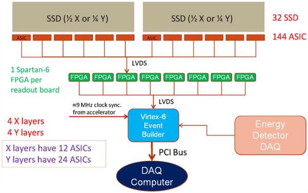
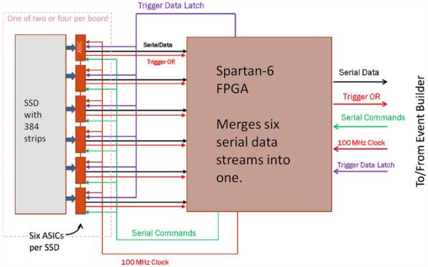
Fig. 1 gives an overview of the pCT tracker data acquisition system within which the ASIC will operate. A pair of x, y tracking layers precedes the subject to be imaged, and a second pair follows, to provide measurements of the entering and exiting proton trajectories. Twelve dozen ASICs are needed, and each of eight FPGAs handles the data flow, as well as control, of 12 or 24 ASICs. To achieve the necessary event readout rate, each ASIC has a dedicated serial data path to an FPGA. The FPGAs are mounted on the same printed circuit boards as the ASICs, as indicated in Fig. 2, resulting in a very compact readout system. Each tracker board has a dedicated output serial link connecting it to the event builder. All of the serial communication is made via LVDS, and 100 megabits per second is adequate speed, as demonstrated by simulations in Section VIII.
Fig. 1.
Overview of the planned pCT data acquisition.
Fig. 2.
Simplified block diagram of a tracker readout board. Only six of the 12 or 24 ASICs are shown here.
The readout is triggered, by the energy detector and tracker, for ease of synchronization and event building, with ample buffering at the front end to minimize dead time. The events of interest produce sparse data. With only a single proton passing through the tracker, an event data packet flowing from a single front-end board to the event builder FPGA will typically consist of a single cluster (noise hits will be rare and contribute negligibly to the data volume). Therefore, 100 Mbit/s capability on those data links is sufficient as long as the ASIC is able to zero-suppress its data and format it into a cluster list for output. The final link of an event to the computer will need to handle almost 1 Gbit/s, so the event builder will be installed onto the computer’s PCI bus, giving it direct access to the computer’s memory. Alternatively, fast Ethernet may be used to send the data to the computer.
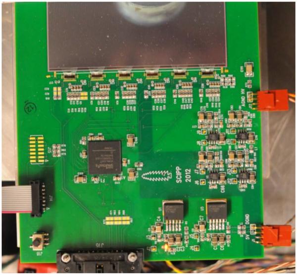
Although this data acquisition system is still under construction, we already have two fully functional test boards, each of which includes a single SSD, six ASICs, and the Spartan-6 FPGA (see Fig. 6). Those boards were used to obtain the ASIC test results presented here.
Fig. 6.
Photograph of one of the two ASIC test boards. The board is 13 cm wide.
III. FRONT-END ASIC
Our existing prototype pCT instrument is based on front-end ASICs designed by one of us (Johnson) for the Fermi-LAT gamma-ray telescope [9], which has been operating flawlessly in orbit since June of 2008. That in turn was based on earlier work on the ASIC for the silicon vertex tracker (SVT) of the BaBar experiment of the SLAC B-Factory [10]. All of these systems discriminate the signal in the front-end chip using a single threshold. That is a simple technique that we have found to give outstanding performance in tracking systems, for which recording of the pulse amplitude adds little to the capability but a lot to the system complexity. The BaBar SVT ASIC also recorded the time over threshold per channel for use in particle identification, and the Fermi-LAT ASICs recorded the time-over-threshold of the trigger signal (an OR of all discriminator outputs in a layer), to aid in background rejection. In contrast, the pCT ASIC does not record the time over threshold, in order to achieve the necessary throughput (although by altering the configuration settings, a time-over-threshold measurement of the trigger signal can be made in the FPGA for diagnostic purposes).
The Fermi-LAT system design, with nearly 900,000 tracker channels, emphasized low power and was intended to trigger at rates of a few kHz, using amplifiers with a two microsecond peaking time. It operates with very low noise occupancy: after masking a small percentage of noisy SSD strips there is less than one noise hit per trigger in the entire system. And the efficiency for detecting a minimum ionizing particle passing through a single active layer is greater than 99.5%. A notable drawback of the system, however, is that a hit from a cosmic ray has about an 8 to 10 microsecond window in which to be included in a trigger, resulting in a significant number of gamma-ray events that include a troublesome out-of-time cosmic-ray “ghost” track. That could have been alleviated by including extra digital logic per channel to define a narrower time window, something that is essential in the corresponding pCT design, as described below.
The new ASIC design, optimized for pCT, builds upon the Fermi-LAT experience but differs in several important aspects, mostly related to speed.
The common features are
64 channels, with a low-noise charge-to-voltage (current integrating) amplifier and a discriminator on each channel. The amplifiers are always live, acquiring data at all times, in particular during event readout.
Buffering of up to four events, to transform the stochastic event arrival time into a smooth output data flow, thus minimizing dead time.
An internal calibration system that allows an arbitrary set of channels to be pulsed with an externally specified input charge.
A threshold that is common to the 64 channels but can be set differently for each chip by external command.
An asynchronous output pulse that is the logical-OR of all channels, to be used as a trigger input (the Fermi-LAT tracking system is self triggering [11]).
Programmable mask registers that can decouple individual channels from the trigger and/or data flow.
A command interpreter that allows each IC to be individually configured by external digital commands.
Serial LVDS input/output.
The following features have been incorporated into the new design to enhance the capability for pCT:
Faster integration and CR-RC pulse shaping (differentiator followed by a single integrator), with a selection between 200 ns versus 400 ns peaking times.
Polarity selection, so that the chip can work with either sign of the input current (e.g., on both sides of a double-sided silicon-strip detector).
High and low gain selection (60 mV/fC and 15 mV/fC), to optimize the readout dynamic range for the higher ionization of protons exiting versus entering the subject.
A digital one-shot on each channel, to detect the rising edge from the discriminator and output a short pulse of fixed (programmable) length, followed by a 32-sample-deep storage pipeline (implemented in RAM) to hold the pulses pending a trigger decision. This is to ensure that protons in separate beam pulses will be kept separate in the data stream.
Four parallel event processors that reduce the 64-bit channel hit list down to a serial-encoded cluster list, suppressing data from all channels without signals (zero suppression). The output stream specifies the starting channel of each cluster and the cluster length.
A separate 100 Mbit/s output serial link per chip (the Fermi-LAT design daisy-chained the readout of 24 chips and operated at 20 Mbit/s).
The pCT ASIC was manufactured in the TSMC 250 nm mixed-mode process (CM025 [12]), with the first chips received in September 2012. The analog circuitry runs at 3.3 V and 2.1 V, using 1.3 mW of power per channel. The digital circuitry runs at 2.5 V and uses 2.3 mW per channel at 100 MHz.
IV. ASIC FUNCTIONALITY
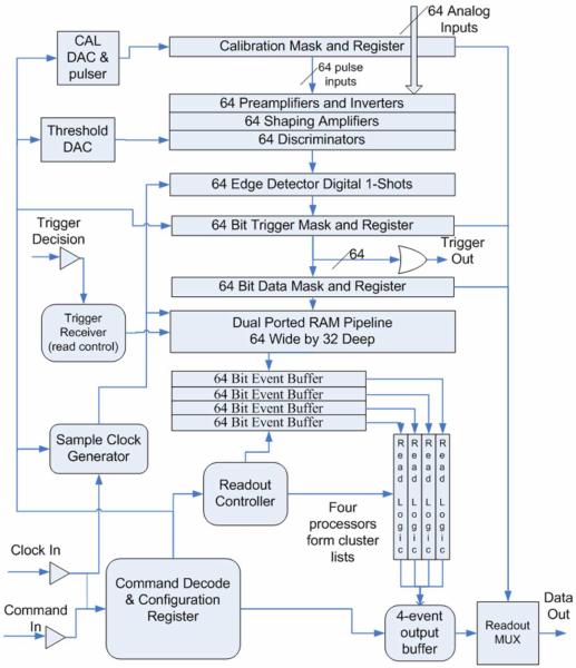
Fig. 3 gives an overview of the contents of the ASIC. The input stage is a charge sensitive preamplifier that is optionally followed by an inverter, which can be switched in or out of the circuit depending on the expected sign of the input signal. That stage is then AC coupled to an CR-RC shaping amplifier, which in turn is DC coupled to a comparator that serves as the discriminator, with the threshold set by loading the eight-bit threshold DAC register.
Fig. 3.
Simplified block diagram of the ASIC.
The discriminator output is high as long as the shaping amplifier output is above threshold, which could be a microsecond or longer, depending on the amount of charge deposited. But two successive triggers can occur as little as 110 ns apart in our application. Therefore, the comparator output is passed through a small clock-synchronous state machine (“digital 1-shot”) in each channel, which detects the comparator rising edge and outputs a pulse either two or three clock periods in length (depending on the configuration setting). The relevant clock is the “sample clock,” with a typical period of about 50 ns. It can be set, using three bits in the configuration register, to an integer multiple, ranging from 1 to 8, of the system clock period.
The data must be held pending a trigger decision. That is accomplished by a dual-port RAM pipeline that is 32 samples deep on each channel (i.e., for a maximum trigger latency of 1.6 microseconds with our typical clock setting). The write address circulates sequentially through the buffer at the rate of the sampling clock. The read address follows at a fixed offset set by five bits in the configuration register, which must be tuned to match the constant delay of the trigger. The trigger decision is transmitted to the chip on a dedicated line, so as not to interfere with read commands. It consists of a serial stream of three bits: a start bit followed by the two-bit address of the event buffer to be used. Once the three bits have been received and decoded, the RAM data pointed to by the read address are moved into the specified 64-bit event buffer. Note that depending on the set-up of the 1-shot, a hit in the data will occupy two or three successive addresses in the RAM, to accommodate trigger time jitter at the level of one or two periods of the sampling clock. Nevertheless, to optimize the timing of the data sampling (especially for the energy detector), we plan to phase lock the system clock to the accelerator RF.
As soon as the data are captured in the event buffer, they are then serially clocked into the corresponding event processor (one of four, which operate in parallel). The processor detects sets of contiguous hits, which form a “cluster,” and enters into the corresponding output buffer the starting strip of each cluster and its length. A minimum of 64 clock cycles is required for this process, but with four processors operating in parallel on a 100 MHz clock, the chip can easily keep up with a few megahertz trigger rate, as long as there are not too many clusters per event. In principle there could be up to 32 clusters in the event buffer (if every other strip were hit), but the output buffer can hold only ten. Once that limit is reached the remainder of the event is ignored. In fact, the upper limit can be lowered, if necessary, by setting four bits in the configuration register. Note that in the pCT system it will be rare to have more than one cluster from a chip in a given event.
The data remain in the output buffer until the chip receives a read command, which specifies in its data field the two-bit buffer address. The data, including a parity bit, then are output serially at 100 Mbit/s. If the output is busy with another event from a different buffer, the read command is buffered internally. Therefore, it can be sent at any time following the corresponding trigger.
If a trigger is received when all event output buffers are full, then an error is generated, setting the corresponding bit in the configuration register. Similarly, a read command received prior to the corresponding trigger will set an error bit. A parity error in a command will set a third error bit. The header in an output event stream indicates whether there is an error bit set, and the bits can be reviewed by reading back the configuration register. In our data acquisition (DAQ) system, the FPGA firmware is responsible for managing the buffers and holding the trigger dead when all buffers are full.
Using the internal calibration system, any subset of channels can be pulsed with a selected amount of charge. The calibration command not only initiates the pulse, it also delivers a trigger signal after a delay specified in the command’s data field. The channels to be pulsed are selected by loading the 64-bit calibration mask register, and the amount of charge is selected by loading the eight bit calibration DAC register. The charge is injected by a voltage step applied to a 25 fF capacitor. The sign of the voltage step is inverted when the configuration of the amplifiers is set up to engage the inverter between the preamplifier and shaping amplifier.
Another 64-bit register is used to mask noisy channels (typically caused by bad detector strips), so that they do not contribute to the data stream. Yet another is used to mask noisy channels from contributing to the trigger output, which is simply a logical OR of all unmasked channels. Normally the input to the OR is the output of the digital 1-shots, but by setting a bit in the configuration register it can be taken instead from the comparator outputs. That can be useful for diagnostic purposes, as the time-over-threshold is then given by the length of the trigger pulse.
The contents of all six of the registers can be viewed by means of non-destructive reads, with the bits sent out on the serial data output line. There are 15 commands for setting up and controlling the chip: reset, read data, calibration pulse, six register load commands, and six register read commands. Each command includes a five-bit address to select the chip, where the chip’s address is set by five wire-bond pads. If all five bits in the address field are set, then all chips will respond.
All of the chip’s digital I/O is LVDS, which is essential in an SSD system, to avoid digital interference with the sensitive amplifiers. Two bits in the configuration register are used to select among four settings for the output LVDS current drive.
V. ANALOG DESIGN
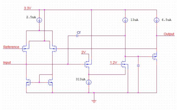
The charge sensitive preamplifier consists of a folded-cas-code amplifier followed by a source-follower output driver, as illustrated in Fig. 4. The input transistor is p-channel, with its source fed from a two-volt supply and its n-well biased at 3.3 volts. Its channel length is 0.7 micrometers, with a width of 3.675 mm and a nominal bias current of 300 microamperes. The feedback capacitance and the capacitance on the output of the cascode amplifier are composed of several capacitors in parallel, with individual capacitors switched in or out of the circuit according to the gain, polarity, and time-constant settings in the configuration register.
Fig. 4.
Simplified schematic of the preamplifier.
The DC feedback occurs via a weak differential amplifier that restores the output baseline to a voltage set by the “reference,” which in turn depends on the polarity setting. Using a different reference voltage for each of the polarity settings allows us to maximize the dynamic range for both.
The recovery time of the preamplifier normally is long compared with the expected average interval between proton triggers. If the protons were always to hit the same strip in each layer, then pileup would quickly saturate the preamplifier dynamic range. In our application that will not happen, as the beam spot is expected to cover all 768 or 1536 strips in each layer. Some pileup can be accommodated in case a strip is by chance hit multiple times in a short time interval, especially if the low gain setting is used where slow protons are expected. For example, in the low gain setting, simulations predict that at least ten signals from 10 MeV protons can pile up before saturation occurs.
But if instead a pencil beam were used in a raster scan, then some care should be taken to avoid excessive pileup. For example, in [13] the 19 mm FWHM spot size would cover about 80 strips, in which case for a 2 MHz proton rate the amplifier would need to recover fully in less than about 40 microseconds, close to the Spice-simulated recovery time given by the amplifier settings that we are using. The raster-scan beams of up to 35 mm FWHM advocated in [14] would be well suited to this system. But smaller spot sizes could be accommodated, since the amplifier recovery time can be adjusted over a wide range by changing one of five external resistors that provide reference currents for the chip. Using a very short recovery time would adversely affect the gain and noise performance, but as shown below, the system has a lot of noise margin to work with.
The preamplifier output is DC coupled to an inverting stage, which is intended to be enabled only for negative signals, by setting the appropriate bit in the configuration register. It consists of a simple common-source amplifier that has a voltage gain close to negative unity, followed by a source follower. For positive input signals the chip is to be configured to bypass the inverter stage. In either case, the output is AC coupled to the shaping amplifier.
The shaping amplifier is a cascode inverting amplifier with an n-channel input transistor, followed by a source follower. It is similar to the preamplifier, except that the cascode amplifier is not folded and carries a current of only six microamperes. The AC coupling capacitance, the feedback capacitance, and the capacitance on the output node of the cascode amplifier are all composed of multiple capacitors switched in or out of the circuit in order to adjust the gain and integration time constant according to the various configurations.
The DC feedback of the shaping amplifier looks the same as that of the preamplifier, except that its differential amplifier carries a larger current in order to produce a differentiation time constant roughly equal to the integration time constant, both of which are set according to the two time-constant choices in the configuration register. The differential amplifier in the feedback serves to hold the amplifier output baseline at 0.8 volts. The stability of this baseline is crucial, as the shaping amplifier output is DC coupled to the following comparator stage. Good matching of the transistor pairs in this differential amplifier, as well as those in the comparator, is critical for equalizing the thresholds across the 64 channels.
The comparator stage is a conventional two-stage differential amplifier followed by two digital inverters. The p-channel input transistors are 0.7 micrometers in length and 26 micrometers in width, with a tail current of 17.5 microamperes. A 10 fF capacitor provides a small amount of positive feedback. The comparator is driven by the source-follower output stage of the shaping amplifier, which carries a 35 microampere current.
The two DACs, one for the calibration amplitude and the other for the threshold setting, have seven bit resolution, with an eight bit used to select a high or low range. Each has a differential amplifier that copies the external 1.2 V LVDS reference voltage and uses it to generate a 1 or 5 microampere current, corresponding to the low or high range, across a polysilicon resistor. The current is copied by seven p-channel cascode current mirrors, each a factor of two higher in current than the previous and turned on or off by a CMOS switch, to establish the binary current setting. There is no need for speed. A few hundred microseconds are needed following a change in the setting to allow all of the analog circuits to settle.
In the case of the threshold DAC, the summed current passes through a resistor and then an n-channel transistor. A differential amplifier with negative feedback keeps the voltage across the transistor at a constant value close to 0.8 V, irrespective of the current. That establishes the reference voltage for the shaping amplifier outputs, whereas the voltage across the resistor sets the discriminator thresholds.
VI. CHIP LAYOUT
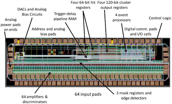
The overall chip layout can be seen in Fig. 5. The design is full-custom, using five metal layers, and incorporates no outside intellectual property. The digital layout is based upon a small set of custom cells that were conservatively designed, since silicon area and power consumption were not important design drivers. The digital and analog sections are well isolated in the design, with separate ground pads. Of course, both grounds contact the substrate and are connected together on the printed circuit board. We have found that the digital activity does not affect the analog amplifiers noticeably as long as the clocking activity is continuous. There are no gated clocks in the design. All flip flops are clocked continuously, keeping the current flowing into the digital ground relatively constant.
Fig. 5.
Layout of the pCT tracker ASIC, 6.0 mm by 1.8 mm in size.
The bias current for the front-end transistors, the currents for the differential amplifiers in the DC feedback circuits of the preamplifier and shaping amplifier, the reference current used to generate all other amplifier and comparator currents, and the LVDS driver reference current all are set by five separate external resistors, requiring five dedicated wire-bond pads. That was done to ensure that we would be able to adjust the amplifier performance as needed in case that the circuits did not behave as simulated. So far that conservatism has turned out not to have been necessary, but it would allow the chip to be optimized for other applications.
VII. ASIC TEST RESULTS
The ASIC from the initial fabrication run is fully functional and suitable for operation in the pCT system, with excellent noise and channel-matching performance. It operates continuously in our lab at a 100 MHz clock rate, detecting signals from minimum-ionizing beta-decay electrons and cosmic-ray muons, with no observable digital interference of the charge-sensitive amplifiers. The testing was done using two test boards, one of which is pictured in Fig. 6. Forty-two channels of each of six ASICs are directly wire bonded to the SSD at the top of the photograph (in the final assembly there will be a pitch-adapter circuit in between, to allow all 64 channels to be connected). A Spartan-6 FPGA interfaces the ASICs to the data acquisition system via the 20-pin header. The six linear voltage regulator chips supply power to the ASICs and the FPGA.
Yield data are limited thus far, as only thirteen chips have been tested. But of those thirteen chips, all tested 100% functional, including all 64 analog channels in each, suggesting a very good yield. For all of the chips tested, the gains and time constants were consistent with what we expected from the simulations. The external resistors used to set the currents were chosen based on simulations and have never been changed.
In contrast to the Fermi-LAT ASIC, for which power consumption was of paramount importance, for this design it was a minor consideration. Since all of the currents are set by external resistors, the analog power could be lowered significantly, with some loss of low-noise performance. But at a 100 MHz clock rate, the digital power dominates anyway. As operated in all of the tests presented here, the analog circuitry consumed 1.3 mW per channel, whereas the digital circuitry consumed 2.3 mW per channel, including the I/O circuits operating with their LVDS output drivers set to their maximum current of 3 mA.
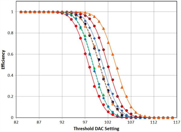
The chip’s channel-to-channel threshold uniformity was measured by using the internal calibration system to inject charge into selected channels while scanning the threshold across the transition from 100% efficiency to 0%. The efficiency curves were fit to complementary error functions (erfc), from which the gain and noise sigma were determined. See Fig. 7 for some example scans. From the six chips on the board shown in Fig. 6, we found that channels connected to 9 cm detector strips had on average only 0.08% lower gain than unconnected channels.
Fig. 7.
Threshold scans made on eight adjacent channels connected to 18 cm long detector strips, using one thousand 6.4 fC pulses per point, injected by the internal calibration system. The smooth curves represent fits of the complimentary error function to the data.
The measured threshold uniformity within a chip was excellent. For an average chip, the rms variation across the disconnected channels was 1.8%, rising to 2.1% for the connected channels. That means that all 64 channel thresholds may be set by a single DAC with no compromise of the efficiency or noise performance. The observed threshold variation includes contributions from gain variations, shaping amplifier output baseline variations, comparator input offsets, and variations in the calibration capacitors. The rms variation from one chip to the next is expected to be larger. It is observed to be about 5.4%, based on measurements made across the six chips on a single test board.
We measured the amplifier noise for the 200 ns peaking-time setting from the same threshold scans. The measurements were done using the board in Fig. 6, using the disconnected channels as well as the channels connected to a single detector 9-cm strip (~11 pF). Measurements were also done on another board with two 8-strip detectors connected in series, to give 18-cm long strips. The threshold curves for those eight long strips are all shown in Fig. 7. The measurements are summarized by an rms equivalent noise charge, averaged over channels, of
| (1) |
with C in picofarads. For the longest strips in our pCT system, 18 cm (~22 pF), this corresponds to 1050 electrons (0.17 fC) ENC, compared to the 60,000 electron (9.5 fC) most-probable signal from 250 MeV protons. This noise performance is better than needed for our pCT system, but the chip was designed also to work with thinner detectors and longer strips in a larger, more advanced system.1
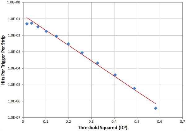
A more direct indicator of the noise performance comes from looking at the noise occupancy, measured by taking a million randomly timed triggers for each threshold setting, with 18 cm strips connected to the channels. The results are shown in Fig. 8. Clearly we have a wide range over which to choose a threshold setting that will guarantee 100% efficiency for protons with zero hits from electronics noise.
Fig. 8.
The noise occupancy measured from eight adjacent channels connected to 18 cm strips (~22 pF). Each point was measured from a million randomly timed triggers, each with a 150 ns window (a parameter that is adjustable on the chip). Note that the most probable signal from a 250 MeV proton is 9.5 fC. From the slope of the displayed linear fit we find a noise sigma of 960 electrons, consistent with the fits shown in Fig. 7.
An estimate of the noise sigma can also be extracted from Fig. 8 by observing that for Gaussian noise the rate should fall exponentially with the increasing square of the threshold (considering the asymptotic form of the erfc function). From the slope of the linear fit displayed in the figure we find
| (2) |
Our demonstrated excellent ASIC signal-to-noise performance offers multiple important advantages to the pCT system. Only beam-related particles will make hits in the detectors, so there will be no electronic-noise hits present to confuse pattern recognition and increase the data volume. Furthermore, even the smallest proton signals will be far above threshold, thus minimizing time jitter of the threshold crossings and ensuring that all hits can be captured within the planned 110 ns window with efficiency very close to 100%. This is crucial, as the loss of even a single proton hit due to non-localized inefficiencies would make the event unusable for CT. The 100% hit efficiency will also allow us to treat the small (1/2 mm) gaps between detectors that are parallel to the strips, as well as possible isolated dead detector strips, in a simple way. A missing hit in a single layer will indicate that the proton passed through such a gap, thus localizing it nearly as well as is accomplished by a hit strip.
VIII. DAQ SIMULATIONS
We have not yet operated in beam tests the data acquisition system for which these chips are intended, and our laboratory particle sources do not have anywhere near the intensity needed to test the system at its design trigger rate. But based on the excellent ASIC test results, in particular the negligible noise occupancy, together with Verilog simulations of the tracker data acquisition system, we have made reliable predictions of the system performance. The Verilog simulations were based on the schematic-extracted netlist of the ASIC, together with prototype data-acquisition code designed to run on the tracker-board FPGA (and already demonstrated to work on the test board).
The 9.1-MHz LLUMC proton-accelerator beam structure was simulated with a Poisson-distributed number of protons per beam pulse, for a total proton rate of 1.97 million per second, with at least one proton in each of 19% of the beam pulses. The detectors were simulated with hits distributed uniformly across the active area, with one or two strips per cluster. Random noise hits were conservatively added at an occupancy of 10−4 per strip per trigger. The ASICs and the data acquisition were simulated with a 91 MHz clock and 91 Mbps LVDS data transfer rates from ASIC to FPGA and from FPGA to event builder.
The resulting dead-time fraction was only 2.3%, with the front-end buffers occupied as shown in Table I. That yielded a rate for recorded events of 1.54 MHz, of which 10.6% had more than one proton, and therefore would not be usable, because the energy detector could not distinguish between the protons. Evidently the LLUMC accelerator beam structure is the limiting factor in the achievable data rate. A 91 MHz DAQ clock rate is more than sufficient to avoid significant contributions to the dead time by the DAQ system.
TABLE I.
SIMULATED BUFFER OCCUPANCY
| Number of Buffers Occupied | Fraction of Triggers |
|---|---|
| 0 | 10.7% |
| 1 | 34.2% |
| 2 | 29.2% |
| 3 | 20.7% |
| 4 | 2.3% |
IX. CONCLUSION
We have developed and tested an ASIC around which we can build a silicon-strip based tracking system for proton computed tomography that will accurately track at least a million protons per second. The chip can be used for single-side or double sided AC-coupled detectors, and it includes a wide range of configuration settings that could make it suitable for other similar applications. Its noise performance is good enough for it to operate with zero electronic-noise occupancy, even with significantly thinner and larger detectors than what we are using in our clinical prototype pCT scanner.
ACKNOWLEDGMENT
This work was supported in part by the National Institute of Biomedical Imaging and Bioengineering (NIBIB) and the NSF, Award R01EB013118.
The authors thank the Xilinx Corporation for donating the Virtex-6 FPGA evaluation boards and associated programming hardware and software. They acknowledge support from their technical staff at UCSC, especially Serguei Kachiguine, Forest McKinney, and Max Wilder, and from their other colleagues in their pCT collaboration: Tia Plautz and Andriy Zatserklyaniy at UCSC, V. Bashkirov, F. Hurley, and R. Schulte at the Loma Linda University Medical Center, CA 92354, and K. Schubert, B. Schultze, and M. Witt at CSU San Bernardino, San Bernardino, CA 92407 USA. The content of this paper is solely the responsibility of the authors and does not necessarily represent the official views of NIBIB and NIH.
Footnotes
Color versions of one or more of the figures in this paper are available online at http://ieeexplore.ieee.org.
The detectors in use for our prototype system were left over from the Fermi-LAT project. Their thickness and strip pitch were optimized for that system.
REFERENCES
- 1.Sadrozinski HF-W, et al. Toward proton computed tomography. IEEE Trans. Nucl. Sci. 2004 Feb;51(1):3–9. doi: 10.1109/TNS.2013.2274663. [DOI] [PMC free article] [PubMed] [Google Scholar]
- 2.Wilson RR. Radiological use of fast protons. Radiology. 1946;47:487–491. doi: 10.1148/47.5.487. [DOI] [PubMed] [Google Scholar]
- 3.Cirrone GAP, et al. The Italian project for a proton imaging device. Nucl. Instrum. Methods Phys. Res. A. 2007;576(1):194–197. [Google Scholar]
- 4.Sadrozinski HF-W, et al. Development of a head scanner for proton CT. Nucl Instrum. Methods Phys. Res. A. 2013;699:205–210. doi: 10.1016/j.nima.2012.04.029. [DOI] [PMC free article] [PubMed] [Google Scholar]
- 5.Coutrakon G, Hubbard J, Johanning J, Maudsley G, Slaton T, Morton P. A performance study of the Loma Linda proton medical accelerator. Med. Phys. 1994;21(11):1691–1701. doi: 10.1118/1.597270. [DOI] [PubMed] [Google Scholar]
- 6.Atwood WB, et al. The large area telescope on the Fermi Gamma-ray space telescope mission. Astrophys. J. 2009;697:1071–1102. [Google Scholar]
- 7.The ATLAS experiment at the CERN large hadron collider. J. Instrum. 2008;3:S08003. ATLAS Collaboration. [Google Scholar]
- 8.The CMS experiment at the CERN large hadron collider. J. Instrum. 2008;3:S08004. CMS Collaboration. [Google Scholar]
- 9.Baldini L, et al. The silicon tracker readout electronics of the Gamma-Ray large area space telescope. IEEE Trans. Nucl. Sci. 2006 Apr;53(2):466–473. [Google Scholar]
- 10.Kipnis I, et al. A time-over-threshold machine: The readout integrated circuit for the babar silicon vertex tracker. IEEE Trans. Nucl. Sci. 1997 Jun;44(3):289–297. [Google Scholar]
- 11.Atwood W, et al. Design and initial tests of the tracker-converter of the gamma-ray large area space telescope. Astropart. Phys. 2007;28(2):422–434. [Google Scholar]
- 12.See the MOSIS Service at the University of Southern California. [Online]. Available: http://www.mosis.com/vendors/view/tsmc/025.
- 13.Lomax AJ, et al. Treatment planning and verification of proton therapy using spot scanning: Initial experiences. Med. Phys. 2004;31:3150–3157. doi: 10.1118/1.1779371. [DOI] [PubMed] [Google Scholar]
- 14.Kooy HM, et al. A case study in proton pencil-beam scanning delivery. Int. J. Radiat. Oncol. Biol. Phys. 2010;76:624–630. doi: 10.1016/j.ijrobp.2009.06.065. [DOI] [PubMed] [Google Scholar]


