

Abstract
Nanowire nanoelectronic devices have been exploited as highly sensitive subcellular resolution detectors for recording extracellular and intracellular signals from cells, as well as from natural and engineered/cyborg tissues, and in this capacity open many opportunities for fundamental biological research and biomedical applications. Here we demonstrate the capability to take full advantage of the attractive capabilities of nanowire nanoelectronic devices for long term physiological studies by passivating the nanowire elements with ultrathin metal oxide shells. Studies of Si and Si/aluminum oxide (Al2O3) core/shell nanowires in physiological solutions at 37 °C demonstrate long-term stability extending for at least 100 days in samples coated with 10 nm thick Al2O3 shells. In addition, investigations of nanowires configured as field-effect transistors (FETs) demonstrate that the Si/Al2O3 core/shell nanowire FETs exhibit good device performance for at least 4 months in physiological model solutions at 37 °C. The generality of this approach was also tested with in studies of Ge/Si and InAs nanowires, where Ge/Si/Al2O3 and InAs/Al2O3 core/shell materials exhibited stability for at least 100 days in physiological model solutions at 37 °C. In addition, investigations of hafnium oxide-Al2O3 nanolaminated shells indicate the potential to extend nanowire stability well beyond 1 year time scale in vivo. These studies demonstrate that straightforward core/shell nanowire nanoelectronic devices can exhibit the long term stability needed for a range of chronic in vivo studies in animals as well as powerful biomedical implants that could improve monitoring and treatment of disease.
Keywords: Bioelectronics, nanosensor, field-effect transistor, silicon nanowire, Al2O3, atomic layer deposition
Nanoelectronic devices based on bottom-up synthesized nanowires have demonstrated unique capabilities for probing and interfacing to biological systems with high sensitivity and spatial-temporal resolution.1−17 For example, silicon nanowire FETs have been used for real-time in vitro detection of disease markers proteins and even single virus particles,5−9 recording extracellular action potentials from cells and acute brain tissue slices with subcellular spatial resolution,10−13 recording intracellular action potentials from beating cardiac cells,14−16 and the development of electronically innervated three-dimensional cyborg tissues.17 Some of the directions being pursued with nanowire nanoelectronic devices, such as in vitro sensing, do not require long-term stability and biocompatibility, yet applications focused on chronic in vivo cell-recording, implantable cyborg tissues, and more general implantable devices do require long-term nanowire stability in physiological environments.
Previous studies of cultured neurons with silicon nanowire devices10,17 have demonstrated functional stability on at least a 2–3 week time scale, although other work18 has reported dissolution of nanoscale silicon under physiological conditions on a shorter times. Taking silicon nanowires as a prototypical nanoelectronic system, it is interesting to consider possible degradation pathways as well as methods for stabilization. Silicon nanowires and FETs will have a native SiO2 surface passivation layer under standard fabrication conditions due to oxidation in air.19 The SiO2 layer is stable in the dry state but can dissolve by hydrolysis in aqueous solutions20,21 with a rate accelerated at higher ionic strengths typical of physiological environments.22,23 Dissolution of silicon structures can occur by a cycle in which the silicon surface is reoxidized and dissolved. The fact that previous studies have reported different stabilities10,17,18 may reflect the complexity of inorganic nanostructure/cell interfaces where protein adsorption24 and/or lowered oxygen concentrations could substantially slow dissolution steps.
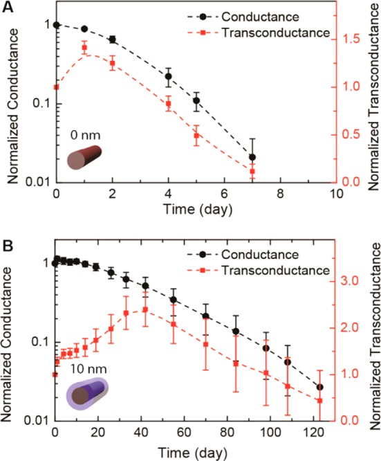
Hence, it should be straightforward to enhance the stability of silicon (or silica) and other nanowires in a rational manner by introducing a stable conformal shell material. Here we demonstrate this concept for improving the intrinsic long-term stability of nanowire nanoelectronics in physiological environments using a core/shell architecture, where the shell is a metal-oxide such as Al2O3. Our overall experimental strategy (Figure 1A) involves direct comparison of the stability of Si and Si/Al2O3 core/shell nanowires alone or configured as FET devices in biologically relevant solutions at 37 °C and room temperature. Al2O3 was chosen as the nanowire shell material in the majority of our studies for several reasons. First, Al2O3 has excellent chemical stability in the physiological environments, and moreover, has been explored as a material for implanted dental and orthopedic applications.25,26 Second, the Al2O3 shells should not adversely affect the performance of nanowire FETs since Al2O3 is a high dielectric constant gate material.27 Third, it is easy to achieve high-quality, pinhole free, conformal shells of Al2O3 on nanowires with accurate control of thickness in the nanometer scale by atomic layer deposition (ALD) technique.28,29
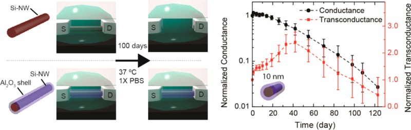
Figure 1.
Core/shell stabilization of nanowire devices in physiological environments. (A) Schematic illustration of long-time evolution of Si-nanowire FET devices with and without Al2O3 protective shell in physiological mimicking 1× PBS (pH 7.4) at 37 °C. TEM images of (B) a Si nanowire with native surface oxide, and (C) a Si nanowire with a 5 nm thick Al2O3 shell. The Al2O3 was annealed at 400 °C for 1 min prior to sample preparation.
The Si nanowires (30 nm diameter) were grown by our previously reported gold nanoparticle catalyzed vapor–liquid–solid (VLS) method.30−32 Calibrated thickness Al2O3 shells were deposited on the Si nanowires by ALD at 150 °C and then annealed (1 min, rapid thermal annealing (RTA)) at 400 °C.33 A transmission electron microcopy (TEM) image of a representative Si nanowire (Figure 1B) reveals a typical <0.5 nm thick amorphous layer on the surface, which can be attributed to the silicon oxide,19 and a crystalline Si structure for the nanowire core. In contrast, a TEM image of a Si/Al2O3 core/shell nanowire (Figure 1C) shows a uniform 5–6 nm thick amorphous Al2O3 shell on a crystalline Si nanowire core. The thickness of the shell is consistent with that expected for the 50 ALD cycles used for deposition, and moreover, the amorphous structure post 400 °C/1 min RTA is consistent with previous studies showing that >650 °C temperatures are required to initiate the crystallization of amorphous Al2O3.34
We initially investigated the stability of Si and Si/Al2O3 core/shell nanowire under different aqueous solution conditions using the method shown schematically in Figure 2A.35 In brief, we patterned 4 μm pitch photoresist stripes on the nanowires so that only regions not covered by photoresist were exposed to solutions (Supporting Information, Figure S1). Samples were immersed in either 1× PBS (pH 7.4) or 1× Neurobasal solutions36 (pH 7.3) at either 37 °C in an incubator or at a room temperature for fixed time periods, and after removal from solution the photoresist was removed and the nanowire substrates were imaged by dark-field optical microscopy. Dark-field imaging provides a sensitive assessment of dissolution since the Rayleigh scattering intensity depends on nanowire diameter to sixth power (i.e., Iscattering ∝ d6) on the nanometer scale.37
Figure 2.

Nanowire stability in solution. (A) Schematic illustrating the experiment methodology. (B–D) Dark-field microscope images showing morphology evolution of Si nanowires with different Al2O3 shell thickness in (B) 1× PBS at 37 °C, (C) 1× PBS at room temperature, and (D) Neurobasal at 37 °C.
Dark-field images recorded from Si nanowire samples have 0, 5, and 10 nm Al2O3 shell thicknesses following immersion in 1× PBS at 37 °C 10, 50, and 100 days (Figure 2B) show several key features. First, Si nanowires without Al2O3 shells exhibited dissolution in the nanowire regions not protected by photoresist after 10 days, although the nanowire structures remain continuous. Second, Si nanowire samples exposed for 50 or 100 days showed complete dissolution of the Si in regions exposed to solution and not protected by photoresist. In contrast, the Si nanowires with 5 and 10 nm thick Al2O3 shells, where all Al2O3 shells were annealed for 1 min at 400 °C, exhibited substantially greater stability in 1× PBS at 37 °C. For example, Si nanowires with 5 nm shells showed little dissolution at 50 days, and nanowires with 10 nm shells were similar at 100 days.
In addition, we have investigated stability of these different core/shell Si nanowires at room temperature since many sensing and diagnostic applications nanowire FET detectors are carried out under ambient conditions. Dark-field images recorded from similar Si nanowire samples having 0, 5, and 10 nm Al2O3 shell following immersion in 1× PBS at room temperature (Figure 2C) showed substantially greater stability. For example, the Si nanowires without Al2O3 shells do not show obvious signs of dissolution until ca. 40–50 days and are still continuous structures at this point. This corresponds to ∼4–5 times slower rate and is consistent with expectations for an activated process (at lower temperatures). Moreover, the Si/Al2O3 core/shell nanowires with 5 and 10 nm shell thicknesses did not show any obvious dissolution after even 100 days in solution.
We also carried out stability studies in 1× Neurobasal neuron cell culture media36 as a closer analog (than PBS) to in vivo environments, where this medium contains amino acids and other organic components in addition to inorganic ions.36 Dark-field images recorded at different times from nanowire samples having 0, 5, and 10 nm Al2O3 thick shell following immersion in this medium at 37 °C (Figure 2D) show similar behavior as 1× PBS at 37 °C. The comparable dissolution behavior for the two media is consistent with their similar ionic strength and pH values. Significantly, these studies show the Si/Al2O3 core/shell nanowires with 10 nm thick shells remain stable for at least 100 days in both media at 37 °C.
To assess the long-term stability of nanowire bioelectronic sensor devices we fabricated FETs with Si and Si/Al2O3 core/shell nanowires and monitored the device characteristics when immersed in 1× PBS solutions at 37 °C for extended time periods. The source/drain contacts on the nanowires were fabricated using standard procedures and passivation with SU-8 photoresist.38 Device conductance and transconductance versus time data recorded39 for Si nanowires (Figure 3A) revealed several key features. First, the normalized average (N = 30) conductance decreased to less than 3% of the initial value at day 7. The transconductance initially exhibited an increase at day 1 but then decreased as observed for the conductance. However, the decrease in transconductance was much slower than conductance and at day 7 was still 13% of the initial value. For this reason, it is possible to utilize the Si nanowire FET devices until nearly the point of complete failure.
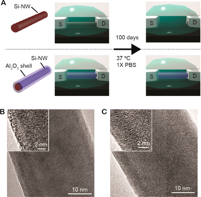
Figure 3.
Si and Si/Al2O3 nanowire FET devices stability in solution at 37 oC. Time-dependent evolution of the normalized conductance and transconductance for (A) Si nanowire and (B) Si/Al2O3 core/shell nanowire (10 nm thick shell) FET devices in 1× PBS at 37 °C. The averages were determined at solution gate voltage = 0 V from 30 devices in both (A) and (B).
Similar measurements carried out for Si/Al2O3 core/shell nanowire (10 nm thick shell) FET devices (Figure 3B) demonstrate long-term stability as expected based on our nanowire dissolution studies. Specifically, we found that the normalized average (N = 30) conductance of Si/Al2O3 nanowire FET devices was constant for ca. 20 days, and then decreased slowly until ca. 3% of the initial value at day 120. In addition, the normalized average transconductance of the Si/Al2O3 nanowire increased over during the first 50 days and then decreased to ca. 50% the initial value at day 120. These data demonstrate clearly that the Al2O3 shell can open chronic studies on a 4-month time-scale with functional nanowire nanoelectronic devices. Moreover, we believe that the observed changes in conductance and transconductance (Figure 3B) indicate that defects in the Al2O3 shells may play an important role in the device changes, and hence that efforts focus on improving the shell quality could further improve the nanowire stability. Indeed, preliminary studies of HfO2/Al2O3 nanolaminated shells show greatly enhanced endurance in accelerated tests in 10× PBS with stable structures expected for ca. 2 years.40
Last, we have explored the generality of Al2O3 shells to stabilize nanowires by exploring Ge/Si core/shell41−43 and InAs nanowires,44−46 which have been shown to exhibit higher hole and electron mobilities, respectively, than Si nanowires. Dark-field images recorded from Ge/Si and Ge/Si/Al2O3 nanowires (Figure 4a) as well as InAs and InAs/Al2O3 nanowires (Figure 4b) following immersion in 1× PBS at 37 °C for 10, 50, and 100 days show similar features to silicon nanowires described above. The Ge/Si and InAs nanowires exhibited relatively rapid dissolution with areas exposed to solution completed removed within 10 days at 37 °C. In contrast, our data show that the Al2O3 shells improve substantially the long-term stability to over 100 days for both Ge/Si and InAs nanowires. Therefore, by using this oxide shell strategy it is possible to extend the use of nonsilicon nanoelectronic devices to chronic biomedical applications in physiological conditions.
Figure 4.
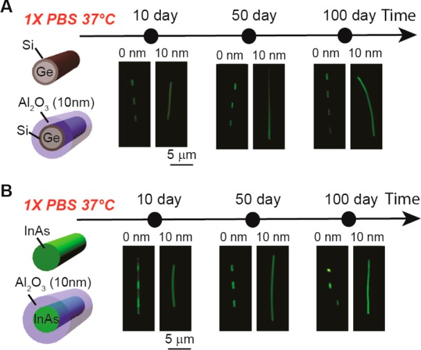
Stabilization of semiconductor nanowires with Al2O3 shells. Dark-field microscope images showing time-dependent evolution of (A) Ge/Si core/shell nanowires and (B) InAs nanowires with and without Al2O3 shells in 1× PBS at 37 °C.
In conclusion, we have demonstrated the capability to take full advantage of the attractive capabilities of nanowire nanoelectronic devices for long-term physiological studies by passivating the nanowire elements with ultrathin metal oxide shells. Studies of Si and Si/Al2O3 core/shell nanowires in physiological solutions at 37 °C show long-term stability extending for at least 100 days in samples with 10 nm thick Al2O3 shells. In addition, investigations of nanowires configured as field-effect transistors (FETs) demonstrate that the Si/Al2O3 core/shell nanowire FETs exhibit good device performance for at least 4 months in physiological model solutions at 37 °C. The generality of this approach was also tested with in studies of Ge/Si and InAs nanowires, where Ge/Si/Al2O3 and InAs/Al2O3 core/shell materials exhibited stability for at least 100 days in physiological model solutions at 37 °C. In addition, investigations of hafnium oxide/Al2O3 nanolaminate shells indicate the potential to extend nanowire stability well beyond 1 year time scale in vivo. These studies demonstrate that straightforward core/shell nanowire nanoelectronic devices can exhibit the long-term stability needed for a range of chronic in vivo studies in animals as well as powerful biomedical implants that could improve monitoring and treatment of disease.
Acknowledgments
This study was supported by National Institutes of Health Director’s Pioneer and National Security Science and Engineering Faculty Fellow awards (to C.M.L.).
Supporting Information Available
Additional information and figures. This material is available free of charge via the Internet at http://pubs.acs.org.
The authors declare no competing financial interest.
Author Contributions
§ These authors contributed equally to this work.
Funding Statement
National Institutes of Health, United States
Supplementary Material
References
- Patolsky F.; Zheng G. F.; Lieber C. M. Anal. Chem. 2006, 78, 4260–4269. [DOI] [PubMed] [Google Scholar]
- Patolsky F.; Timko B. P.; Zheng G. F.; Lieber C. M. MRS Bull. 2007, 32, 142–149. [Google Scholar]
- Kotov N. A.; Winter J. O.; Clements I. P.; Jan E.; Timko B. P.; Campidelli S.; Pathak S.; Mazzatenta A.; Lieber C. M.; Prato M.; Bellamkonda R. V.; Silva G. A.; Kam N. W. S.; Patolsky F.; Ballerini L. Adv. Mater. 2009, 21, 3970–4004. [Google Scholar]
- Chen K. I.; Li B. R.; Chen Y. T. Nano Today 2011, 6, 131–154. [Google Scholar]
- Cui Y.; Wei Q. Q.; Park H. K.; Lieber C. M. Science 2001, 293, 1289–1292. [DOI] [PubMed] [Google Scholar]
- Hahm J.; Lieber C. M. Nano Lett 2004, 4, 51–54. [Google Scholar]
- Patolsky F.; Zheng G. F.; Hayden O.; Lakadamyali M.; Zhuang X. W.; Lieber C. M. Proc. Natl. Acad. Sci. U.S.A. 2004, 101, 14017–14022. [DOI] [PMC free article] [PubMed] [Google Scholar]
- Wang W. U.; Chen C.; Lin K. H.; Fang Y.; Lieber C. M. Proc. Natl. Acad. Sci. U.S.A. 2005, 102, 3208–3212. [DOI] [PMC free article] [PubMed] [Google Scholar]
- Zheng G. F.; Patolsky F.; Cui Y.; Wang W. U.; Lieber C. M. Nat. Biotechnol. 2005, 23, 1294–1301. [DOI] [PubMed] [Google Scholar]
- Patolsky F.; Timko B. P.; Yu G. H.; Fang Y.; Greytak A. B.; Zheng G. F.; Lieber C. M. Science 2006, 313, 1100–1104. [DOI] [PubMed] [Google Scholar]
- Cohen-Karni T.; Timko B. P.; Weiss L. E.; Lieber C. M. Proc. Natl. Acad. Sci. U.S.A. 2009, 106, 7309–7313. [DOI] [PMC free article] [PubMed] [Google Scholar]
- Qing Q.; Pal S. K.; Tian B. Z.; Duan X. J.; Timko B. P.; Cohen-Karni T.; Murthy V. N.; Lieber C. M. Proc. Natl. Acad. Sci. U.S.A. 2010, 107, 1882–1887. [DOI] [PMC free article] [PubMed] [Google Scholar]
- Cohen-Karni T.; Casanova D.; Cahoon J. F.; Qing Q.; Bell D. C.; Lieber C. M. Nano Lett. 2012, 12, 2639–2644. [DOI] [PMC free article] [PubMed] [Google Scholar]
- Tian B. Z.; Cohen-Karni T.; Qing Q.; Duan X. J.; Xie P.; Lieber C. M. Science 2010, 329, 830–834. [DOI] [PMC free article] [PubMed] [Google Scholar]
- Duan X. J.; Gao R. X.; Xie P.; Cohen-Karni T.; Qing Q.; Choe H. S.; Tian B. Z.; Jiang X. C.; Lieber C. M. Nat. Nanotechnol. 2012, 7, 174–179. [DOI] [PMC free article] [PubMed] [Google Scholar]
- Qing Q.; JIang Z.; Xu L.; Mai L.; Lieber C. M. Nat. Nanotechnol. 2014, 10.1038/nnano.2013.273. [DOI] [PMC free article] [PubMed] [Google Scholar]
- Tian B. Z.; Liu J.; Dvir T.; Jin L. H.; Tsui J. H.; Qing Q.; Suo Z. G.; Langer R.; Kohane D. S.; Lieber C. M. Nat. Mater. 2012, 11, 986–994. [DOI] [PMC free article] [PubMed] [Google Scholar]
- Hwang S. W.; Tao H.; Kim D. H.; Cheng H. Y.; Song J. K.; Rill E.; Brenckle M. A.; Panilaitis B.; Won S. M.; Kim Y. S.; Song Y. M.; Yu K. J.; Ameen A.; Li R.; Su Y. W.; Yang M. M.; Kaplan D. L.; Zakin M. R.; Slepian M. J.; Huang Y. G.; Omenetto F. G.; Rogers J. A. Science 2012, 337, 1640–1644. [DOI] [PMC free article] [PubMed] [Google Scholar]
- Cui Y.; Lauhon L. J.; Gudiksen M. S.; Wang J. F.; Lieber C. M. Appl. Phys. Lett. 2001, 78, 2214–2216. [Google Scholar]
- Brady P. V.; Walther J. V. Chem. Geol. 1990, 82, 253–264. [Google Scholar]
- Rimstidt J. D.; Barnes H. L. Geochim. Cosmochim. Acta 1980, 44, 1683–1699. [Google Scholar]
- Ahn S.; Spuhler P. S.; Chiari M.; Cabodi M.; Unlu M. S. Biosens. Bioelectron. 2012, 36, 222–229. [DOI] [PubMed] [Google Scholar]
- Dove P. M.; Crerar D. A. Geochim. Cosmochim. Acta 1990, 54, 955–969. [Google Scholar]
- Lord M. S.; Foss M.; Besenbacher F. Nano Today 2010, 5, 66–78. [Google Scholar]
- Hench L. L. J. Am. Ceram. Soc. 1998, 81, 1705–1728. [Google Scholar]
- Ratner B. D.; Hoffman A. S.; Schoen F. J.; Lemons J. E.. Biomaterials Science - An Introduction to Materials in Medicine, 2nd ed.; Academic Press: New York, 2004. [Google Scholar]
- Robertson J. Eur. Phys. J.: Appl. Phys. 2004, 28, 265–291. [Google Scholar]
- Dillon A. C.; Ott A. W.; Way J. D.; George S. M. Surf. Sci. 1995, 322, 230–242. [Google Scholar]
- Groner M. D.; Fabreguette F. H.; Elam J. W.; George S. M. Chem. Mater. 2004, 16, 639–645. [Google Scholar]
- Morales A. M.; Lieber C. M. Science 1998, 279, 208–211. [DOI] [PubMed] [Google Scholar]
- Patolsky F.; Zheng G. F.; Lieber C. M. Nat. Protoc. 2006, 1, 1711–1724. [DOI] [PubMed] [Google Scholar]
- The Si nanowires were grown by a nanocluster-catalyzed vapor–liquid–solid growth method. Briefly, the growth substrate (600 nm SiO2/Si) was cleaned by oxygen plasma (50 W, 1 min), treated with poly-l-lysine solution (0.1%, Ted Pella) for 5 min, and then rinsed thoroughly with deionized water. For silicon nanowire synthesis, 30 nm gold nanoparticles (Ted Pella) were dispersed on growth substrates, and then nanowire growth was carried out at 450 °C under a constant pressure of 40 Torr with SiH4 (2.5 SCCM), diluted B2H6 (100 ppm in He, 3 SCCM), and H2 (60 SCCM) as reactant, doping, and carrier gases, respectively. The growth time was 30 min, producing an average nanowire length of 25 mm.
- Si nanowires on their respective growth substrates were placed in an ALD reactor (Savannah 200, Cambridge Nanotechnology Inc.), and Al2O3 shells were deposited using a standard protocol. Trimethylaluminum (TMA) and H2O were sequentially introduced into the ALD chamber with 0.015 s pulses with intervening 20 s N2 purging (20 SCCM) with the substrate temperature of 150 °C and a background pressure of 0.2 Torr. Fifty cycles were used for the deposition of ca. 5 nm of Al2O3 and 100 cycles for the deposition of ca. 10 nm of Al2O3. Postdeposition rapid thermal annealing at 400 °C for 1 min was used to improve the Al2O3 layers.
- Guha S.; Cartier E.; Bojarczuk N. A.; Bruley J.; Gignac L.; Karasinski J. J. Appl. Phys. 2001, 90, 512–514. [Google Scholar]
- Key steps used to test the long-term stability of Si, Ge/Si core/shell, and InAs nanowires are as follows: (1) Blank substrates (600 nm SiO2/Si) were coated with a 15 nm thick ALD-coated HfO2 film (150 cycle, 150 °C substrate temperature, and 1 min post rapid thermal annealing at 550 °C) to prevent etching of the SiO2 during studies. (2) Si, Ge/Si core/shell, or InAs nanowires with and without Al2O3 coatings were transferred to substrates by contact printing.5 (3) An ∼10 nm thick Cr film was deposited on nanowires to prevent etching of Al2O3 shells by the basic developer (Microposit MF CD 26) used during the photoresist patterning/developing process. (4) A 4 μm pitch periodic striped design was patterned by photolithography (Shipley 1805 photoresist), where regions of the photoresist crossing nanowires will be protected from solution. (5) The Cr metal in unprotected regions of the stripe design was removed with a Cr etchant (Cr-etchant 1020, Transene Inc.). (6) Following treatment in physiological electrolytes (e.g., in 1× PBS at 37 °C, and in Neurobasal at 37 °C) for a specific time duration, the patterned photoresist was removed using Remover PG (Microchem, Inc.), and then the Cr layer was removed as in step 5. (7) Nanowire/substrate samples were characterized using dark field microscopy.
- http://www.lifetechnologies.com/order/catalog/product/21103049 (accessed Feb 1, 2014).
- Hulst H. C.; Hulst H. C. v. d.. Light Scattering by Small Particles; Courier Dover Publications: Mineola, NY, 1957. [Google Scholar]
- Si-nanowire FET devices were fabricated as follows: (1) A 15 nm thick HfO2 film (150 cycle, 150 °C substrate temperature, and 1 min post rapid thermal annealing at 550 °C) was deposited by ALD on the surface of the substrate (600 nm SiO2/Si) (2) Si-nanowires were transferred directly from the growth wafer onto the HfO2 coated substrates by contact-printing. (3) Photolithography was used to define metal contacts/interconnects for an array of Si-nanowire FET devices. (4) After oxygen plasma treatment (50 W, 1 min) of the developed pattern to remove the photoresist residue, the SiO2 native oxide or Al2O3/native oxide was removed using buffered oxide etch (BOE, 1:7) for 7 or 25 s, respectively. (5) Cr/Pd (1.5/100 nm) were deposited by thermal evaporation to make interconnects and contacts to the Si-nanowire devices. (6) After lift-off, a 400 nm layer of SU-8 photoresist was spin-coated, prebaked at 95 °C for 5 min, and then patterned by photolithography to define a SU-8 passivation layer for the interconnects and contacts.
- Si-nanowire FET devices were immersed in 1× PBS (pH 7.4) at 37 °C in an incubator for time periods up to 120 days. At specific time points the conductance and transconductance of devices with and without an Al2O3 protective coating were measured in 1× PBS at room temperature; following each measurement device chips were returned to the 37 °C incubator for further treatment. . Measurements were made with a Ag/AgCl reference electrode, and the current was amplified (Model 1211 preamplifier, DL Instruments), low-pass filtered (0–6 kHz, CyberAmp 380, Molecular Devices) and digitized at 20 kHz (Axon Digi1440A, Molecular Devices); the conductance was determined with a 0.1 V dc bias.
- In an accelarated PBS etching test, we have observed that Si nanowires with ALD-deposited 10 nm thick Al2O3(2 nm)/HfO2(2 nm)/Al2O3(2 nm)/HfO2(2 nm)/Al2O3(2 nm) nanolaminated protective coatings can survive in 10× PBS (37 °C) for over 60 days, which can be projected to an improved chemical stablity in the normal 1× PBS (37 °C) for over 600 days.
- Lu W.; Xiang J.; Timko B. P.; Wu Y.; Lieber C. M. Proc. Natl. Acad. Sci. U.S.A. 2005, 102, 10046–10051. [DOI] [PMC free article] [PubMed] [Google Scholar]
- Xiang J.; Lu W.; Hu Y. J.; Wu Y.; Yan H.; Lieber C. M. Nature 2006, 441, 489–493. [DOI] [PubMed] [Google Scholar]
- The Ge/Si core–shell nanowires were grown by a nanocluster-catalyzed vapor–liquid–solid growth method. Briefly, 30 nm diameter gold nanoparticles were dispersed on the growth substrate, and then the germanium-core nanowire was grown at 270 °C and 450 Torr with GeH4 (30 SCCM, 10% in H2) and H2 (200 SCCM) as the reactant and carrier gases, respectively, for 50 min (average length = 30 mm), and the epitaxial silicon shell was grown at 460 °C and 5 Torr for 2 min using SiH4 (5 SCCM).
- Bryllert T.; Wernersson L. E.; Froberg L. E.; Samuelson L. IEEE Electrom Device Lett. 2006, 27, 323–325. [Google Scholar]
- Thelander C.; Froberg L. E.; Rehnstedt C.; Samuelson L.; Wemersson L. E. IEEE Electron Device Lett. 2008, 29, 206–208. [Google Scholar]
- The InAs nanowires prepared in a two-zone furnace. In a typical growth, a few grams of InAs (99.9999%, Alfa Aesar) were loaded into a quartz transfer tubes located at the upstream end of the reactor, while the growth substrate (600 nm SiO2/Si) with well dispersed 50 nm gold nanoclusters (Ted Pella) was placed downstream in zone II of the tube furnace. The reactor was then evacuated to 15 mTorr, and after zone I and zone II had reached set temperatures of 690 and 530 °C, respectively, the transfer tube with InAs powder was inserted into the center of zone I to initiate the growth. A total pressure of 2 Torr was maintained during the growth process with a 20 SCCM flow of H2; the growth time was 30 min.
Associated Data
This section collects any data citations, data availability statements, or supplementary materials included in this article.