Significance
One of the key strategies to obtaining higher superconducting critical temperature is to dope carriers into an antiferromagnetic Mott insulator with a high Néel temperature. Fe-vacancy-ordered A1–xFe2–ySe2 (A = K, Cs, Rb, Tl) is only one Mott insulator phase with extremely high Néel temperature among recently discovered iron-based superconductors. Here, we examined electrostatic carrier doping of the TlFe1.6Se2 insulator using an electric double-layer transistor structure. Three orders of magnitude modulation of channel conductance was observed, and the phase transition was induced by gate voltage, which indicates that delocalized carrier generation by electrostatic doping is its origin. This result opens a way to explore high critical temperature superconductivity in iron-based layered materials, where carrier doping by conventional chemical means is difficult.
Keywords: field-effect devices, Fe-based superconductors
Abstract
A1–xFe2–ySe2 (A = K, Cs, Rb, Tl) are recently discovered iron-based superconductors with critical temperatures (Tc) ranging up to 32 K. Their parent phases have unique properties compared with other iron-based superconductors; e.g., their crystal structures include ordered Fe vacancies, their normal states are antiferromagnetic (AFM) insulating phases, and they have extremely high Néel transition temperatures. However, control of carrier doping into the parent AFM insulators has been difficult due to their intrinsic phase separation. Here, we fabricated an Fe-vacancy-ordered TlFe1.6Se2 insulating epitaxial film with an atomically flat surface and examined its electrostatic carrier doping using an electric double-layer transistor (EDLT) structure with an ionic liquid gate. The positive gate voltage gave a conductance modulation of three orders of magnitude at 25 K, and further induced and manipulated a phase transition; i.e., delocalized carrier generation by electrostatic doping is the origin of the phase transition. This is the first demonstration, to the authors' knowledge, of an EDLT using a Mott insulator iron selenide channel and opens a way to explore high Tc superconductivity in iron-based layered materials, where carrier doping by conventional chemical means is difficult.
Layered copper-based oxides (cuprates) and iron-based superconductors are the most well-known types of superconductor because of their high critical temperatures (Tc) of more than 50 K (1, 2). One common feature of these materials is that superconductivity emerges when the long-range antiferromagnetic (AFM) order in the parent phase is suppressed and varnished by carrier doping. However, the maximum Tc of the cuprates (134 K for HgBa2Ca2Cu3O8+δ) (3) is much higher than that of the iron-based materials [55 K for SmFeAs(O1–xFx)] (4). This difference is related to the different electron correlation interactions of the materials; i.e., the parent phases of the cuprates are AFM Mott insulators, where the electron–electron Coulomb interaction is very strong, whereas the iron-based parent phases are AFM metals with weaker electron correlation. Related to this difference, the Néel transition temperatures (TN) of the cuprate parent phases (e.g., 420 K for YBa2Cu3O6) (5) are much higher than those of the iron-based phases (e.g., 140 K for SmFeAsO) (6). Based on the high Tc cuprate scenario, it is considered that a key strategy to obtaining higher Tc in the iron-based superconductors is to dope carriers into the parent phase of a Mott insulator with a higher TN and then disperse the magnetic order by carrier doping.
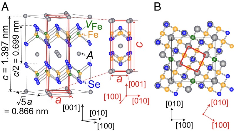
Recently, superconductivity was discovered at 32 K in a layered iron selenide, K0.8Fe2Se2 (7), which has drawn considerable attention, because this is the first material with a parent phase to exhibit an AFM insulating state among the iron-based superconductors (8). The A1–xFe2–ySe2 (A = K, Cs, Rb, Tl) system has the same crystal structure as the 122-type iron-based superconductor BaFe2As2 with a tetragonal ThCr2Si2-type structure (9) (Fig. 1A), and is composed of alternately stacked A and FeSe layers along the c axis. The Fe atoms in the FeSe layer form a square lattice, where the Se atoms are located at the apical sites of the edge-shared FeSe4 tetrahedra. However, the ideal chemical formula is A2Fe4Se5 (245 phase), which satisfies charge neutrality conditions with consideration of formal ion charges (i.e., +1 for A, +2 for Fe, and −2 for Se); therefore, the A and Fe sites include vacancies in the ThCr2Si2-type structure. It was shown that the Fe vacancies (VFe) in the parent 245 phase exhibit an order–disorder transition at ∼500 K and form a √5 × √5 × 1 supercell (the unit cell formula is A8Fe16Se20 with four VFe) (10), as shown in Fig. 1. Theoretical calculations suggested that the parent 245 phase is a Mott insulator with a Mott gap of ∼100 meV (11, 12). The gap was confirmed experimentally to be ∼430 meV (13). The 245 Mott insulator exhibits an AFM long-range order with TN as high as 470−560 K, similar to that of the cuprates, along with an ordered magnetic moment of more than 3 Bohr magneton (μB) at 10 K (10). Because of this similarity to cuprates (i.e., a Mott insulator with high TN), it is expected that a much higher Tc would be realized in a VFe-ordered AFM insulator of the 245 phase if the AFM order is suppressed by carrier doping.
Fig. 1.
Crystal structures of 122-type A1–xFe2–ySe2 (A = K, Cs, Rb, Tl) and 245-type parent-phase A2Fe4Se5 viewed along the [120] (A) and the [001] (B) directions. The spheres represent A (gray), Fe (orange), Se (blue), and Fe vacancy sites (VFe, green). The 122-type tetragonal fundamental cell and the 245-type √5 × √5 × 1 supercell are indicated by the red and black lines, respectively.
Indeed, chemical electron-doping of the 245 phase has been performed by reducing the VFe (2 − y > 1.93), which induced superconductivity at ∼30 K (8). However, it has been reported that these A1–xFe2–ySe2 superconductors intrinsically include phase separation into the superconducting phase, which is believed to exist in a phase without the VFe order, and the AFM-insulating phase (VFe-ordered 245 phase) (13). Further, there is controversy as whether the superconducting phase is an intercalated phase like Rb0.3Fe2Se2 (14), a VFe-free phase like KFe2Se2 (13), or this disordered VFe phase (15). The coexistence of such multiphases indicates that a well-controlled carrier doping structure of the 245 phase has yet to be realized by chemical-composition doping or substitution, and the carrier doping effects are not yet clear. In contrast, carrier doping by an electrostatic method that uses a field-effect transistor structure is free from this structural alternation and would be suitable for study of phase transitions in VFe-ordered 245 Mott insulators that have never become a superconductor.
In this study, we focused on the epitaxial films of one iron selenide Mott insulator, TlFe1.6Se2, because TlFe2–ySe2 is much more stable in air than the other A1–xFe2–ySe2 (A = K, Rb, Cs) (16), and a fully VFe-ordered phase with high chemical homogeneity has been obtained in single crystals due to the lower vapor pressure of Tl than those of alkaline metals (17). In addition, the number of VFe in TlFe2–ySe2 cannot be controlled over a wide range (the maximum 2 − y value is limited to only 1.6) regardless of the starting nominal compositions, and thus superconductivity has not previously been observed in TlFe1.6Se2 (16), although a bulk superconductivity was observed in mixed (Tl,K)1−xFe2−ySe2 (18). These features demonstrate that the TlFe1.6Se2 AFM insulator is the most ideal target to examine electrostatic carrier doping. We therefore used an electric double-layer transistor (EDLT) structure because the ionic liquid gate works as a nanometer-thick capacitor with a large capacitance and provides an effective way to accumulate a very high carrier density [maximum sheet carrier density of ∼1015 cm–2 under small gate voltages (VG) of around ±3 V]. This high carrier modulation by the EDLT can alter electronic states over a very wide range and convert even a band insulator into a metal, and even further, into a superconductor (19); similarly, a Mott insulator can be converted into a metal (20). We therefore expected that the EDLT structure would also modulate the carrier density sufficiently to induce a phase transition such as superconductivity in the iron selenide Mott insulator without chemical doping or structural alternation. Here, we used a single phase (i.e., homogeneous in structure, chemical composition, and vacancy distribution) and VFe-ordered TlFe1.6Se2 insulating epitaxial film grown by pulsed laser deposition (PLD) with an atomically flat surface as the transport channel layer of the EDLT. Large field-effect current modulation was demonstrated in the EDLT, particularly at low temperatures. The electric field clearly decreased the activation energy (Ea) and also induced a phase transition.
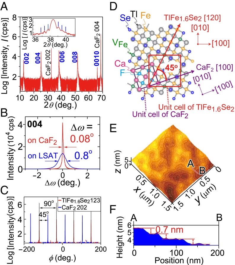
Fig. 2A shows the out-of-plane X-ray diffraction (XRD) pattern of a TlFe1.6Se2 thin film grown at the optimum temperature of 600 °C. Only the sharp peaks of the 00l diffractions of the TlFe1.6Se2 phase were observed, along with those of the CaF2 substrate, indicating that the film grows along the [00l] direction. Although the in-plane lattice parameter of CaF2 (a/√2 = 0.386 nm) is almost the same as that of (La,Sr)(Al,Ta)O3 (LSAT) (a/2 = 0.387 nm), the full width at half maximum (FWHM) values of the 004 rocking curve (Δω) of the film are much smaller when grown on the CaF2 substrate (0.08°) than that grown on the LSAT substrate (0.8°) (Fig. 2B). This suggests that an interface reaction occurs on the oxide LSAT substrate, whereas the fluoride CaF2 substrate is more suitable for TlFe1.6Se2; similar results are reported also for iron chalcogenide FeSe0.5Te0.5 epitaxial films (21). To confirm the epitaxial relationship between the TlFe1.6Se2 film and the CaF2 substrate, asymmetric diffractions were measured. Fig. 2C shows the results of ϕ scans of the 123 diffraction of the TlFe1.6Se2 film and the 202 diffraction of the CaF2 substrate. Both peaks appear every 90° and exhibit fourfold symmetry, substantiating the heteroepitaxial nature of the TlFe1.6Se2 film growth on the CaF2 substrate. Each peak (FWHM value = 0.2°) of the TlFe1.6Se2 film is rotated by 45° with respect to the peaks of the CaF2 substrate, showing that the TlFe1.6Se2 film grows on the CaF2 substrate with epitaxial relationships of [001] TlFe1.6Se2//[001] CaF2 (out of plane) and [310] TlFe1.6Se2//[100] CaF2 (in plane). These epitaxial relationships are a natural consequence of the smallest in-plane lattice mismatching [Δ(dTl–Tl − dCa–Ca)/dCa–Ca × 100 = 0.8%] as shown in Fig. 2D. Fig. 2E shows the surface morphology of the TlFe1.6Se2 epitaxial film on the CaF2 substrate. A flat surface with a step-and-terrace structure (root-mean-square roughness of 1.4 nm) was observed, indicating the layer-by-layer growth of TlFe1.6Se2 epitaxial films under optimized conditions. This result is also consistent with the observation of Pendellösung interference fringes (Fig. 2A, Inset). The step height (Fig. 2F) observed by atomic force microscopy is ∼0.7 nm, which agrees well with the distance between the nearest-neighbor FeSe–FeSe layers [corresponding to a half unit of the c-axis length (1.397 nm) of the TlFe1.6Se2 unit cell indicated in Fig. 1A]. These results guarantee that the TlFe1.6Se2 epitaxial film is of sufficiently high quality to be used for the EDLT transport channel.
Fig. 2.
(A) Out-of-plane XRD pattern of a TlFe1.6Se2 film grown on a CaF2 (001) substrate. (A, Inset) The magnified pattern around the 006 diffraction. The vertical lines indicate the positions of the Pendellösung interference fringes. (B) Rocking curves of the 004 diffractions of the TlFe1.6Se2 films on CaF2 and LSAT substrates. (C) ϕ scans of the 123 diffraction of the TlFe1.6Se2 film and the 202 diffraction of the CaF2 substrate. (D) In-plane atomic configuration of the TlFe1.6Se2 epitaxial film on the CaF2 substrate. (E) Topographic atomic force microscopy image of the surface of the TlFe1.6Se2 epitaxial film on the CaF2 substrate. (F) Height profile across the line A–B shown in E.
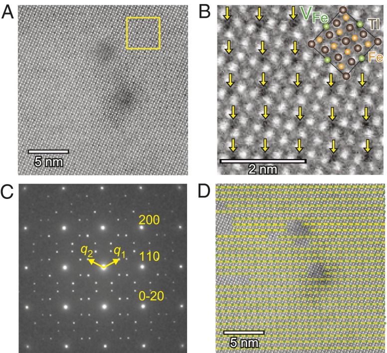
The atomic structure and VFe ordering in the TlFe1.6Se2 epitaxial film were examined by high-angle annular dark field scanning transmission electron microscopy (HAADF-STEM) and selected area electron diffraction (SAED). Fig. 3 A and B show the plan-view HAADF-STEM images of the TlFe1.6Se2 epitaxial film. VFe are detected as the dark regions due to the enhanced atomic number contrast of HAADF, showing the long-range periodic VFe ordering. In addition, superlattice diffractions due to the VFe ordering, similar to that of TlFe1.6Se2 single crystal (17), were observed in the SAED pattern Fig. 3C as indicated by q1 and q2. These results substantiate that the present sample is of a highly VFe-ordered phase. Fig. 3D demonstrates the arrangement of VFe more clearly by superimposing yellow lines on the HAADF-STEM image of Fig. 3A. Fully ordered VFe are dominant in almost the whole region, while small phase separation to disordered-VFe regions ≤5 nm in size (the unmarked regions in Fig. 3D) were also observed by keeping the perfect coherency of the fundamental crystal structure.
Fig. 3.
(A) [001] plan-view HAADF-STEM image of TlFe1.6Se2 epitaxial film. (B) Magnified HAADF-STEM image of the yellow square region in A. Vertical yellow arrows indicate the VFe sites with dark contrast. (B, Inset) The crystal structure of TlFe1.6Se2, where only Tl and Fe sites are shown because the positions of Se and Tl sites overlap over them (Fig. 1B). The square shows the superlattice unit cell, where VFe are shown (green circles). (C) The SAED pattern with electron beam along [001]. Two superlattice reciprocal vectors due to VFe ordering are indexed by q1 and q2. (D) Small green circles indicate all detected VFe, and yellow lines indicate VFe arrangement.
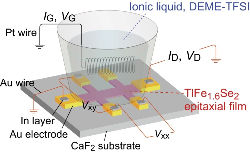
A 20 nm-thick TlFe1.6Se2 epitaxial film was used as the EDLT transport channel. Fig. 4 shows a schematic illustration of the EDLT, in which a six-terminal Hall bar channel and Au pad electrodes were formed using shadow masks. After pouring the ionic liquid, N,N-diethyl-N-methyl-N-(2-methoxyethyl)-ammonium bis-(trifluoromethylsulfonyl) imide (DEME-TFSI), into a silica glass cup, a Pt coil electrode was inserted into the ionic liquid to act as a gate electrode. The transfer curves [VG dependence of drain current (ID)] at a drain voltage (VD) of +0.3 V and output curves (ID vs. VD under various VG) of the EDLT were then measured.
Fig. 4.
Schematic of the EDLT using TlFe1.6Se2 epitaxial film with a six-terminal Hall bar structure on a CaF2 substrate. VG was applied via a Pt counter electrode through the ionic liquid, DEME-TFSI, contained in a silica glass cup. Electrical contacts were formed using Au wires and In/Au pads.
Fig. 5A shows the cyclic transfer characteristics (ID vs. VG) of the TlFe1.6Se2 EDLT at T = 280 K. A positive VG of up to +4 V was applied to the Pt coil gate electrode, which accumulates electrons at the interface. When VG = +1.7 V was applied, ID began to increase. The maximum ID in the transfer curve reached 12 μA at VG = +4 V, along with a small on:off ratio of 1.5. The gate leakage current (IG) (Fig. 5A, Lower) also increased at VG up to +4.0 V but was clearly smaller than ID in the whole VG region. After applying VG = +4 V, ID recovered to the initial values of 8 μA when VG was decreased to 0 V. The large hysteresis loop is observed due to the slow response of ion displacement in the ion liquid. Probably due to the same reason, some parallel shift remains in the second ID−VG loop; however, the shape and the hysteresis width are very similar to those of the first loop, guaranteeing the observed results are reversible and reproducible. These results demonstrate the electrostatic nature of carrier accumulation. In the output characteristics (Fig. 5B), the conductance dID/dVD increased with increasing VG at ≥ +2.0 V. Two output characteristics, which were measured before and after the transfer curve measurements in Fig. 5A, remain unchanged, which further guarantees the reversibility of the EDLT characteristics. However, the ID modulation is small at 280 K because of the high conductance at VG = 0, which originates from the highly naturally doped carriers in the TlFe1.6Se2 film, as reported for a TlFe1.6Se2 bulk crystal in which the carrier density was estimated to be ∼5 × 1021 cm–3 at T = 150 K (16). Using the reported gate capacitance value of ∼10 μF/cm2 (22), the maximum accumulated carrier density is estimated to be 2.5 × 1014 cm–2 at VG = 4 V, and the field-effect mobility in the linear region of the output characteristics is estimated to be 0.18 cm2/(V·s) at VG = +4 V. To estimate the carrier density induced in the TlFe1.6Se2 EDLT, we performed Hall effect measurements by applying magnetic fields of up to 9 T at temperatures between 300 and 25 K, but the Hall voltages (Vxy) obtained were below the detection limit of our measurement system. This suggests that the Hall mobility is smaller than 0.02 cm2/(V·s), which is roughly consistent with the small field-effect mobility above. Fig. 5C plots the VG dependence of the sheet conductance (Gs) at T = 300–25 K. The VG dependences of Gs were reversible also against repeated variation of measurement temperature (compare the open symbols and the filled symbols in Fig. 6A). With decreasing T, Gs at VG = 0 V steeply decreased from 2.2 × 10⁻⁵ to 1.5 × 10⁻⁸ S because of the decrease in carrier density. It should be noted that large Gs modulation with gains of three orders of magnitude was demonstrated at T = 25 K.
Fig. 5.
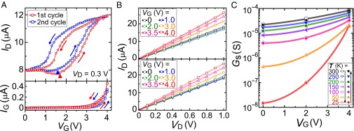
(A) Transfer characteristics (ID–VG) at VD = +0.3 V and T = 280 K cyclically measured for two loops. Arrows indicate the VG sweep directions, and triangles show the positions where ID begins to increase. IG vs. VG is also shown at the bottom. (B) Output characteristics (ID–VD) at VG = + 0−4 V and T = 280 K, measured before (Upper) and after (Lower) the transfer characteristics measurement in A. (C) VG dependence of Gs measured with decreasing T (open symbols) and increasing T (filled symbols) over the 25–300 K range. The solid lines are visual to show the change in Gs clearly.
Fig. 6.
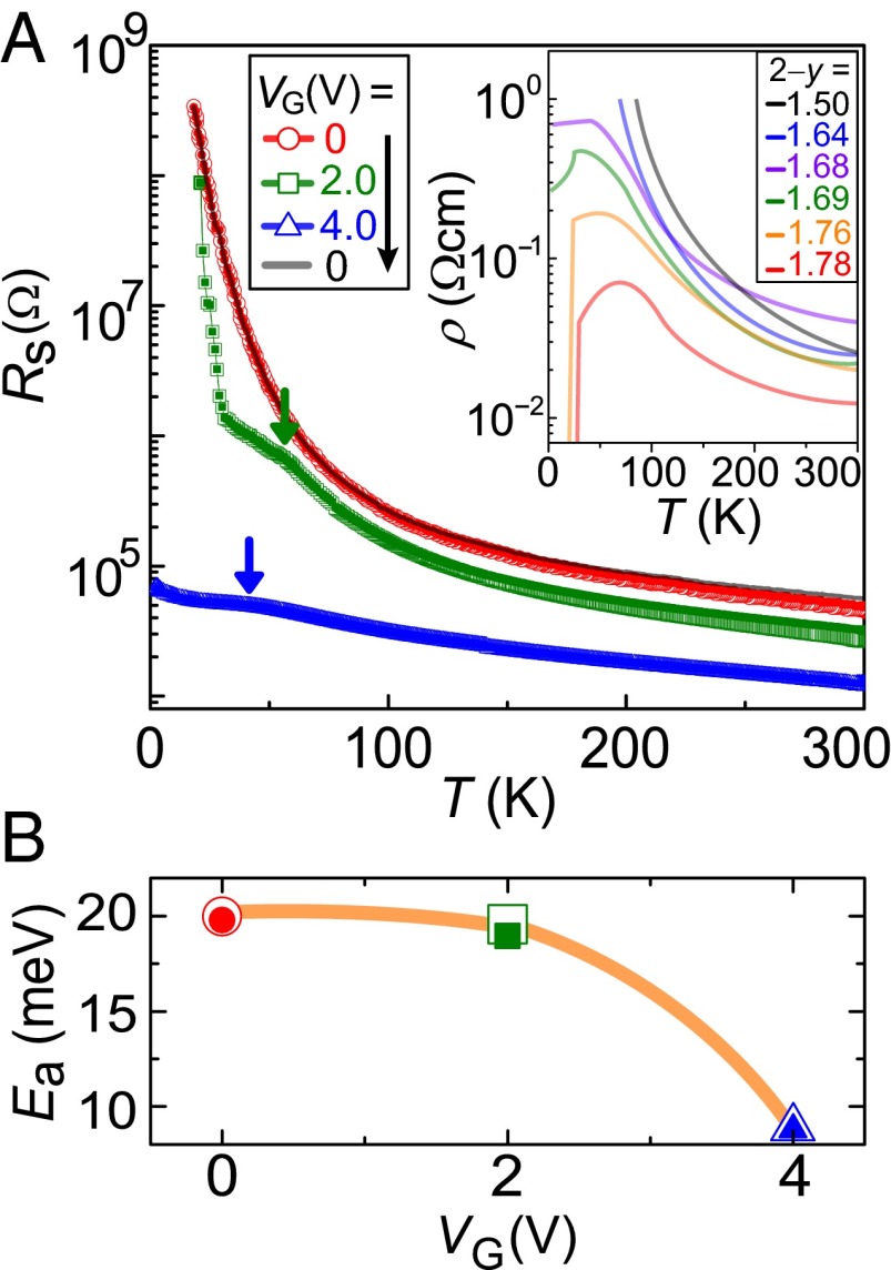
(A) T dependences of Rs for the TlFe1.6Se2 EDLT measured with increasing T (open symbols) and decreasing T (filled symbols) at VG = 0→+2.0→+4.0→0 V. The arrows indicate the positions of resistance humps. The reported ρ–T curves of (Tl,K) Fe2–ySe2 bulk materials (18) are shown for comparison (Inset). A resistance hump appears at 2 − y ≥ 1.68, and superconductivity emerges at 2 − y ≥ 1.76. (B) The Ea estimated from A in the high T region as a function of VG.
Fig. 6A shows the T dependences of the sheet resistance Rs (Rs–T) for the TlFe1.6Se2 EDLT at VG = 0, +2, and +4 V. The Rs–T characteristics from 300 to 30 K at VG = 0 V indicate simple thermally activated behavior, given by Rs = Rs0 exp(Ea/kBT) (where Rs0 is a constant and kB is the Boltzmann constant). This trend is similar to the Rs–T behavior of insulating TlFe2–ySe2 single crystals with 2 − y < 1.5 (18), but the resistivity anomaly due to a magnetic phase transition of spin reorientation at 100 K observed in the TlFe1.6Se2 single crystal (16, 17) was not detected. The Ea value of the TlFe1.6Se2 EDLT at VG = 0 obtained from the Arrhenius fitting is 20 meV (Fig. 6B). This value is smaller than the 57.7 meV of the TlFe1.47Se2 single crystal (18) but almost double that of TlFe1.6Se2 single-crystals (11 meV) (16). These observations indicate the naturally doped carrier density should be smaller than that of the TlFe1.6Se2 single crystals. On the other hand, Ea is far smaller than the calculated (∼100 meV) (11, 12) and experimentally measured Mott gaps (∼430 meV) (13), which suggests that the TlFe1.6Se2 film is doped with carriers.
The Rs–T behavior largely varied with VG, particularly in the low T region, which is seen also in Fig. 5C. The Rs–T curves were reversible in the cooling and heating cycles. The Ea value estimated in the high T region decreased from ∼20 meV at VG = 0−2 V to 8.9 meV at VG = +4 V (Fig. 6B); i.e., Rs at VG = +4 V is almost independent of T, indicating that a highly accumulated channel was formed by the application of VG. The Rs–T curves at VG ≥ 2 V do not show a simple thermally activated behavior and exhibit humps at T = 55 K for VG = +2 V and at 40 K for VG = +4 V (indicated by the vertical arrows in Fig. 6A). That is, when VG was increased from 0 to +2 V, the resistance hump appeared at Thump = 55 K, and Rs increased steeply again at T ≤ 31 K. At VG = +4 V, Thump shifted to a lower T (40 K), and Rs leveled off in the further lower T region. It would be possible to consider that the resistivity humps are attributed to a precursory phenomenon of a metal–insulator (MI) transition because Ea decreased sharply as confirmed in Fig. 6B. As for the A1–xFe2–ySe2 superconductor single crystals, they also exhibit resistance humps and cross-overs from an insulating state to a metallic state at Thump, and finally to a superconducting state (18). In the case of (Tl,K) Fe2–ySe2 in the literature (Fig. 6A, Inset) (18), the resistance hump appears at 2 − y = 1.68, and the superconductivity appears at 2 − y ≥ 1.76. This value is 16% larger than that of the TlFe1.6Se2 film in this work. This preceding work suggests that the Thump observed in this study can also be related to the MI transition and superconductivity; however, in this study we could not observe superconductivity up to the maximum VG of +4 V.
A similar phenomenon, which is attributed to a magnetic phase transition, has been observed also in fully VFe-ordered (100 K) (17) and multiphase (100–150 K) (23) TlFe1.6Se2 single crystals. On the other hand, the resistance humps are attributed to the formation of an orbital-selective Mott phase (OSMP) for the VFe-poor A1−xFe2–ySe2 bulk crystals, where one of the Fe 3d orbitals, dxy, remains localized and the other four orbitals are delocalized (24, 25). The Mott insulator phase dominates the resistance above Thump, whereas the OSMP prevails below it; finally, superconductivity appears below Thump of the OSMP transition at higher carrier doping levels. Due to these similarities, we consider that the resistance humps observed in this study are more likely assigned to the same origin of magnetic phase transition or OSMP.
In summary, electrostatic carrier doping of the Mott insulator iron selenide VFe-ordered TlFe1.6Se2 by the EDLT structure was demonstrated using a single-phase epitaxial film with an atomically flat surface grown on a CaF2 substrate. The EDLT structure, based on an ionic liquid gate, successfully controlled the conductance and induced the phase transition assignable to a magnetic phase transition or OSMP. This demonstration of carrier doping of the Mott insulator iron selenide by the electrostatic method offers a way to extend the exploration of high Tc superconductors even to insulating materials, in which chemical doping methods do not work.
Experiments
Film Growth and Characterization.
Epitaxial films of TlFe1.6Se2 were grown on fluorite-type CaF2 and mixed perovskite-type LSAT (001) single crystals by PLD. A KrF excimer laser (wavelength of 248 nm) was used to ablate a TlFe1.6Se2 polycrystalline target disk, which was synthesized using a two-step solid-state reaction. Fine pieces of the Tl metal and powders of FeSe and Se were mixed in a stoichiometric atomic ratio of Tl:FeSe:Se = 1:1.6:0.4 and sealed in an Ar-filled stainless steel tube. The mixture was first reacted at 400 °C for 5 h, and then at 650 °C for 10 h. The resulting powders were ground thoroughly and pressed into pellets, which were then placed in Ar-filled stainless steel tubes and heated at 650 °C for 16 h. All PLD target fabrication procedures except the heating process were carried out in an Ar-filled glove box. The base pressure of the PLD growth chamber used in this study was ∼10−5 Pa. The laser energy fluence and the repetition rate were 10 J/cm2 and 10 Hz, respectively. When grown in the 300–550 °C temperature range, epitaxial films were obtained, but their surfaces were relatively rough because of the 3D growth mode, whereas the FeSe impurity phase was detected at temperatures ≥650 °C. Thus, we concluded that the optimal growth temperature was 600 °C.
The film structures, including crystalline quality and the orientation of the crystallites, were examined by XRD (anode radiation: monochromatic CuKα1). The film thickness was characterized by X-ray reflectivity. The chemical composition of the film was checked by X-ray fluorescence measurements and electron probe microanalyzer (EPMA), and confirmed that the film’s chemical composition was the same as that of the PLD target. EPMA mapping indicated that composition of the epitaxial films was homogeneous with a spatial resolution of a few micrometers. The surface morphology of the film was measured with an atomic force microscope. The microstructure of VFe ordering in TlFe1.6Se2 epitaxial films was examined by HAADF-STEM and SAED. The STEM sample was prepared with a focused ion beam system. All these characterization measurements were performed at room temperature.
Device Fabrication and Characterization of Electrical Properties.
The 20 nm-thick TlFe1.6Se2 epitaxial films on the CaF2 (001) substrate were used as the transport channel of the EDLT. The TlFe1.6Se2 channel layer with a six-terminal Hall bar geometry (channel size: 500 μm long and 200 μm wide) and the Au pad electrodes were deposited using shadow masks. After bonding Au wires to the Au pads with In, a silica glass cup was placed on the devices and the Au wires were fixed with an epoxy adhesive. We used an ionic liquid, DEME-TFSI, as the medium for the gate electrode because it has a wide electrochemical potential window that extends up to +4 V and is free from water, which means that it is suitable for application to the EDLT. The ionic liquid was used to fill the silica glass cup and then a Pt coil was inserted into the ionic liquid to act as the gate electrode.
Transfer curves (i.e., the VG dependence of ID) and the output curves (ID vs. VD under various values of VG) were taken from the results gathered by a source measurement unit. The T dependence of Rs was measured by the four-probe method over a T range of 2–300 K. Because DEME-TFSI exhibits a glass transition from a rubber phase to a glass phase at T = 190 K, and the ion motion is frozen out at lower values of T, VG was applied at 300 K to form a highly accumulated gate structure, and then T was reduced while maintaining the same VG (26).
Acknowledgments
This work was supported by the Japan Society for the Promotion of Science (JSPS), Japan, through the “Funding Program for World-Leading Innovative R&D on Science and Technology (FIRST Program)” and by Ministry of Education, Culture, Sports, Science, and Technology (MEXT), Japan, through the “Element Strategy Initiative to Form Core Research Center.”
Footnotes
The authors declare no conflict of interest.
*This Direct Submission article had a prearranged editor.
References
- 1.Bednorz JG, Müller KA. Possible high Tc superconductivity in the Ba-La-Cu-O system. Z Phys B. 1986;64(2):189–193. [Google Scholar]
- 2.Kamihara Y, Watanabe T, Hirano M, Hosono H. Iron-based layered superconductor La[O1−xFx]FeAs (x = 0.05-0.12) with Tc = 26 K. J Am Chem Soc. 2008;130(11):3296–3297. doi: 10.1021/ja800073m. [DOI] [PubMed] [Google Scholar]
- 3.Schilling A, Cantoni M, Guo JD, Ott HR. Superconductivity above 130 K in the Hg-Ba-Ca-Cu-O system. Nature. 1993;363(6424):56–58. [Google Scholar]
- 4.Ren ZA, et al. Superconductivity at 55 K in iron-based F-doped layered quaternary compound Sm[O1–xFx]FeAs. Chin Phys Lett. 2008;25(6):2215–2216. [Google Scholar]
- 5.Tranquada JM, et al. Antiferromagnetism in YBa2Cu3O6+x. Phys Rev B. 1988;38(4):2477–2485. doi: 10.1103/physrevb.38.2477. [DOI] [PubMed] [Google Scholar]
- 6.Drew AJ, et al. Coexistence of static magnetism and superconductivity in SmFeAsO1−xFx as revealed by muon spin rotation. Nat Mater. 2009;8(4):310–314. doi: 10.1038/nmat2396. [DOI] [PubMed] [Google Scholar]
- 7.Guo J, et al. Superconductivity in the iron selenide KxFe2Se2 (0≤x≤1.0) Phys Rev B. 2010;82(18):180520. [Google Scholar]
- 8.Yan YJ, et al. Electronic and magnetic phase diagram in KxFe2−ySe2 superconductors. Sci Rep. 2012;2:212. doi: 10.1038/srep00212. [DOI] [PMC free article] [PubMed] [Google Scholar]
- 9.Rotter M, Tegel M, Johrendt D. Superconductivity at 38 K in the iron arsenide (Ba1-xKx)Fe2As2. Phys Rev Lett. 2008;101(10):107006. doi: 10.1103/PhysRevLett.101.107006. [DOI] [PubMed] [Google Scholar]
- 10.Ye F, et al. Common crystalline and magnetic structure of superconducting A2Fe4Se5 (A=K,Rb,Cs,Tl) single crystals measured using neutron diffraction. Phys Rev Lett. 2011;107(13):137003. doi: 10.1103/PhysRevLett.107.137003. [DOI] [PubMed] [Google Scholar]
- 11.Yu R, Zhu JX, Si Q. Mott transition in modulated lattices and parent insulator of (K,Tl)yFexSe2 superconductors. Phys Rev Lett. 2011;106(18):186401. doi: 10.1103/PhysRevLett.106.186401. [DOI] [PubMed] [Google Scholar]
- 12.Yan XW, Gao M, Lu ZY, Xiang T. Electronic structures and magnetic order of ordered-Fe-vacancy ternary iron selenides TlFe1.5Se2 and AFe1.5Se2 (A=K, Rb, or Cs) Phys Rev Lett. 2011;106(8):087005. doi: 10.1103/PhysRevLett.106.087005. [DOI] [PubMed] [Google Scholar]
- 13.Li W, et al. Phase separation and magnetic order in K-doped iron selenide superconductor. Nat Phys. 2012;8(2):126–130. [Google Scholar]
- 14.Texier Y, et al. NMR study in the iron-selenide Rb0.74Fe1.6Se2: Determination of the superconducting phase as iron vacancy-free Rb0.3Fe2Se2. Phys Rev Lett. 2012;108(23):237002. doi: 10.1103/PhysRevLett.108.237002. [DOI] [PubMed] [Google Scholar]
- 15.Chen F, et al. Electronic identification of the parental phases and mesoscopic phase separation of KxFe2−ySe2 superconductors. Phys Rev X. 2011;1(2):021020. [Google Scholar]
- 16.Sales BC, et al. Unusual phase transitions and magnetoelastic coupling in TlFe1.6Se2 single crystals. Phys Rev B. 2011;83(22):224510. [Google Scholar]
- 17.May AF, et al. Spin reorientation in TlFe1.6Se2 with complete vacancy ordering. Phys Rev Lett. 2012;109(7):077003. doi: 10.1103/PhysRevLett.109.077003. [DOI] [PubMed] [Google Scholar]
- 18.Fang MH, et al. Fe-based superconductivity with Tc=31 K bordering an antiferromagnetic insulator in (Tl,K) FexSe2. Europhys Lett. 2011;94(2):27009. [Google Scholar]
- 19.Ueno K, et al. Electric-field-induced superconductivity in an insulator. Nat Mater. 2008;7(11):855–858. doi: 10.1038/nmat2298. [DOI] [PubMed] [Google Scholar]
- 20.Nakano M, et al. Collective bulk carrier delocalization driven by electrostatic surface charge accumulation. Nature. 2012;487(7408):459–462. doi: 10.1038/nature11296. [DOI] [PubMed] [Google Scholar]
- 21.Tsukada I, et al. Epitaxial growth of FeSe0.5Te0.5 thin films on CaF2 substrates with high critical current density. Appl Phys Express. 2011;4(5):053101. [Google Scholar]
- 22.Ye JT, et al. Liquid-gated interface superconductivity on an atomically flat film. Nat Mater. 2010;9(2):125–128. doi: 10.1038/nmat2587. [DOI] [PubMed] [Google Scholar]
- 23.Cao H, et al. Evolution of the nuclear and magnetic structures of TlFe1.6Se2 with temperature. Phys Rev B. 2012;85(5):054515. [Google Scholar]
- 24.Yi M, et al. Observation of temperature-induced crossover to an orbital-selective Mott phase in AxFe2−ySe2 (A = K, Rb) superconductors. Phys Rev Lett. 2013;110(6):067003. doi: 10.1103/PhysRevLett.110.067003. [DOI] [PubMed] [Google Scholar]
- 25.Yu R, Si Q. Orbital-selective Mott phase in multiorbital models for alkaline iron selenides K1−xFe2−ySe2. Phys Rev Lett. 2013;110(14):146402. doi: 10.1103/PhysRevLett.110.146402. [DOI] [PubMed] [Google Scholar]
- 26.Yuan HT, et al. High-density carrier accumulation in ZnO field-effect transistors gated by electric double layers of ionic liquids. Adv Funct Mater. 2009;19(7):1046–1053. [Google Scholar]


