Abstract
A power-efficient wireless capacitor charging system for inductively powered applications has been presented. A bank of capacitors can be directly charged from an ac source by generating a current through a series charge injection capacitor and a capacitor charger circuit. The fixed charging current reduces energy loss in switches, while maximizing the charging efficiency. An adaptive capacitor tuner compensates for the resonant capacitance variations during charging to keep the amplitude of the ac input voltage at its peak. We have fabricated the capacitor charging system prototype in a 0.35-μm 4-metal 2-poly standard CMOS process in 2.1 mm2 of chip area. It can charge four pairs of capacitors sequentially. While receiving 2.7-V peak ac input through a 2-MHz inductive link, the capacitor charging system can charge each pair of 1 μF capacitors up to ±2 V in 420 μs, achieving a high measured charging efficiency of 82%.
Keywords: Adaptive capacitor tuning, capacitor charger, charging efficiency, inductive power transmission
I. Introduction
Inductive power transmission across the skin is currently the only viable solution to deliver sufficient power to implantable medical devices (IMDs) without imposing size and capacity constraints of rechargeable batteries [1]. In these IMDs, large capacitors have been utilized as temporary energy sources, which supply the low-power IMDs or augment the inductive power when it is interrupted or insufficient [2], [3]. Capacitors are also used in neural stimulation by storing charge and transferring it to the tissue periodically at high efficiency [4], [5]. Therefore, it is important to rapidly charge implanted capacitors efficiently not from batteries but directly through inductive transcutaneous links, while reducing the IMD size and the risk of tissue damage from overheating.
Charging capacitors from a voltage source through a switch achieves maximum 50% efficiency, wasting half of input energy in the switch. On the other hand, charging capacitors with a current source can minimize the switching loss as the fixed charging current becomes smaller [6]. Fig. 1 shows the conventional Li-ion battery charging techniques in inductively powered devices. AC–DC converters, e.g., a rectifier or a voltage doubler, convert an ac input voltage from an inductive link to a dc supply voltage VDD, resulting in ac–dc power loss [7]. In Fig. 1(a), the current source (CS) charges the capacitor directly without switches by controlling its gate voltage [8]. However, the current source still wastes energy because of the difference between supply and capacitor voltages VDD – VC. Generating an adaptive supply voltage AVDD in Fig. 1(b)−keeps the dropout voltage of the current source small AVDD – VC, while suffering from the additional dc–dc power loss [9]. The charging system in Fig. 1(c) utilizes a back telemetry link to control the inductive power, adjusting VDD depending on the VC level to reduce the voltage drop across the current source [10]. However, it requires additional sensing and control circuits as well as an external feedback loop through an optical link.
Fig. 1.
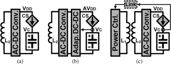
Conventional inductive Li-ion battery charging techniques in CS mode from (a) a fixed supply voltage [8], (b) an adaptive supply voltage [9], and (c) a supply voltage adjusted by an external control loop [10].
In this brief, we propose a novel capacitor charging system, which charges a bank of capacitors efficiently with a fixed charging current, directly from an ac input voltage through an inductive link. A series charge injection capacitor following the secondary L2C2 tank generates a predefined charging current, like a current source, while the voltage drop across this capacitor does not dissipate power. Consequently, the fixed charging current reduces the energy loss in the charger switches, boosting the capacitor charger efficiency. The proposed system can be utilized for a power-efficient neural stimulator which efficiently charges capacitor banks and injects charge into the neural tissue periodically [5]. In the rest of this brief, Section II describes the concept and implementation of the proposed wireless capacitor charging system. Section III presents circuit details and design considerations, including an active switch driver, an adaptive capacitive tuner, and a dual-output VTH-compensated rectifier. Measurement results are in Section IV, followed by conclusions in Section V.
II. System Architecture
A. Capacitor Charging Concept
The concept of the proposed capacitor charging system starts from utilizing a series charge injection capacitor as a current source, which generates a fixed amount of predefined charging current. Fig. 2 shows the simplified circuit diagram of the inductive capacitor charging system, which charges a pair of positive and negative capacitors CP and CN, respectively. The secondary coil L2 and its parallel resonant capacitor C2, which generate a coil voltage VCOIL, are followed by a series charge injection capacitor CS, which provides an input voltage VIN to CP and CN through switches SWP and SWN, respectively. SWP turns on when VIN > VCP form positive CP charging, and SWN turns on when VIN < VCN for negative CN charging with respect to the ground GND. When VCN < VIN < VCP, both switches turn off, and VIN follows VCOIL. Then, when either SWP or SWN turns on, the switch connects VIN to a positive or negative capacitor voltage VCP or VCN, holding VIN relatively constant and generating a fixed charging current ICH through CS. For example, when VIN > VCP, SWP connects VIN to VCP to hold VIN around VCP, while VCOIL keeps increasing. Thus, the voltage variation across CS, VCOIL – VIN, generates the positive ICH until VCOIL reaches its positive peak.When VCOIL starts decreasing from its peak, VIN also decreases below VCP, and SWP turns off. The charging current ICH can be expressed as
| (1) |
Fig. 2.
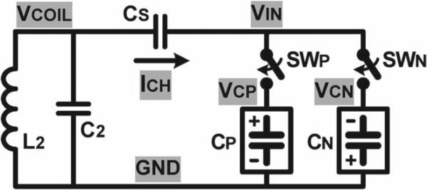
Simplified circuit diagram of the inductive capacitor charging system.
The ICH value can be adjusted by choosing proper CS, which will be discussed in Section II-B. Fixed ICH minimizes the switch loss, while unlike a real current source, the voltage drop across CS does not dissipate power, improving the charging efficiency from L2 to the capacitor pair.
B. Charging Time and Efficiency Analysis
The smaller the charging current, the higher the capacitor charging efficiency and the smaller the power loss in switches, leading to longer charging time. Hence, the charging current ICH should be optimized to charge the capacitors efficiently within a desired period. We modeled the charging time and efficiency depending on ICH with simplified voltage and current waveforms of the capacitor charging system in Fig. 3. In this analysis, fc is the carrier frequency that is received via VCOIL, n is the number of charging cycle, and t[n] is the transition time of VIN when VCN < VIN < VCP. In this simplified model, we assume the following: 1) VCOIL is sinusoidal with a constant peak voltage VPeak; 2) switches turn on and off at ideal times, and VIN becomes equal to VCP or VCN with negligible voltage drop across closed switches when connected to capacitors; 3) during each charging cycle, VCP and VCN are constant, and small voltage increments ΔVCP and ΔVCN are added to VCP and VCN at the end of each cycle, respectively; and 4) CP and CN are equal and charged by the same amount of ICH, i.e., VCP = –VCN.
Fig. 3.
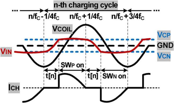
Simplified voltage and current waveforms of the capacitor charging system for modeling and theoretical analysis.
When VIN is connected to VCP or VCN for charging, VCOIL and ICH can be expressed as
| (2) |
| (3) |
VCP at the nth charging cycle VCP[n] can be obtained from
| (4) |
where ΔVCP[n] is the VCP increment at the nth charging cycle, from the initial condition of VCP[0] = VCN[0] = 0 V.
At the nth charging cycle, t[n] is equal to the transition time, in which VIN increases from VCN[n–1] to VCP[n–1]. Therefore,
| (5) |
In (5), t[n] can be written as
| (6) |
With t[n] in (6), ΔVCP[n] can be derived as
| (7) |
Therefore, the charging period TCH during which CP and CN are charged to a target charging voltage ±VTG at the nCHth charging cycle, can be obtained from
| (8) |
The total energy loss in SWP and SWN during nCH charging cycles ESW[nCH] can be calculated as a sum of switching energy losses in each cycle ΔESW[n]
| (9) |
| (10) |
where RSW is the switch resistance.
The capacitor charging efficiency ηCAP from L2 to the CP and CN pair of capacitors can be expressed as
| (11) |
where ECP and ECN are the stored energies in CP and CN, respectively, which are and , respectively, and ESYS is the energy consumed by the rest of the system during nCH charging cycles.
Smaller ICH increases TCH in (4)–(8), while smaller ICH and RSW increase ηCAP in (9)–(11). Therefore, when the maximum tolerable TCH is known, ICH can be selected to be as small as it takes TCH to charge CP and CN for CS and VPeak values in (3)–(8). CS should be smaller than CR, and VPeak > VTG.
C. Implementation of the Capacitor Charging System
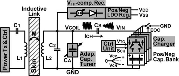
The overall architecture of the proposed capacitor charging system is shown in Fig. 4. A power transmitter drives the primary coil L1 at the designated carrier frequency fc, which induces VCOIL across L2. The capacitor charger consists of switches driven by high-speed active drivers to charge a bank of four pairs of capacitors CP and CN. A control unit sets a user-defined target charging voltage VTG and generates a sequence signal SCH to operate the four-channel capacitor charger sequentially, which can be utilized in a programmable multielectrode neural stimulation [5]. When charging, the capacitor charger connects VIN to positive and negative capacitors alternately to hold VIN at VCP or VCN, while generating the fixed charging current ICH through CS. In other words, CS operates like a current source that does not dissipate power, while reducing the switching loss in the capacitor charger and significantly improving the charging efficiency from L2 to the capacitor bank.
Fig. 4.
Overall architecture of the proposed power-efficient capacitor charging system through an inductive link.
In this capacitor charging system, the secondary resonance capacitance CR, connected across L2, can be expressed as
| (12) |
where C2 is the parallel resonant capacitor, CA is the adaptive tuning capacitor, and CEff is the effective capacitance of the capacitor bank, which varies as the capacitor bank voltage and switching duty cycle change. An adaptive capacitor tuner compensates for CEff variations by automatically adjusting CA to keep CR constant. Therefore, the secondary L2C2 tank is maintained at resonance during charging, while maximizing VCOIL. After the charging cycle, an end-of-charge (EOC) signal connects VIN to GND, and the adaptive capacitor tuner is deactivated, setting CR = C2 + CS. A dual-output VTH-compensated rectifier followed by low-dropout regulators generates the supply voltages VDD and VSS from VCOIL, which has little effect on the charging operation as long as the VCOIL amplitude is kept constant by the adaptive capacitor tuner.
III. Circuit Details and Design Considerations
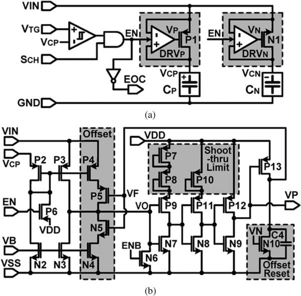
Fig. 5 shows the schematics of the capacitor charger and one of its active switch drivers. In Fig. 5(a), if VTG > VCP and SCH = high, the capacitor charger starts charging the capacitor bank CP and CN, with EN = high. When VIN > VCP, the active switch driver DRVP turns on the switch P1 with VP = low to provide the positive charging current +ICH to CP with a small switch loss. Fig. 5(b) shows the active switch driver (DRVP ) in which P2, P3, N2, and N3 form a common-gate comparator, whose inputs are connected to VCP and VIN. Since the current drawn from VIN is much smaller than the charging current, it has little effect on the charging operation. An offset block, which consists of current sources P4 and N4 and control switches P5 and N5, injects additional positive or negative offset current, depending on a feedback voltage VF, to expedite VO transition for fast P1 switching, maximize the forward current delivered to the capacitor, and minimize the back current to improve the charging efficiency [11]. Since the VO level depends on VIN amplitude, which varies during charging, shoot-through limited inverters level-shift VO to supply levels to drive P1 with proper VP levels. An offset reset switch N10, which is driven by VN, resets the offset by pulling VF = low after P1 turns off and VIN < VCN for the next CP charging cycle. Here, the timing of the reset signal depends on VIN, which, unlike the process-dependent inverter delay in [11], is independent of process variations. DRVN has a symmetrical structure with respect to DRVP.
Fig. 5.
Schematic diagrams of (a) the capacitor charger and (b) one of its active switch drivers DRVP.
Fig. 6 shows the schematic diagram of the adaptive capacitor tuner. A dynamic bias and envelope detector sense the positive VCOIL amplitude and compare it to a threshold window around VREF =1.2 V. If VCOIL is outside a designated window (2.7–2.8 VP), UP or DN signals from comparators CMP1 or CMP2 trigger a 7-bit up/down counter to progressively adjust a 7-bit binary-scaled set of tuning capacitors CA =0~127×(8 pF), between VCOIL and GND, to bring VCOIL amplitude back within this window. CA can accommodate the capacitance variations in (12), which result from CS (=1 nF in this system) in series with CEff as it varies with VCP,CN. The switches for tuning capacitors P17 to P23 are driven by VDDH, which is the higher voltage between VDD and VCOIL, to ensure proper turnoff.
Fig. 6.
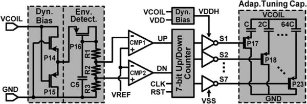
Schematic diagram of the adaptive capacitor tuner.
Fig. 7 shows the schematic diagram of the dual-output VTH-compensated rectifier. VCOIL is converted to two half waves VINP and VINN to prevent overvoltage across the following transistors that constitute a positive and negative rectifier pair, generating VRECP and VRECN, respectively. In the positive rectifier, VTH(P28) of the diode-connected transistor P28 compensates for VTH(P27) of the rectifying switch P27, resulting in a small voltage drop of VGS(P27) – VGS(P28) and high ac–dc power conversion efficiency. R4 reduces the gate voltage of P27 by discharging C6 in case VRECP decreases.
Fig. 7.
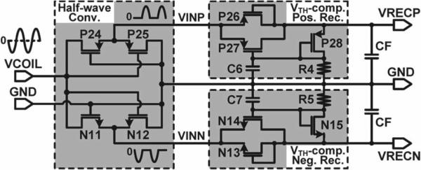
Schematic diagram of the dual-output VTH-compensated rectifier.
IV. Measurement Results
A. Chip Micrograph and Measured Waveforms
The four-channel capacitor charging system was fabricated in the TSMC 0.35-μm 4M2P n-well standard CMOS process, occupying 2.1 mm2. Fig. 8 shows the chip micrograph and floor plan of the charging system along with the inductive powering setup. A class-E power amplifier on the transmitter side drives the primary coil (L1 = 6.8 μH and ) at 2 MHz and delivers power across a 15-mm gap to the secondary coil (L2 = 1.2 μH and ).
Fig. 8.
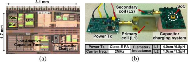
(a) Chip micrograph and (b) testing setup through an inductive link.
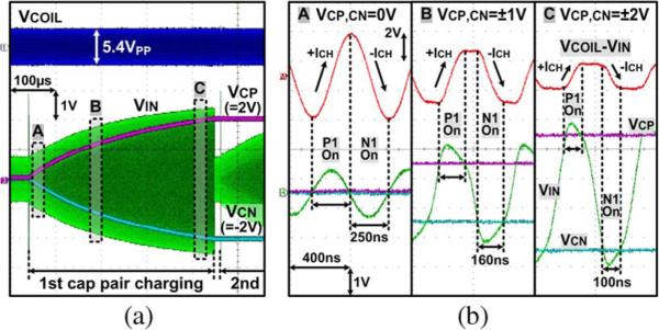
The waveforms in Fig. 9 show how the capacitor bank is being efficiently charged from VCOIL. In Fig. 9(a), the peaks of VIN follow VCP and VCN traces during charging because the fixed charging current ICH results in a small constant voltage drop across the capacitor charger switches P1 and N1. With CP = CN = 1 μF, each capacitor pair was charged to VCP = 2 V and VCN = –2 V in 420 μs when VCOIL = 2.7 VP. Fig. 9(b) shows the active switching waveforms when VCP,CN = 0, ±1, and ±2 V. When VIN > VCP, P1 turns on, holding VIN to VCP plus voltage drop across SWP, and the voltage across CS, VCOIL – VIN, starts to increase, flowing +ICH into CP. As VCP increases, the switching duty cycle decreases while the slope of VCOIL – VIN remains almost the same, generating a fixed charging current.
Fig. 9.
Measured waveforms of (a) the capacitor charger and (b) its zoomed-in switching as VCP,CN of 1-μF capacitor pairs reach ±2 V in 420 μs.
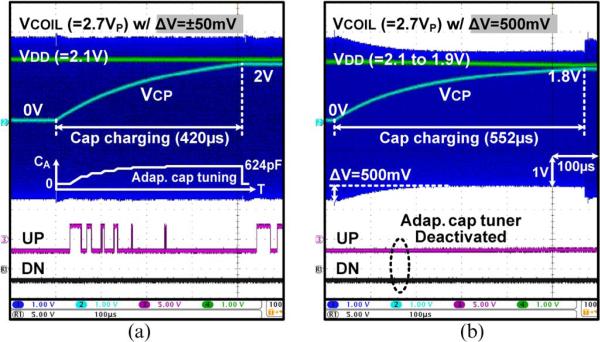
Fig. 10 shows how the adaptive capacitor tuner compensates for the CEff variations and maintains VCOIL amplitude constant during charging. In Fig. 10(a), the UP signal triggers the up/down counter, automatically increasing the adaptive tuning capacitor CA to 624 pF as VCP increases. Therefore, CA compensates for the CEff variations, and the secondary resonance capacitance CR in (12) stays at C2 + CS during charging, generating a relatively constant VCOIL with small ΔVCOIL = ±50 mV variations. In Fig. 10(b), where the adaptive capacitor tuner is deactivated, the VCOIL amplitude has dropped by 500 mV because of the resonance capacitor detuning, resulting in VDD reduction and limitation of VCP to only 1.8 V, instead of the 2-V target. Therefore, the adaptive capacitor tuner ensures proper charging operation with sufficient VCOIL amplitude against CR detuning.
Fig. 10.
Measured waveforms of VCOIL and VCP,CN variations during capacitor charging (a) with and (b) without the adaptive capacitor tuning mechanism.
B. Capacitor Charging Time and Efficiency
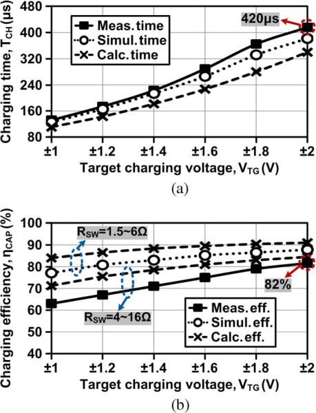
Fig. 11 shows the measured, simulated, and calculated values of the capacitor charging time and efficiency, while sweeping the target charging voltage VTG from ±1 to ±2 V, to verify the accuracy of our measurement as well as provide insight for further improvements. The calculated charging time and efficiency have been derived from (4)–(8) and (9)–(11) in Section II-B, respectively, with fc = 2 MHz, CS = 1 nF, CP = CN = 1 μF, and VPeak = 2.7 V. We assumed that RSW = 1.5–6 Ω depending on VCP,CN and the system supply power PSYS = 400 μW from simulations. In Fig. 11(a), the 1-μF capacitor pair was charged up to ±2 V in 420 μs. The amount of charging current at each charging cycle gradually decreases as capacitors are charged up because VIN needs longer transition time t[n] in (6) before charging. Therefore, as the capacitor voltages increase, capacitors require longer charging time for the same amount of voltage increment. Shorter charging time in calculations is the result of the ideal switching of SWP and SWN, regardless of VCP,CN levels, which also indicates the maximum possible capacitor charging efficiency.
Fig. 11.
Measured, simulated, and calculated (a) capacitor charging time and (b) charging efficiency versus target charging voltage at fc = 2 MHz, CS = 1 nF, CP = CN = 1 μF, and VPeak = 2.7 V.
In Fig. 11(b), the charging efficiency was defined as the stored dc energy in the capacitor bank over the total input ac energy of the capacitor charging system. The highest efficiency of 82% was measured when 1-μF capacitors were charged up to VTG = ±2 V. Lower |VCP,CN increases RSW of P1 and N1 switches, leading to larger switching loss and lower charging efficiency as VTG decreases. Discrepancies between measured and simulated efficiencies mainly result from larger RSW of the chip, which was estimated about 4–16 Ω by observing voltage drops across switches, compared–to the simulated RSW = 1.5–6 Ω. The calculated charging efficiency with RSW = 4–16 Ω shows closer results to the measured efficiency. While RSW can be further reduced by optimizing the switch sizes, the proposed capacitor charging system achieves a high measured charging efficiency of 63%–82% with CP = CN = 1 μF charged up to ±1 ~ ±2 V in 132–420 μs. Table I summarized the specifications of the current inductive capacitor charging system prototype. Table II compares the estimated capacitor charging efficiencies ηCAP when the conventional Li-ion battery charging methods in Fig. 1 are applied to charge capacitors from 0 to 4.2 V in current source mode.
TABLE I.
Capacitor Charging System Specifications
| Overall System | Capacitor Charger | ||
|---|---|---|---|
| Process | 0.35 μm CMOS | # of channel | 4 |
| L2/C2/CS | 1.2μH / 4nF / 1nF | Target voltage | ±1 ~ ±2 V |
| Carrier freq. | 2 MHz | Charging off. | 63 ~ 82% |
| Coil distance | 1.5 cm | Charging time | 132 ~ 420 μs |
| Vcoil peak | 2.7 V | CP/CN | 1 μF / 1 μF |
| Area | 2.1 mm2 | PSupply(Charging) | 240 μW |
| Rectifier / Regulator | Adaptive Capacitor Tuner | ||
| VRECP / VRECN | 2.25 V / -2.25 V | Tuning bit | 7-bit |
| VDD / VSS | 2.1 V / -2.1 V | Adaptive cap. | 0 ~ 1024 pF |
| Rec. PCE | 72% w/50 kΩ | PStatic | 20 μW* |
Simulation
TABLE II.
Benchmarking Capacitor Charging Efficiency
| Ref. | VC(V) | VDD(V) | ICS(mA) | ηACDC(%)* | ηDCDC(%) | ηCHG(%)** | ηCAP(%)*** |
|---|---|---|---|---|---|---|---|
| [8] | 0~4.2 | 4.3 | 3 | 80 | - | 48.8 | 39 |
| [9] | 0~4.2 | VC+0.2 | 800 | 80 | 90 | 91.3 | 65.7 |
| [10] | 0~4.2 | VC+0.3 | 698 | 80 | - | 87.5 | 70 |
| This work | 0~±2 | 2.7VPeakAC (Vcoil) | 34 (max) | Not needed | - | 82 | 82 |
Power efficiency of the active rectifier in [7]
Charger efficiency, ηCHG = avg (VC / VDD)
ηCAP = ηACDC × ηDCDC × ηCHG.
V. Conclusion
We have demonstrated a power-efficient wireless capacitor charging system for inductively powered applications. A fixed charging current generated by applying part of the coil voltage across a series charge injection capacitor charges a capacitor bank with small energy loss, improving the charging efficiency. During charging, an adaptive capacitor tuner maintains the inductive link at resonance, providing a constant coil voltage within a designated window. The charging time and efficiency of the system have also been analyzed to provide designers with better insight toward maximizing the charging efficiency for given charging time and capacitor bank values. This system is expected to improve the overall power efficiency in IMDs that utilize capacitor banks for energy storage and stimulation [5].
Acknowledgments
This work was supported in part by the National Institute of Health under Grant 5R21EB009437 and in part by the National Science Foundation under Award ECCS-824199. This brief was recommended by Associate Editor G. Wang.
REFERENCES
- 1.Chen K, Yang Z, Hoang L, Weiland J, Humayun M, Liu W. An integrated 256-channel epiretinal prosthesis. IEEE J. Solid-State Circuits. 2010 Sep;45(9):1946–1956. [Google Scholar]
- 2.Duncan M. Distributed functional electrical stimulation system. 2006 Oct;24 U.S. Patent 7 127 287. [Google Scholar]
- 3.Jow U, Kiani M, Huo X, Ghovanloo M. Towards a smart experimental arena for long-term electrophysiology experiments. IEEE Trans. Biomed. Circuits Syst. 2012 Oct;6(5):414–423. doi: 10.1109/TBCAS.2012.2211872. [DOI] [PMC free article] [PubMed] [Google Scholar]
- 4.Kelly S, Wyatt J. A power-efficient neural tissue stimulator with energy recovery. IEEE Trans. Biomed. Circuits Syst. 2011 Feb;5(1):20–29. doi: 10.1109/TBCAS.2010.2076384. [DOI] [PubMed] [Google Scholar]
- 5.Vidal J, Ghovanloo M. Towards a switched-capacitor based stimulator for efficient deep-brain stimulation. Proc. IEEE EMBC. 2010 Sep;:2927–2930. doi: 10.1109/IEMBS.2010.5626290. [DOI] [PMC free article] [PubMed] [Google Scholar]
- 6.Paul S, Schlaffer AM, Nossek JA. Optimal charging of capacitors. IEEE Trans. Circuits Syst. I, Fundam. Theory Appl. 2000 Jul;47(7):1009–1016. [Google Scholar]
- 7.Lee H, Ghovanloo M. An integrated power-efficient active rectifier with offset-controlled high speed comparators for inductively-powered applications. IEEE Trans. Circuits Syst. I, Reg. Papers. 2011 Aug;58(8):1749–1760. doi: 10.1109/TCSI.2010.2103172. [DOI] [PMC free article] [PubMed] [Google Scholar]
- 8.Valle BD, Wentz CT, Sarpeshkar R. An area and power-efficient analog Li-ion battery charger circuit. IEEE Trans. Biomed. Circuits Syst. 2011 Apr;5(2):131–137. doi: 10.1109/TBCAS.2011.2106125. [DOI] [PubMed] [Google Scholar]
- 9.Chen M, Rincon-Mora GA. Accurate, compact, and power-efficient Li-ion battery charger circuit. IEEE Trans. Circuits Syst. II, Exp. Brief. 2006 Nov;53(11):1180–1184. [Google Scholar]
- 10.Chen JJ, Yang FC, Lai CC, Hwang YS, Lee RG. A high-efficiency multimode Li-Ion battery charger with variable current source and controlling previous-stage supply voltage. IEEE Trans. Ind. Electron. 2009 Jul;56(7):2469–2478. [Google Scholar]
- 11.Lee H, Ghovanloo M. An adaptive reconfigurable active voltage doubler/rectifier for extended-range inductive power transmission. IEEE Trans. Circuits Syst. II, Exp. Brief. 2012 Aug;59(8):481–485. doi: 10.1109/ISSCC.2012.6177017. [DOI] [PMC free article] [PubMed] [Google Scholar]


