

Abstract
A power-efficient wireless stimulating system for a head-mounted deep brain stimulator (DBS) is presented. A new adaptive rectifier generates a variable DC supply voltage from a constant AC power carrier utilizing phase control feedback, while achieving high AC-DC power conversion efficiency (PCE) through active synchronous switching. A current-controlled stimulator adopts closed-loop supply control to automatically adjust the stimulation compliance voltage by detecting stimulation site potentials through a voltage readout channel, and improve the stimulation efficiency. The stimulator also utilizes closed-loop active charge balancing to maintain the residual charge at each site within a safe limit, while receiving the stimulation parameters wirelessly from the amplitude-shift-keyed power carrier. A 4-ch wireless stimulating system prototype was fabricated in a 0.5-μm 3M2P standard CMOS process, occupying 2.25 mm². With 5 V peak AC input at 2 MHz, the adaptive rectifier provides an adjustable DC output between 2.5 V and 4.6 V at 2.8 mA loading, resulting in measured PCE of 72 ~ 87%. The adaptive supply control increases the stimulation efficiency up to 30% higher than a fixed supply voltage to 58 ~ 68%. The prototype wireless stimulating system was verified in vitro.
Keywords: Active charge balancing, adaptive rectifier, closed-loop supply control, head-mounted deep brain stimulation, implantable medical devices, inductive power transfer
I. Introduction
Implantable medical devices (IMDs) with stimulating function have been proven as effective therapies to alleviate neurological diseases or substitute sensory modalities lost due to diseases or injuries [1]–[3]. These implantable stimulators are capable of injecting a designated amount of charge into the human body (often the neuronal tissue) by providing a precise amount of output current or output voltage for a predefined period. Deep brain stimulation (DBS) is one of the most effective examples of such therapies to treat Parkinson's disease, tremor, and dystonia [4], [5]. Today's DBS devices use large primary batteries implanted in the chest area, where there is more space available, and their subcutaneous interconnects pass across the neck to reach the electrodes implanted deep in the brain [6]. Batteries need to be replaced every 2 ~ 5 years through surgery, and there is always risk of mechanical failure in interconnects due to head motion. A head-mounted DBS can eliminate hardship imposed by chest-implanted primary batteries and long interconnects across the neck, replacing them with transcutaneous inductive power transmission from a behind the ear (BTE) rechargeable energy source, similar to cochlear implants and hearing aids [7]–[10].
Fig. 1 shows the conceptual configuration of a head-mounted inductively-powered DBS system. The external processing unit, which includes a rechargeable battery, provides transcutaneous power and data through a pair of loosely coupled coils. The induced AC input across the implanted coil supplies the rest of the DBS implant through an efficient power management unit. The DBS system generates stimulus pulses, which are delivered to the stimulation sites via individual leads that are significantly shorter than those from the chest area, and therefore, less invasive and more suitable for high-density DBS [11]. Like other wirelessly-powered IMDs, high power efficiency is paramount in reducing the risk of tissue damage from overheating [12].
Fig. 1.

Conceptual configuration of a head-mounted inductively-powered DBS system in which power and data are transferred through the inductive link.
Typically, three types of stimulation mechanism have been utilized depending on the application: voltage-controlled stimulation (VCS), current-controlled stimulation (CCS), and switched-capacitor stimulation (SCS) [13]. While VCS enables power-efficient stimulation, tissue and electrodes impedance needs to be known accurately to control the stimulation charge [13]. Balancing the stimulation charge is quite complicated in VCS because the electrode impedance varies over time and position. If the residual charge, which accumulates in the tissue following stimulation pulses, exceeds a safety limit, electrolysis of extracellular fluid can lead to pH variations, causing both tissue and electrode damage [5]. Conversely, CCS has been widely used because of its precise charge control and safe operation [14]. However, traditional CCS has low power efficiency due to the dropout voltage across the current source, which can result in significant power loss depending on the stimulation site voltage. SCS takes advantages of both high efficiency and safety by using capacitor banks to store and transfer charge to the tissue [13], [15]. However, it requires several off-chip capacitors that may increase the IMD size. In addition, high efficiency capacitor charging circuits from an AC input are needed to improve the overall DBS efficiency.
In order to achieve both safe and power efficient stimulation, we chose CCS with adaptive supply control, i.e., the stimulator supply voltage is automatically adjusted near the required stimulation voltage by detecting the site potential and forming a closed control loop through a power-efficient adaptive rectifier. This mechanism minimizes the voltage drop across the current sources, resulting in high power efficiency in the CCS. Our proposed wireless stimulating system also adopts active charge balancing by sharing the closed-loop path of the adaptive supply control to inject small current pulses in the tissue to keep the residual charges within a safety limit. Section II presents the proposed inductively-powered wireless stimulating system and compares it to prior solutions. Section III describes the circuit details of the proposed adaptive rectifier with phase control feedback, and Section IV depicts the implementation of the wireless DBS with adaptive supply control and active charge balancing through voltage readout channels. Measurement results from bench-top and in vitro experiments are depicted in Section V, followed by concluding remarks in Section VI.
II. Inductively-Powered Wireless Stimulating System
Fig. 2 compares various inductively-powered stimulating structures including the proposed stimulator with adaptive supply control. All structures were assumed to provide bipolar and biphasic stimulation through a similar pair of electrodes. We have assumed that the inductive link can maintain its peak efficiency against reflected impedance variations as stimulator loading changes. This is possible via a multi-coil inductive link or an adaptive resonant load transformation [16], [17]. Here we focus on power efficiency of the stimulating IMD, which can be defined as the ratio of the AC input power from the secondary coil to the stimulator output power delivered to the tissue.
Fig. 2.

Various inductively-powered stimulating structures with (a) the conventional rectifier and regulator [3], (b) the fixed output rectifier [18], (c) the dynamic dc-dc converter [19], (d) the external closed-loop supply control [20], [21], and (e) the internal closed-loop supply control with the proposed adaptive rectifier.
The conventional inductively-powered CCS in Fig. 2(a) utilizes a rectifier to convert the AC input to a DC VREC, followed by a low-dropout regulator (LDO) to generate a fixed supply voltage, VDD [3]. This simple structure wastes a large portion of the input power across the LDO, which is needed to accommodate VREC variations, and the current source, while the loss increases as VSTIM, the required voltage to maintain stimulation current constant, becomes smaller. Lee proposed the fixed output rectifier in Fig. 2(b) to generate a predefined constant VREC without an LDO [18]. Eliminating the LDO reduced the loss, but the CCS loss was still dominant during stimulation, especially when .
The stimulator in [19] utilized a dynamic supply, VIN, from a DC-DC converter as shown in Fig. 2(c). It achieved high efficiency from VCS as well as coarse current controllability. However, it still required constant DC input, VREC, from the rectifier, which loss should be added to that of the DC-DC converter (ηDCDC). In Fig. 2(d), the inductive power delivered to the stimulator was adjusted through an external closed loop, changing VREC to be near the peak voltage of VSTIM, and leading to small power loss in CCS current sources [20], [21]. However, the external control loop via load-shift-keying (LSK), which adjusts the inductive power transmission, is prone to interference and can even be interrupted in a loosely-coupled inductive link, while increasing the system complexity. The passive rectifier also induced large AC-DC loss, which decreased the overall power efficiency [22]. While individually they suffer from their limitations, the methods used in these inductively-powered stimulating structures may be used together to further improve the power efficiency.
In the proposed inductively-powered stimulator, the adaptive rectifier with active switching is capable of generating a multilevel DC voltage, VREC, directly from the AC input voltage across L2 through an internal closed-loop control mechanism, shown in Fig. 2(e). Adjusting VREC changes the power consumption in the IMD, leading to Tx output power variation. Therefore, VREC, which directly supplies the CCS without an LDO, is adaptively adjusted close to the peak of VSTIM, resulting in small loss while benefiting from the advantages of the CCS. Moreover, the adaptive rectifier achieves high AC-DC power conversion efficiency (PCE) by adopting the phase control feedback and active synchronous rectification to improve the overall power efficiency of the inductively-powered stimulator.
The overall architecture of the proposed inductively-powered head-mounted DBS system is shown in Fig. 3. The power management block receives AC input through the inductive link, and converts it to the adjustable VREC depending on the rectifier phase control bits, which are defined by the peak voltage at the stimulation sites that sets VREF through the 3-bit resistor DAC (RDAC). The LDO generates the digital supply voltage, VDIG, for the low voltage digital blocks. The overvoltage protection (OVP) circuit monitors the peak of VINP,N and connects a de-tuning capacitor across the AC input to suppress AC voltages larger than a certain limit.
Fig. 3.

Overall architecture of the proposed inductively-powered head-mounted DBS system equipped with the adaptive supply control and the active charge balancing for both power-efficient and safe current stimulation.
Two stimulus current drivers, CCS1 and CCS2, which are adaptively supplied from VREC, drive four stimulating sites in a complementary fashion with high compliance voltage, increasing the stimulation power efficiency. The voltage readout channel reports the relative voltage difference between active sites to the off-chip microcontroller (MCU), closing the feedback loop that adjusts VREC. The same loop also manages active charge balancing via on-chip controllers, which inject additional current pulses into the tissue to bring the voltage difference between sites within a certain limit to guarantee safe stimulation. Forward data from the external Tx coil is recovered via amplitude-shift-keying (ASK) demodulation, setting the stimulation parameters and active channels. The back telemetry link utilizes LSK modulation by closing the short-coil (SC) switches across L2.
III. Adaptive Rectifier With Phase Control Feedback
A. Rectifier Phase Control
In order for the adaptive rectifier to generate the desired multilevel VREC, the rectifier turn-on time needs to be adjusted to limit the forward current, while achieving high PCE. Fig. 4 shows the simplified voltage waveforms of the rectifier depending on the turn-on time. Conventional rectifiers aim to generate the maximum VREC from VIN(AC) at high PCE. Thus they turn on as long as VIN(AC) > VREC, as shown in Fig. 4(a) [22]. Consequently, VREC becomes dependent on the VIN(AC) amplitude, and it is not internally adjustable. In Fig. 4(b), VREC can be adjusted by controlling the turn-on time around the peak of VIN(AC). If the turn-on period is reduced, the lower forward current reduces VREC as well. However, the large voltage drop between VIN(AC) and VREC during the turn-on period results in large power loss across the rectifying transistors, resulting in low PCE. To adjust VREC while maintaining high PCE, we controlled the rectifier turn-on phase as shown in Fig. 4(c). In this method, the rectifier turns on when VIN(AC) > VREC, similar to the conventional rectifiers. However, its turn-off timing is controlled to limit the forward current. Therefore, VREC is adjustable depending on the rectifier turn-on phase, while the small dropout voltage between VIN(AC) and VREC during the on period provides high PCE.
Fig. 4.
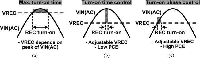
Simplified voltage waveforms of the rectifier with (a) the maximum turn-on time, (b) the turn-on time control, and (c) the turn-on phase control.
Fig. 5 shows the adaptive rectifier feedback model with the phase control mechanism. The threshold crossing detector sends a turn-on signal at phase θ to the synchronous rectifier when VIN(AC) > VREC(DC) to initiate the forward conduction. The phase control feedback compares VREC(DC)/3 with a reference voltage, VREF, which indicates the desired VREC level, and generates an error signal, e, that is amplified and converted to a time delay, TD. TD is then applied to the turn-on signal at phase θ to generate the delayed signal at phase θD using which the turn-off controller turns the rectifier off after TD. In other words, the rectifier conducts for TD from the onset of VIN(AC) > VREC(DC) at the turn-on phase of θ to adjust VREC, as shown in Fig. 4(c).
Fig. 5.

Adaptive rectifier feedback model showing the phase control mechanism.
B. Implementation of the Adaptive Rectifier
Fig. 6 shows the schematic diagrams of the adaptive rectifier with active switches and one of its phase control comparators. In Fig. 6(a), a pair of comparators, CMP1 and CMP2, which are equipped with the phase control feedback, drives the rectifying switches, P1 and P2, respectively, for low dropout voltage and high PCE. The reference voltage, VREF, which is provided through a 3-bit RDAC, controls the transition times of the comparator output voltages, VO1 and VO2, in a way that the rectifier turn-off timing can be adjusted to change the turn-on phase and consequently the VREC level. P1 and P2 turn on alternatively depending on VINP,N polarity, while a cross-coupled NMOS pair, N1 and N2, closes the rectifier current path. PMOS body terminals, VB1 and VB2, are connected to the highest potential among VINP,N and VREC with the dynamic body biasing circuit [23].
Fig. 6.

Schematic diagrams of (a) the proposed adaptive rectifier with active switches, and (b) one of its phase control comparators, CMP1.
In the phase control comparator (CMP1), shown in Fig. 6(b), P4, P5, N6, N7, P8, and N8 form a common-gate comparator with input voltages, VREC and VINP, while the current source, P7, injects additional current when VO1 is high and P6 turns on, forcing V1 to increase earlier and expedite the turn-on P1 transition of [24]. The phase control feedback loop consists of inverter chains along with the current-starved inverter, INV6 and N10, which bias current is controlled through AMP1 by comparing VREC/3 and VREF, to generate the corresponding time delay. INV6 output is further delayed before affecting the turn-off control transistor, P3, which forces the rectifier to turn off adaptively even before VINP < VREC to generate the desired VREC. Therefore, unlike conventional rectifiers or the voltage doubler-rectifier in [24], which output levels are dependent on the VINP,N amplitude, the adaptive rectifier is capable of generating variable supply voltages regardless of the VINP,N amplitude, thanks to the phase control feedback.
Fig. 7 shows the timing diagram of the adaptive rectifier depending on the actual VREC level vs. the target VREC, which is 3 × VREF. For example, when VREC > 3VREF in Fig. 7(a), AMP1 increases V2, decreasing the delay of INV6. Once VO1 drops to turn on the rectifier, P3 also turns on by VFB1 after a small delay, TD, limiting the charging period of the load and decreasing VREC. On the other hand, when VREC < 3VREF in Fig. 7(b), the delay of INV6 increases as V2 decreases, and P3 turns on after a longer TD or even remains off, allowing more forward current to increase VREC. When VREC = 3VREF in Fig. 7(c), V2 results in a TD that can maintain VREC at the desired value. Since the turn-off timing is controlled in every rectifier cycle, the ripple on VREC can be reduced to that of conventional rectifiers once it is settled on the desired VREC value.
Fig. 7.

Timing diagram of the adaptive rectifier when (a) VREC > 3VREF, (b) VREC < 3VREF, and (c) VREC = 3VREF.
In Fig. 6(b), a startup circuit with R1 and N5 driven by VINN guarantees the rectifier operation before VREC is charged up without additional startup circuits used in [24], and without affecting the normal rectifier operation after startup. The reset control circuit on the lower right resets the phase control feedback loop to turn off P3 and P6 after P1 turns off and VINP goes low. Here, the timing of the reset signal depends on VINP, which unlike the process-dependent inverter delay in [24], is independent of process variations.
IV. Wireless Stimulator With Adaptive Supply Control and Active Charge Balancing
A. Current Stimulator With Adaptive Supply Control
Each current driver has been equipped with a pair of 5-bit current sources with low dropout voltages,while being supplied from the adaptive VREC, as shown in Fig. 8. Feedback loops using AMP2–5 set the drain-source voltages of P14 ~ P18 and N15 ~ N19 at ~ 60 mV in the triode region. Therefore, the voltage head-room of the output stage, VHead, can drop down to VDS,sat + 60 mV, which is smaller than 2VDS,sat of a typical cascode output stage. The two current drivers source and sink at the same time through a pair of 4:1 site selectors, providing a bipolar stimulation compliance voltage of VREC – 2VHead. The 5-bit current sources with binary-weighted transistors are placed at the output stage directly to reduce the stimulator power loss compared to using current mirrors after a 5-bit current DAC in [20].
Fig. 8.

Schematic diagram of the proposed current driver with low dropout 5-bit current sources and the active charge balancing.
Active charge balancing circuits push or pull additional small current pulses to the load after stimulation until the residual site voltage settles within a ±50 mV safety window [25]. To prevent the accumulation of unrecoverable charge in the tissue and utilize the residual voltage as a reliable indicator of charge imbalance, the electrode potential needs to be kept within a safe potential window during stimulation as well. This is known as the water window, where irreversible Faradaic reactions do not occur [5]. The active charge balancing scheme, utilized here, is capable of providing the small balancing current pulses and also estimating the required balancing period. Passive charge balancing schemes which short electrodes after stimulation, on the other hand, have difficulty in defining the current and period needed for charge balancing [27].
In order to verify how the adaptive supply voltage, VREC, in Fig. 8 increases the stimulation power efficiency compared to using the fixed supply voltage, VDD, we analyzed the efficiency for both cases in Fig. 9. In Fig. 9(a), the electrodes and tissue model is simplified to a series RS and CDL, which represent the solution spreading resistance and the double-layer capacitance, respectively, while two current drivers across the two sites apply bipolar stimulation [26], [27]. Fig. 9(b) shows the stimulation current, ISTIM, and voltage, VSTIM, during the biphasic-bipolar stimulation with current amplitude, IS, and pulse width, TS. The power transferred to the load during cathodic and anodic stimulations can be expressed as the RS power loss plus the power charging or discharging CDL by simply multiplying the instantaneous ISTIM and VSTIM,
| (1) |
| (2) |
Fig. 9.

Stimulation efficiency analysis using (a) a simplified electrodes and tissue model (RS and CDL), and (b) stimulation current and voltage waveforms.
Negatively charged CDL after cathodic phase decreases VSTIM, and results in smaller power delivered to the load during the anodic phase. The stimulation power efficiency with the fixed supply voltage, VDD, can be defined as the ratio between the power transferred to the load and the power drained from the supply rails,
| (3) |
where IStatic is the static current of the stimulator internal circuitry, which is ~ 14 μA in our design, and usually much smaller than the stimulation current.
In the proposed current stimulator, the adaptive supply voltage, VREC, can be automatically adjusted as,
| (4) |
where VSTIM,peak and VCDL,peak are the peak voltages across the electrode-tissue model and the CDL, respectively, and VRS is the voltage drop across RS. By replacing VDD in (3) with VREC in (4), the stimulation power efficiency with the adaptive supply control can be expressed as,
| (5) |
which is indeed higher than ηSTIM(Fixed) in (3).
ηSTIM(Adap) in (5) can be further simplified as,
| (6) |
If (~ 150 mV in our design), ηSTIM(Adap) simplifies to a function of the electrode-tissue model parameters, RS and CDL, and stimulus pulse width, TS. Large RS results in more power transferred to the load, while large CDL or small TS decrease the required VREC, leading to higher stimulation efficiency.
B. Voltage Readout Channel and Forward/Back Telemetry
Fig. 10 shows the schematic diagram of the voltage readout channel including a capacitive attenuator and a voltage detector. VSTIM1 and VSTIM2, from the active sites, which can be as high as 4.6 V depending on the VREC, are capacitively attenuated by C8/(C8 + C9) during stimulation and charge balancing periods when EN = 1. After the charge balancing period, the capacitive attenuators are deactivated by disconnecting them from VSTIM1,2 (EN = 0) and then discharging C8 and C9 (ENB = 1) to attenuate VSTIM1,2 accurately in the next stimulation period. The attenuated stimulation voltages, VS1 and VS2, are applied to the voltage detector, which consists of a fixed-gain differential amplifier followed by a buffer, supplied at VDIG = 1.8 V. As a result, the differential input signals are converted to a single-ended output voltage, VDET, with a gain of R3/2R2, which is then provided to the MCU to close the loop on adaptive supply control and application of the active charge balancing function.
Fig. 10.

Schematic diagram of the voltage readout channel including the capacitive attenuator and voltage detector, which are used for both adaptive supply control and active charge balancing.
The proposed wireless stimulating system is capable of communicating with forward and back data telemetry through the inductive link. Fig. 11 shows the schematic diagrams of the clock and data recovery circuits, which are used for setting the stimulation parameters and active channels through the MCU. The clock recovery in Fig. 11(a) adopts the latch comparator with cross-coupled P23 and P24 followed by inverters to generate the clock signal from the power carrier, VINP,N, with low power consumption. The data recovery consists of an envelope detector and an amplitude shift keying (ASK) demodulator, as shown in Fig. 11(b) and (c), respectively.
Fig. 11.

Schematic diagrams of (a) the clock recovery, (b) the envelope detector, and (c) the ASK demodulator for the forward data telemetry.
In Fig. 11(b), the diode-connected passive rectifiers, P25 and P26, extract the envelope voltage, VENV, from the amplitude shift keyed power carrier, VINP,N. VENV is applied to the demodulator in Fig. 11(c), which includes a level shifter, a preamplifier, and a hysteresis comparator, to recover the data signal. The level shifter provides bias voltage to the rest of the circuit through P27, while shifting VENV down through P27-P28 to the preamplifier input range. The preamplifier has unbalanced delays, via R5 and C11, at its inputs, VIN1 and VIN2, to detect and amplify the amplitude variations of VENV. Finally, the hysteresis comparator, which utilizes the size mismatch of its current mirror, converts the preamplifier outputs to the recovered serial data bit stream at VDIG level through several inverters. The serial data is then oversampled by the clock signal in the MCU and saved in its registers. The back telemetry link utilizes the SC switches across L2, N3 and N4 in Fig. 6(a), to provide LSK modulation [22].
V. Measurement Results
The inductively-powered wireless stimulating system was fabricated in the ON-Semiconductor 0.5-μm 3M2P n-well standard CMOS process. Fig. 12 shows a chip micrograph and floor plan of the proposed wireless adaptive stimulating system, occupying 2.25 mm2 including pads. In our test setup, a class-E power amplifier drives the inductive link, which specifications are shown in Table I, to provide the wireless stimulating system with a 2 MHz sinusoidal input. The off-chip MCU (MSP430) from Texas Instruments (Dallas, TX) was chosen for its versatility and ultra-low power consumption [28].
Fig. 12.

Chip micrograph of the wireless stimulating system.
TABLE I.
In Vitro Test Setup Specifications
| Power transmitter | Class-E PA |
| Carrier frequency (fc) | 2 MHz |
| Primary coil diameter / inductance (L1) | 4.0 cm / 6.8 μH |
| Secondary coil diameter / inductance (L2) | 1.0 cm/1.2 μH |
| Distance between L1 and L2 | 1.5 cm |
| Electrodes (4-channel) | Quartz-platinum/tungsten |
| Electrode length / diameter / tip | 15 mm / 80 μm / 1 mm |
| Electrode spacing (pitch) | 3 mm |
| Electrodes + saline impedance @ 2.5 kHz | 3.8 kΩ + 80 nF in series |
A. Adaptive Rectifier With Adjustable
Measured waveforms in Fig. 13 show how the adaptive rectifier controls its turn-on phase depending on the 3-bit phase control input, CTL, to adjust VREC when VINP,N peak is constant at 5 V, load current is set to 2 mA, and fC = 2 MHz. When CTL = 000 and VREF = 0.83 V, the adaptive rectifier turns on within 50 ns of the beginning of the carrier cycle (θ = 36°), once VINP,N > VREC, and turns off after only 20 ns because the amount of delivered power is sufficient to increase VREC to the desired level of 2.5 V. When CTL = 011 and VREF = 1.13 V, the onset of rectifier turn-on shifts to 66 ns from the beginning of the carrier cycle (θ = 47.5°) and the on period adaptively increases to 28 ns to generate a higher VREC = 3.4 V. When CTL = 111 and VREF = 1.53 V, the adaptive rectifier operates almost like a regular active synchronous rectifier with θ = 68.4° and the on-time of 65 ns until VINP,N goes below VREC, while delivering more power to achieve the highest possible VREC = 4.6 V. In addition, when VREC = 2.5 V with IOUT = 2 mA, the adaptive rectifier results in a small ΔVREC < 3 mV against VIN,peak variations within 3 V to 5 V. This rapid line regulation capability is an additional benefit of the phase control feedback mechanism.
Fig. 13.

Measured waveforms of the adaptive rectifier generating the multilevel VREC from 5 V peak constant VINP,N depending on the 3-bit CTL input. In each case, IOUT is set at 2 mA and fC = 2 MHz.
Fig. 14 shows the adaptive rectifier PCE vs. VREC with VINP,N peak and load current kept constant at 5 V and 2.8 mA (the highest ISTIM = 2.48 mA for this stimulator), respectively. The adaptive rectifier achieves competitive PCEs of 78 ~ 94% and 72 ~ 87% in simulation and measurement, respectively, while providing unique multilevel adaptive VREC output between 2.5 ~ 4.6 V, controlled by its 3-bit input. The PCE slightly decreases with lower VREC because the rectifier dropout voltage becomes a larger percentage of VREC, and the on-resistance of the rectifying switches increases at lower voltages. Nonetheless, the adaptive rectifier still achieves considerably higher PCE than using a conventional rectifier followed by an adjustable regulator to generate the desired DC voltage. The difference between simulated and measured PCEs may be the result of mismatches between rectifying switches and their phase control comparators, as well as the effects of parasitic inductance and capacitance of the measurement setup, as explained in [22].
Fig. 14.

Measured and simulated PCE vs. VREC of the adaptive rectifier. Peak of VINP = VINN = 5 V, fC = 2 MHz, and IOUT = 2.8 mA.
B. Wireless Stimulator With Adaptive Supply Control and Active Charge Balancing
Measured waveforms of the stimulator outputs, VSTIM1,2, and the voltage detector output, VDET, are shown in Fig. 15 when ±1.04 mA biphasic-bipolar stimulus currents at TS = 400 μs flow between VSTIM1,2 through a series RSCDL load, which was chosen to be 2 kΩ and 500 nF for the DBS application [19], [29]. For closed-loop adaptive supply control, the MCU samples VDET at the end of the cathodic phase to measure VSTIM,peak in Fig. 9. The adaptive rectifier receives the phase control signals and automatically adjusts VREC to be 0.2 ~ 0.5 V higher than VSTIM,peak, to keep a small voltage drop across the stimulating current source, ΔV, for high stimulation efficiency. The MCU samples VDET again at the end of stimulation (anodic phase) to check the residual voltage between electrodes. If the voltage falls outside a safe window, set to ±50 mV, the active charge balancing circuit injects either a small positive or a negative current pulse (adjustable ±20 μA for 20 μs), and repeats the sampling procedure via the MCU until the residual charge is neutralized.
Fig. 15.

Measured waveforms of the current stimulator with RS = 2 kΩ and CDL = 500 nF connected in series between two active sites, as shown in Fig. 8, demonstrating the adaptive VREC control and active charge balancing operations through the voltage readout channel.
Fig. 16 compares the stimulator supply voltage and PCE vs. ISTIM graphs between adaptive, VREC, and fixed, VDD, supplies when RS = 2 kΩ, CDL = 500 nF, and TS = 400 μs. In Fig. 16(a), the adaptive VREC was measured with 0.3 V increments between 2.5 V and 4.6 V vs. ISTIM. In these measurements, VREC – VSTIM,peak < 0.2 V, while the fixed VDD was measured at 4.6 V. Fig. 16(b) compares the stimulation power efficiencies vs. ISTIM between the fixed and adaptive mechanisms, using the measured supply voltages in Fig. 16(a) as well as (3) and (5), respectively, while including the stimulator IStatic = 14 μA.
Fig. 16.

(a) Adaptive VREC and fixed VDD vs. ISTIM, (b) stimulation power efficiencies vs. ISTIM, and (c) overall power efficiencies, i.e., rectifier + stimulator, vs. ISTIM. Solid line: adaptive supply control, dashed line: fixed supply, electrode-tissue model: RS = 2 kΩ and CDL = 500 nF in series, and TS = 400 μs.
As expected, with lower ISTIM, the large voltage difference between VDD and VSTIM increases the power loss in the stimulator output stage (P21 and N22 in Fig. 8), degrading the fixed voltage stimulation power efficiency. On the other hand, the adaptive VREC keeps the voltage difference across the stimulator output small to minimize the power loss regardless of the ISTIM variations. As a result, the stimulation power efficiency with the adaptive supply control (58 ~ 68%) is up to 30% higher than the fixed VDD (31 ~ 63%). In Fig. 16(c), the overall power efficiencies from secondary coil, L2, to the load were calculated by multiplying the measured PCE of the adaptive rectifier in Fig. 14 and the stimulation efficiency in Fig. 16(b). Since the adaptive rectifier achieves relatively high PCEs even with lower VREC levels, adaptive supply control still leads to higher overall power efficiencies (41 ~ 58%) compared with using a fixed supply (27 ~ 55%).
The MCU consumes ~ 19 μA in the standby mode and ~ 400 μA for running the ADC and generating control signals at VDIG = 1.8 V and CLK = 2 MHz. Power consumption for these functions can be significantly reduced by sampling the peak stimulation voltage periodically, e.g., once every 10 ~ 20 cycles, to occasionally adjust the CTL. Moreover, the MCU functions can be integrated on chip by a low-power 3-bit SAR-ADC for generating the 3-bit CTL signal and simple control logic, leading to much lower power consumption compared to the off-chip MCU in the current prototype.
INL and DNL of the 5-bit cathodic/anodic stimulus currents, ISTIM1 and ISTIM2, for bipolar stimulation were measured and presented in Fig. 17 along with the stimulation current mismatch, ΔISTIM = ISTIM1 – ISTIM2. Both ISTIM1 and ISTIM2 show similar tendencies between 0.08 mA and 2.48 mA with 5-bit resolution, achieving the maximum INL and DNL of 0.43 and 0.17 LSB, respectively. The maximum ΔISTIM between ISTIM1 and ISTIM2 was ~ 4 μA.
Fig. 17.

Measured INL and DNL of the 5-bit ISTIM1 for cathodic stimulation and ISTIM2 for anodic stimulation along with the stimulation current mismatch, ΔISTIM, between ISTIM1 and ISTIM2.
Fig. 18 shows the measured waveforms of the clock recovery and the ASK-demodulated data recovery blocks for the forward data telemetry. In Fig. 18(a), a 2 MHz clock signal, CLK, has been recovered from the 2 MHz carrier signal. In Fig. 18(b), the amplitude variations of the primary coil voltage at 5.8% (= 3.8 V/65.2 V) modulation index, induced across L2, have resulted in ~ 100 mV variations in VENV. The ASK demodulator has then recovered the serial data bit stream, DATA, at 50 kbps.
Fig. 18.

Measured waveforms of (a) the 2 MHz clock recovery, and (b) 50 kbps data recovery from the 2 MHz power carrier at 5.8% ASK modulation index.
C. In Vitro Experiments
The proposed wireless stimulating system was verified through in vitro experiments using quartz-platinum/tungsten electrodes (EF8025, Thomas Recording, Giessen, Germany) and saline solution, as shown in Fig. 19. To emulate the DBS stimulation, 4 electrodes were aligned in parallel with 3 mm pitch spacing and soaked in 0.9% NaCl solution, which represents the brain tissue conductivity [30], [31]. The measured average impedance between adjacent electrodes in the solution was ~ 3.8 kΩ and 80 nF in series at 2.5 kHz. Table I summarizes the specifications of the in vitro test setup.
Fig. 19.

Test setup for in vitro experiments using the wireless adaptive stimulator including an inductive link operating at 2 MHz and 4 platinum/tungsten electrodes soaked in saline solution to emulate the DBS application.
Fig. 20 shows the measured stimulation waveforms from the in vitro experiments, focusing on the stimulator's adaptive supply control, active charge balancing, and multi-channel stimulation capabilities. In Fig. 20(a), two different stimulation currents, ±240 μA and ±480 μA, were applied to the saline solution through electrodes, and the supply voltage, VREC, was automatically set to 2.8 V and 3.4 V, respectively, which maximize the stimulation efficiency. At the same time, the active charge balancing mechanism ensured that the residual charge was neutralized following each biphasic stimulation. Fig. 20(b) shows the multi-channel stimulation waveforms among 4 electrodes. The selected channels sourced and sinked ±560 μA and 400 μs stimulus pulses at 250 Hz, while the other channels were floating.
Fig. 20.

Measured stimulation waveforms from the in vitro experiments showing (a) adaptive supply control with different stimulation currents, active charge balancing, and (b) multi-channel stimulation capability.
D. Performance Summary and Comparison
Table II benchmarks the proposed adaptive rectifier that was presented in Section III against several recently published active rectifiers. While being capable of generating multilevel output voltages between 2.5 V and 4.6 V from a constant 5 V peak AC input, the adaptive rectifier maintains high measured PCE of 72 ~ 87%, depending on the VREC level, when delivering 2.8 mA to the load. The voltage conversion efficiency, VCE (=VREC/VIN,peak), reaches as high as 92% when VREC = 4.6 V.
TABLE II.
Adaptive Rectifier Benchmarking.
| Publication | [32] | [33] | [34] | [22] | This work | |
|---|---|---|---|---|---|---|
| Technology | 0.5μm | 0.18μm | 0.35μm | 0.5μm | 0.5μm CMOS | |
| AC-DC Structure | Active Rec. | Active Rec. | Active Rec. | Active Rec. | Adaptive Output Active Rectifier | |
| VIN, peak (V) | 5 | 1.25 | 2.4 | 3.8 | 5 | |
| VREC(V) | 4.36 | 0.96 | 2.08 | 3.12 | 2.5 ~ 4.6 (3-bit) | |
| VCE (%) | 87.2 | 76.8 | 86.7 | 82.1 | 50 ~ 92 | |
| RL (kΩ) | 1 | 2 | 0.1 | 0.5 | IL = 2.8 mA | |
| fC (MHz) | 1 | 10 | 1.5 | 13.56 | 2 | |
| Area (mm2) | 0.4 | 0.86 | 0.4 | 0.18 | 0.3 | |
| PCE (%) | Sim. | 90.4 | N/A | 87 | 87 | 78 ~ 94 |
| Meas. | 84.8 | 76 | N/A | 80.2 | 72 ~ 87 | |
Table III summarizes the overall specifications of the proposed wireless stimulating system. The current stimulator achieves 58 ~ 68% power efficiency regardless of the ISTIM and VSTIM variations thanks to the adaptive supply control mechanism. It should be noted that the stimulation efficiency may also vary depending on the electrode/tissue impedance and the stimulus pulse width, as shown in (6).
TABLE III.
Wireless Stimulating System Specifications.
| Overall System | Current Stimulator | ||
|---|---|---|---|
| Process | 0.5 μm CMOS | # output ch. | 4-ch (DBS) |
| ASIC area | 2.25 mm2 | Stim. rate | 15.6 ~ 500 Hz* |
| Power source | Inductive link | Pulse width | 16 ~ 512 μs* |
| Power Management | Current range | 0.08 ~ 2.48mA (5b) | |
| Adjustable Vrec | 2.5 ~ 4.6V (3b) | INL / DNL | 0.43 / 0.17 LSB |
| Measured PCE | 72 ~ 87% | Ch. max. ΔI | 4 μA |
| Vdig | 1.8 V | IStatic | 14 μ** |
| OVP threshold | VIN,peak > 5.8V | VHead | 150 mV |
| Back telemetry | short-coil LSK | Charge balan. | Active pulse inject. |
| Forward Telemetry | Stim. PCE | 58 ~ 68%*** | |
| Clock freq. | 2 MHz | Voltage Readout Channel | |
| ASK data rate | 50 kbps | In/out range | 0 ~ 4.6 V/0.2 ~ 1.6 V |
| Modul. index | 5.8% | IStatic | 12 μA** |
Adjustable in MCU
Simulation
Vary with load model and pulse width
In the case of stimulating through multiple electrodes with different peak voltages, the adaptive supply voltage needs to follow the highest site voltage to properly stimulate all sites, limiting the improvement achieved in stimulation efficiency. This is why we recommend this technique for applications, such as DBS, which involve a relatively small number of macro sites that have similar properties. In applications with a large number of sites, such as retinal implants, it is conceivable to divide the sites into smaller subsets and use multiple independent adaptive rectifiers and current drivers, one per subset, at the cost of larger chip area.
The proposed system dissipates a maximum power of ~ 15 mW, assuming constantly flowing stimulus current, resulting in temperature rise well below the safe 1 °C limit [35]. If the efficiency of the transcutaneous inductive link is 60% at 10 mm coil separation from [36], the necessary Tx power at 2 MHz can be estimated at ~ 25 mW. This is well below the FCC's 100 mW/cm2 limit for maximum permissible exposure (MPE) within 0.3 ~ 3 MHz [37].
VI. Conclusion
Current-controlled stimulators (CCS) have been widely used in implantable electrical stimulators because of their precise current control and safe operation. However, CCS suffers from low power efficiency, which mainly results from the large voltage drop across the output current sources, especially when the necessary stimulation voltage is much smaller than the supply voltage. In order to improve the CCS power efficiency, we have proposed an internal closed-loop system for adaptive control of the stimulator supply voltage slightly above the peak of the stimulation voltage.
This mechanism significantly reduces the power loss in the CCS current sources, helping the CCS achieve high stimulation efficiency regardless of the stimulation voltage levels, while taking advantage of its safety features, completed by adopting the active charge balancing mechanism to neutralize the residual charge. The adaptive supply voltage has been generated directly from the inductive link using the proposed adaptive rectifier, which has high measured AC-DC PCE for the multilevel DC output thanks to the phase control feedback. The wireless stimulating system also includes a voltage readout channel to close the on-chip control feedback loop as well as an ASK demodulation block for forward data telemetry.
Stimulation power efficiencies with fixed and adaptive supplies have been derived and compared. Bench-top and in vitro measurement results of a fabricated prototype verified that the proposed inductively-powered wireless stimulating system with adaptive supply control was fully functional and improved the overall power efficiency of wireless stimulators for applications such as DBS and cochlear implants.
Biographies
 Hyung-Min Lee (S’06) received the B.S. degree in electrical
engineering (summa cum laude) from Korea University, Seoul, Korea,
and the M.S. degree in electrical engineering from the Korea Advanced Institute of
Science and Technology (KAIST), Daejeon, Korea, in 2006 and 2008, respectively.
Since 2009, he has been with the GT-Bionics Lab in the Department of Electrical and
Computer Engineering, Georgia Institute of Technology, Atlanta, GA, USA, where he is
working toward the Ph.D. degree.
Hyung-Min Lee (S’06) received the B.S. degree in electrical
engineering (summa cum laude) from Korea University, Seoul, Korea,
and the M.S. degree in electrical engineering from the Korea Advanced Institute of
Science and Technology (KAIST), Daejeon, Korea, in 2006 and 2008, respectively.
Since 2009, he has been with the GT-Bionics Lab in the Department of Electrical and
Computer Engineering, Georgia Institute of Technology, Atlanta, GA, USA, where he is
working toward the Ph.D. degree.
His research interests include analog/mixed-signal integrated circuits and power management integrated circuits for biomedical implantable systems.
Mr. Lee received Silver Prizes in the 16th and 18th Human-Tech Thesis Prize contest from Samsung Electronics, Korea, in 2010 and 2012, respectively, and the Commendation Award in the 4th Outstanding Student Research Award from TSMC, Taiwan, in 2010.
 Hangue Park (S’11) was born in 1980. He received the B.S. and
M.S. degrees from Seoul National University, Seoul, Korea, in 2006 and 2008,
respectively.
Hangue Park (S’11) was born in 1980. He received the B.S. and
M.S. degrees from Seoul National University, Seoul, Korea, in 2006 and 2008,
respectively.
From 2001 to 2004, he was with Bluebird-soft, where he designed circuit and system for industrial personal digital assistants (PDA). From 2008 to 2010, he worked for Samsung Electronics and designed SAW-less transceivers and PLLs for cellphone applications. He joined GT-Bionics Lab at the Georgia Institute of Technology, Atlanta, GA, USA, in 2010, where he is currently pursuing the Ph.D. degree. His research interest is in system and IC design for biomedical applications, especially in tongue-drive systems.
Mr. Park was a co-recipient of the Best Demonstration Award of the 2012 IEEE Biomedical Circuits and Systems Conference.
 Maysam Ghovanloo (S’00–M’04–SM’10)
was born in Tehran, Iran, in 1973. He received the B.S. degree in electrical
engineering from the University of Tehran, Tehran, Iran, in 1994, the M.S. degree in
biomedical engineering from the Amirkabir University of Technology, Tehran, Iran, in
1997, and the M.S. and Ph.D. degrees in electrical engineering from the University
of Michigan, Ann Arbor, MI, USA, in 2003 and 2004, respectively.
Maysam Ghovanloo (S’00–M’04–SM’10)
was born in Tehran, Iran, in 1973. He received the B.S. degree in electrical
engineering from the University of Tehran, Tehran, Iran, in 1994, the M.S. degree in
biomedical engineering from the Amirkabir University of Technology, Tehran, Iran, in
1997, and the M.S. and Ph.D. degrees in electrical engineering from the University
of Michigan, Ann Arbor, MI, USA, in 2003 and 2004, respectively.
From 2004 to 2007, he was an Assistant Professor in the Department of Electrical and Computer Engineering, North Carolina State University, Raleigh, NC, USA. He joined the faculty of the Georgia Institute of Technology, Atlanta, GA, USA, in 2007, where he is currently an Associate Professor and the Founding Director of the Georgia Tech Bionics Lab in the School of Electrical and Computer Engineering. He has authored or coauthored more than 100 conference and journal publications.
Dr. Ghovanloo is an Associate Editor of the IEEE Transactions on Biomedical Circuits and Systems and the IEEE Transactions on Biomedical Engineering. He has received awards in the 40th and 41st Design Automation Conference (DAC)/International Solid-State Circuits Conference (ISSCC) Student Design Contests. He has organized special sessions and was a member of Technical Review Committees for several major conferences, including ISSCC and ISCAS, in the areas of biomedical circuits, sensors, and systems. He is a member of Tau Beta Pi, Sigma Xi, the IEEE Solid-State Circuits Society, the IEEE Circuits and Systems Society, and the IEEE Engineering in Medicine and Biology Society.
REFERENCES
- 1.Krames ES, Peckham PH, Rezai AR, editors. Neuromodulation. Oxford, U.K. Elsevier Ltd.; 2009. [Google Scholar]
- 2.Shahrokhi F, Abdelhalim K, Serletis D, Carlen P, Genov R. The 128-channel fully differential digital integrated neural recording and stimulation interface. IEEE Trans. Biomed. Circuits Syst. 2010 Jun;4(3):149–161. doi: 10.1109/TBCAS.2010.2041350. [DOI] [PubMed] [Google Scholar]
- 3.Chen K, Yang Z, Hoang L, Weiland J, Humayun M, Liu W. An integrated 256-channel epiretinal prosthesis. IEEE J. Solid-State Circuits. 2010 Sep;45(9):1946–1956. [Google Scholar]
- 4.Kuncel AM, Grill WM. Selection of stimulus parameters for deep brain stimulation. Clin. Neurophysiol. 2004 Nov;115(11):2431–2441. doi: 10.1016/j.clinph.2004.05.031. [DOI] [PubMed] [Google Scholar]
- 5.Merrill DR, Bikson M, Jefferys JGR. Electrical stimulation of excitable tissue: Design of efficacious and safe protocols. J. Neurosci. Methods. 2005 Feb;141:171–198. doi: 10.1016/j.jneumeth.2004.10.020. [DOI] [PubMed] [Google Scholar]
- 6.Moore SK. Psychiatry's shocking new tools. IEEE Spectrum. 2006 Mar;43(3):24–31. [Google Scholar]
- 7.Catrysse M, Hermans B, Puers R. An inductive power system with integrated bidirectional data-transmission. Sens. Actuators A. 2004 Sep;115:221–229. [Google Scholar]
- 8.Ghovanloo M, Najafi K. A wireless implantable multichannel microstimulating system-on-a-chip with modular architecture. IEEE Trans. Neural Syst. Rehab. Eng. 2007 Sep;15(3):449–457. doi: 10.1109/TNSRE.2007.903970. [DOI] [PubMed] [Google Scholar]
- 9.Sauer C, Stanacevic M, Cauwenberghs G, Thakor N. Power harvesting and telemetry in CMOS for implanted devices. IEEE Trans. Circuits Syst. I, Reg. Papers. 2005 Dec;52(12):2605–2613. [Google Scholar]
- 10.Wilson BS, Dorman MF. Cochlear implants: A remarkable past and a brilliant future. Hearing Res. 2008 Aug;242(1–2):3–21. doi: 10.1016/j.heares.2008.06.005. [DOI] [PMC free article] [PubMed] [Google Scholar]
- 11.Martens HCF, Toader E, Decre MMJ, Anderson DJ, Vetter R, Kipke DR, Baker KB, Johnson MD, Vitek JL. Spatial steering of deep brain stimulation volumes using a novel lead design. Clin. Neurophysiol. 2011 Mar;122(3):558–566. doi: 10.1016/j.clinph.2010.07.026. [DOI] [PubMed] [Google Scholar]
- 12.Fujii T, Ibata Y. Effects of heating on electrical activities of guinea pig olfactory cortical slices. Eur. J. Physiol. 1982;392(3):257–260. doi: 10.1007/BF00584306. [DOI] [PubMed] [Google Scholar]
- 13.Vidal J, Ghovanloo M. Toward a switched-capacitor based stimulator for efficient deep-brain stimulation. Proc. IEEE Engineering in Medicine. and Biology Conf. (EMBC) 2010 Sep;:2927–2930. doi: 10.1109/IEMBS.2010.5626290. [DOI] [PMC free article] [PubMed] [Google Scholar]
- 14.Simpson J, Ghovanloo M. An experimental study of voltage, current, and charge controlled stimulation front-end circuitry. Proc. IEEE Int. Symp. Circuits and Systems (ISCAS) 2007 May;:325–328. [Google Scholar]
- 15.Kelly S, Wyatt J. A power-efficient neural tissue stimulator with energy recovery. IEEE Trans. Biomed. Circuits Syst. 2011 Feb;5(1):20–29. doi: 10.1109/TBCAS.2010.2076384. [DOI] [PubMed] [Google Scholar]
- 16.Kiani M, Jow U, Ghovanloo M. Design and optimization of a 3-coil inductive link for efficient wireless power transmission. IEEE Trans. Biomed. Circuits Syst. 2011 Dec;5(6):579–591. doi: 10.1109/TBCAS.2011.2158431. [DOI] [PMC free article] [PubMed] [Google Scholar]
- 17.Xue R, Cheng K, Je M. High-efficiency wireless power transfer for biomedical implants by optimal resonant load transformation. IEEE Trans. Circuits Syst. I, Reg. Papers. 2013 Apr;60(4):867–874. [Google Scholar]
- 18.Lee KFE. A timing controlled AC-DC converter for biomedical implants. IEEE Int. Solid-State Circuits Conf. (ISSCC) Dig. Tech. Papers. 2010 Feb;:128–129. [Google Scholar]
- 19.Arfin S, Sarpeshkar R. An energy-efficient, adiabatic electrode stimulator with inductive energy recycling and feedback current regulation. IEEE Trans. Biomed. Circuits Syst. 2012 Feb;6(1):1–14. doi: 10.1109/TBCAS.2011.2166072. [DOI] [PubMed] [Google Scholar]
- 20.Noorsal E, Sooksood K, Xu H, Hornig R, Becker J, Ortmanns M. A neural stimulator frontend with high-voltage compliance and programmable pulse shape for epiretinal implants. IEEE J. Solid-State Circuits. 2012 Jan;47(1):244–256. [Google Scholar]
- 21.Xu H, Noorsal E, Sooksood K, Becker J, Ortmanns M. A multichannel neurostimulator with transcutaneous closed-loop power control and self-adaptive supply. IEEE Eur. Solid-State Circuits Conf. (ESSCIRC) 2012 Sep;:309–312. [Google Scholar]
- 22.Lee H, Ghovanloo M. An integrated power-efficient active rectifier with offset-controlled high speed comparators for inductively-powered applications. IEEE Trans. Circuits Syst. I, Reg. Papers. 2011 Aug;58(8):1749–1760. doi: 10.1109/TCSI.2010.2103172. [DOI] [PMC free article] [PubMed] [Google Scholar]
- 23.Ghovanloo M, Najafi K. Fully integrated wide-band high-current rectifiers for wireless biomedical implants. IEEE J. Solid-State Circuits. 2004 Nov;39(11):1976–1984. [Google Scholar]
- 24.Lee H, Ghovanloo M. An adaptive reconfigurable active voltage doubler/rectifier for extended-range inductive power transmission. IEEE Trans. Circuits Syst. II. 2012 Aug;59(8):481–485. doi: 10.1109/ISSCC.2012.6177017. [DOI] [PMC free article] [PubMed] [Google Scholar]
- 25.Ortmanns M, Gehrke M, Tiedtke H. A 232-channell epiretinal stimulator ASIC. IEEE J. Solid-State Circuits. 2007 Dec;42(12):2946–2956. [Google Scholar]
- 26.Sooksood K, Stieglitz T, Ortmanns M. An active approach for charge balancing in functional electrical stimulation. IEEE Trans. Biomed. Circuits Syst. 2010 Jun;4(3):162–170. doi: 10.1109/TBCAS.2010.2040277. [DOI] [PubMed] [Google Scholar]
- 27.Sit J-J, Sarpeshkar R. A low-power blocking-capacitor-free charge-balanced electrode-stimulator chip with less than 6 nA dc error for 1-mA full-scale stimulation. IEEE Trans. Biomed. Circuits Syst. 2007 Sep;1(3):172–183. doi: 10.1109/TBCAS.2007.911631. [DOI] [PubMed] [Google Scholar]
- 28.MSP430F2132 Datasheet, Texas Instruments Inc. [Online] Available: http://www.ti.com/product/msp430f2132.
- 29.Wei XF, Grill WM. Impedance characteristics of deep brain stimulation electrodes in vitro and in vivo. J. Neural Eng. 2009 Aug;6(4) doi: 10.1088/1741-2560/6/4/046008. [DOI] [PMC free article] [PubMed] [Google Scholar]
- 30.Valente V, Demosthenous A, Bayford R. A tripolar current-steering stimulator ASIC for field shaping in deep brain stimulation. IEEE Trans. Biomed. Circuits Syst. 2012 Jun;6(3):197–207. doi: 10.1109/TBCAS.2011.2171036. [DOI] [PubMed] [Google Scholar]
- 31.DBS 3387, 3389 Lead Kit for Deep Brain Stimulation. Medtronic; Minneapolis, MN, USA: 2010. [Google Scholar]
- 32.Bawa G, Ghovanloo M. Active high power conversion efficiency rectifier with built-in dual-mode back telemetry in standard CMOS technology. IEEE Trans. Biomed. Circuits Syst. 2008 Sep;2(3):184–192. doi: 10.1109/TBCAS.2008.924444. [DOI] [PubMed] [Google Scholar]
- 33.Hashemi S, Sawan M, Savaria Y. A novel low-drop CMOS active rectifier for RF-powered devices: Experimental results. Microelectron. J. 2009 Jan;4011:1547–1554. [Google Scholar]
- 34.Guo S, Lee H. An efficiency-enhanced CMOS rectifier with unbalanced-biased comparators for transcutaneous-powered high-current implants. IEEE J. Solid-State Circuits. 2009 Jun;44(6):1796–1804. [Google Scholar]
- 35.Kim S, Tathireddy P, Normann RA, Solzbacher F. Thermal impact of an active 3-D microelectrode array implanted in the brain. IEEE Trans. Neural Syst. Rehab. Eng. 2007 Dec;15(4):493–501. doi: 10.1109/TNSRE.2007.908429. [DOI] [PubMed] [Google Scholar]
- 36.Jow U, Ghovanloo M. Design and optimization of printed spiral coils for efficient transcutaneous inductive power transmission. IEEE Trans. Biomed. Circuits Syst. 2007 Sep;1(3):193–202. doi: 10.1109/TBCAS.2007.913130. [DOI] [PubMed] [Google Scholar]
- 37.Questions and answers about biological effects and potential hazards of radiofrequency electromagnetic fields. Federal Communications Commission (FCC), OET Bulletin. 1999 Aug;56 [Google Scholar]