Abstract
In this work, we numerically demonstrate an all-optical tunable Fano resonance in a fishnet metamaterial(MM) based on a metal/phase-change material(PCM)/metal multilayer. We show that the displacement of the elliptical nanoholes from their centers can split the single Fano resonance (FR) into a double FR, exhibiting higher quality factors. The tri-layer fishnet MMs with broken symmetry accomplishes a wide tuning range in the mid-infrared(M-IR) regime by switching between the amorphous and crystalline states of the PCM (Ge2Sb2Te5). A photothermal model is used to study the temporal variation of the temperature of the Ge2Sb2Te5 film to show the potential for switching the phase of Ge2Sb2Te5 by optical heating. Generation of the tunable double FR in this asymmetric structure presents clear advantages as it possesses a fast tuning time of 0.36 ns, a low pump light intensity of 9.6 μW/μm2, and a large tunable wavelength range between 2124 nm and 3028 nm. The optically fast tuning of double FRs using phase change metamaterials(PCMMs) may have potential applications in active multiple-wavelength nanodevices in the M-IR region.
Recently, Fano resonance(FR) excited by an interference coupling between bright(radiating) modes and dark (non radiating) modes in metallic plasmonic nanostructures has been widely investigated1,2. It has generated much interest because of its application in the fields of chemical and biological sensing3,4, surface enhanced raman spectroscopy5, active plasmonic switching6, and slow light devices7. FR exhibits an asymmetric line shape with a sharp feature in transmission, reflection or absorption spectrum over an extremely narrow frequency range8,9. There have been a few attempts to create FRs in metallic plasmonic nanostructures, such as core-shell structure10, metallic nanowire arrays11,12, composite cut-wire structures13 plasmonic dimmers/clusters14 and photonic metamaterials(MMs)15,16,17,18. Among the various MMs, the configurations with broken symmetry are the most common approach for exciting narrow FRs. These asymmetric MMs give rise to a non-uniform electromagnetic environment around the resonators, leading to the effective coupling between bright modes and dark modes19.
The ability to control the central wavelength of a FR in MMs can find more flexible and critical applications in practice such as tunability of dispersion and group velocity of light18, multispectral imaging/detection20,broadband delay lines21.However, most researchers focus on passive tuning of FRs by adjusting geometric parameters of the MMs22,23,24,25,26 which limits the scope of applications. Recently, active tuning of the optical response of MMs has attracted growing interest owing to its ultra-short modulation time and on-to-off switching capabilities27,28. Therefore, for the purpose of actively controlling FRs, MMs integrated with optically active materials is a promising approach. Quite recently, a variety of approaches to modulate FRs in active MMs have emerged. Pryce et al exploited tunable FRs in MMs by means of mechanical deformation of an elastomeric substrate29. Belotelov et al presented a magnetically tunable FR in a magneto-plasmonic MM30. Kurter et al reported cryogenic temperature-dependent electromagnetically induced transparency(EIT) MM31 Samson et al demonstrated a frequency shift of a FR mode in a plasmonic planar MM by electrically tuning the dielectric properties of an adjacent chalcogenide glass layer32. Mousavi et al used the plasmonic response of graphene to tune a FR in the mid-infrared(M-IR) region33. However, FRs in these MMs are magnetically and electrically tuned hence only responding on a scale of several microseconds to seconds34. In addition, the integration of the required MM structures as well as the electrodes for the tuning of active dielectric layers can be difficult. Therefore, an appealing route that is notable for fast tunable FRs is to optically adjust the optical properties of the MMs. To this end, Gu et al presented active optical control of EIT MMs by integrating photoactive silicon(Si) islands into resonant elements18. However, this MM works only in the terahertz(THz) regime, and its structural geometry is complicated to fabricate in the optical region, which limits its potential use. Zhu et al proposed a fast all-optical tunable FR in the optical frequency range, using a plasmonic MM made of gold and polycrystalline lithium niobate (LiNbO3)8. However, this two dimensional (2D) planar MM system is based on a single metallic grating layer. It has been suggested that multiple layers of perforated metal–dielectric-metal(MDM) stacks with up to 100 to 200 layers along the propagation direction show a promising approach for three dimensional (3D) optical MMs35,36,37. Such 3D MMs can possess a thickness much larger than the free space wavelength in the optical region and excite a strong magneto-inductive coupling between neighboring functional layers under a normally incident light. The tight coupling between adjacent LC resonators through mutual inductance results in a low loss36. Thus 3D multilayer MMs are likely to be required for nearly all potential applications, such as cloaking and invisible materials35,36,37,38 as well as tunable metamaterials. Here we choose phase change material(PCM) as the dielectric interlayer,using which,we have previously shown designs for low loss tunable negative index material39 and a polarization independent tunable perfect absorber40.Thus, PCM based active tuning of FRs in three dimensional(3D) multilayer MMs is an interesting direction to pursue. To the best of our knowledge, it is still a formidable challenge to obtain a fast, low-power all optical tunable FR using 3D multilayer MMs in the optical regime.
Here, we numerically demonstrate that the resonant frequency of FRs can be optically tuned using PCMs in the mid-infrared(M-IR) region. Our structure is composed of an elliptical nanohole array (ENA) perforating through a Metal-Dielectric-Metal(MDM) trilayer, and a prototypical PCM: Ge2Sb2Te5, is selected as the dielectric layer. A single FR is observed in the symmetric MDM-ENA. This FR response is caused by the interaction between the bright and dark modes. The elliptical nanohole resonator array shows electric resonance (namely localized surface plasmon) which excite the bright modes, whereas MDM multilayers sustain a magnetic resonance (namely inductive-capacitive resonance) to induce the dark modes at the same frequency18,41. As soon as the elliptical holes are displaced from their central positions, the single magnetic resonance would be divided into two magnetic resonances at different wavelengths. A double FR appears, owing to the destructive interference between the electric resonance and the two magnetic resonances at different wavelengths. This interference can enhance the FR. By using Ge2Sb2Te5, a broad spectral tunability (from 2124 nm to 3082 nm) of the double FRs in the M-IR region can be obtained by switching between the amorphous and crystalline states of the PCMs42. Importantly, a heat model is constructed to examine the temporal variation of the temperature of the Ge2Sb2Te5 layer in the asymmetric MDM-ENA. The model shows that the temperature of the amorphous Ge2Sb2Te5 layer can be raised from room temperature to >433 K(phase transition point of Ge2Sb2Te5)43,44 in just 0.36 ns, with a low operating pump light intensity of 9.6 μW/μm2. Therefore, our proposed structure can rapidly tune the double FR under a low light intensity in the optical region using Ge2Sb2Te5. The optically active tuning of double FRs in these phase change metamaterials(PCMMs) may open up avenues for designing tunable multi-wavelength nanostructures in the optical regime such as slow light devices, ultrasensitive sensors and nonlinear devices. These PCMMs possess a simple geometry which remains compatible with standard photolithography patterning and can be easily experimentally realized in the optical region. Finally, it should be noted that PCMs do not require any energy to maintain the structural state of the material. Thus, once the MM has been switched it will retain its FRs until it is switched again. This obviously makes tunable FRs in PCMMs interesting from a ‘green technology' perspective.
Results
Metamaterials design
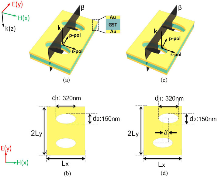
The proposed MM structures consist of two metallic films (30 nm thick Au) separated by a dielectric interlayer (160 nm thick Ge2Sb2Te5). Here, we simulate two sets of multilayer MMs starting from a symmetric element with both top and bottom elliptical holes exactly at the centre (see Fig. 1(a)–(b)) and then displaced the upper elliptical hole from the centre by a distance “δ” while keeping the lower elliptical hole fixed at the centre in order to break the symmetry (see Fig. 1(c)–(d)). For both structures, the elliptical nanohole array (ENA) (lattice constant, along the x axis is Lx = 500 nm, along the y axis is Ly = 400 nm; hole diameters, d1 = 320 nm, d2 = 150 nm) is perforated through the entire Au/Ge2Sb2Te5/Au structure, β is a cross-section plane of the structure, and the elliptical holes are periodically arranged in both the x and y directions. The Au bottom layer interacts with the upper Au layer to give rise to a closed circle of displacement current (JD) and localize an electromagnetic (EM) field within the dielectric interlayer. The structures are consider to be suspended in a vacuum, deep etching of a silicon support substrate can be used to achieve this. Au is selected as the metal due to its stability and low ohmic loss. The geometry of the unit cell pattern and the thickness of the sandwich layers have been chosen to allow for the impedance matching between the metamaterials and impinging plane wave45. The simulation is performed by commercial software Comsol, which is based on the Finite Element Method (FEM). The dielectric properties of Au as given by Johnson & Christy are used46. All the structures are excited by a source with a wavelength range from 1000 to 4000 nm, propagating along the negative z direction with the E field polarized along the small axis of the elliptical hole as shown in Fig. 1(a) and(c). The light source has a recurrence rate, fr = 25 kHz and pulse duration of 0.25 ns. The light fluence illuminating the sample from a single pulse is written as47
 |
where P0 = 3 mW is the total incident power, r is the distance from the beam center, w = 10 μm is Gaussian beam waist. To account for the periodic nature of the metamaterial, the model boundary at  and y = ±Ly is set to condition of perfect magnetic conductor and perfect electric conductor,respectively for normal incidence. Scattering boundary conditions are applied in the z direction. Adaptive meshes are generated by a built-in auto meshing algorithm of Comsol. The frequency dependent reflection r(ω) and transmission t(ω) are obtained from the S-parameters in the simulation package, and the absorbance is calculated as 1 − |r(ω)|2 − |t(ω)|2
48.
Figure 1.
(a) Schematic of the symmetric MDM-ENA(δ = 0 nm) consisting of a 160 nm thick Ge2Sb2Te5 dielectric layer between two 30 nm thick Au films perforated with a square array of elliptical holes suspended in a vacuum. (b) Illustration of the symmetric element of ENA, the lattice constants are Lx = 500 nm, Ly = 400 nm and hole diameters are d1 = 320 nm, d2 = 150 nm. (c) Schematic of the asymmetric MDM-ENA(δ = 70 nm) consisting of a 160 nm thick Ge2Sb2Te5 dielectric layer between two 30 nm thick Au films perforated with ENA suspended in a vacuum. (d) Illustration of the asymmetric element of ENA, the lattice constant is Lx = 500 nm, Ly = 400 nm, hole diameters are d1 = 320 nm, d2 = 150 nm, δ is the distance of the upper elliptical hole from the centre(δ = 70 nm).
Optical properties of Ge2Sb2Te5
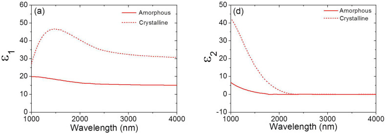
The real, ε1(ω) and imaginary, ε2(ω) parts of the dielectric function of Ge2Sb2Te5 in different phases are obtained from the experimental data in42, and for the mid-infrared (M-IR) spectral range the dielectric function is shown in Fig. 2; as can be seen there is a very large change in the dielectric function's real component. The dielectric constant of Ge2Sb2Te5 is very dispersive and has a non-negligible imaginary part. It also changes considerably during the reversible structural transformation from amorphous to crystalline. Different PCMs can display similar behavior in other parts of the spectrum. It should be mentioned that the reversible phase transition in Ge2Sb2Te5 is highly repeatable and more than a billion cycles have been experimentally demonstrated in data storage devices49.
Figure 2. Dielectric constant (a) ε1(ω) vs wavelength, (b) ε2(ω) vs wavelength for both amorphous and crystalline phases of Ge2Sb2Te5.
Tunability of double Fano resonance in the phase-change metamaterial
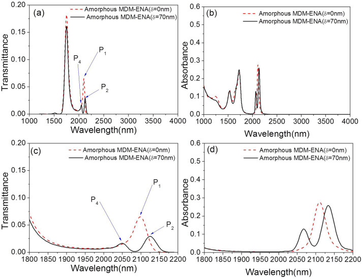
Figure 3 presents transmittance and absorbance for the structures of symmetric MDM-ENA(δ = 0 nm) and asymmetric MDM-ENA(δ = 70 nm) at normal incidence, where the dielectric layer is amorphous Ge2Sb2Te5.Here, we show that the symmetric MDM-ENA exhibits a single FR (denoted as P1 mode) with resonance wavelength centered at about 2098 nm (898.5 THz)(red dash curve in Fig. 3(a) with zoom-in in Fig. 3(c)). Spectral width of the single FR is 13.4 THz, leading to a quality factor(Q) of 67, where Q factor is defined by the resonant frequency over the width of the resonance50. It can be inferred that this single FR must be excited by the interaction between the electric resonance and the magnetic resonance in the structure. By displacing the upper elliptical hole from its centre by a distance δ = 70 nm, the single FR is split in two distinct resonant peaks at 2124 nm(887.5 THz) (marked as P2 mode) and 2050 nm (marked as P4 mode) by an asymmetric resonant dip. Namely, the single magnetic resonance at the wavelength of 2098 nm would be divided into two magnetic resonances at different resonance wavelengths of 2050 nm and 2124 nm by breaking the structural symmetry. Therefore, the double FR in the transmittance spectrum(black solid curve in Fig. 3(a)) is attributed to the destructive interference of the electric resonance(bright modes) with the magnetic resonances(dark modes) at different resonant wavelengths. In particular, a narrow transparency sub-band resonance window with a spectral width of 10.3 THz is achieved at P2 mode for the asymmetric MDM-ENA. It gives rise to a higher Q factor of 86 than the Q factor of 67 in the symmetric structure. This shows that asymmetric elements can significantly improve the FR in 3D multilayer MMs. In Figs. 3(b) and 3(d), one can observe that the absorbance in the asymmetric MDM-ENA is also split accordingly, whereas possessing a similar maximum value with the symmetric MDM-ENA.
Figure 3.
The comparison of (a) the transmittance, (b) the absorbance between asymmetric MDM-ENA(δ = 70 nm) with amorphous Ge2Sb2Te5 and symmetric MDM-ENA(δ = 0 nm) with amorphous Ge2Sb2Te5. (c) Zoom in picture of Fig. 3(a). (d) Zoom in picture of Fig. 3(b).
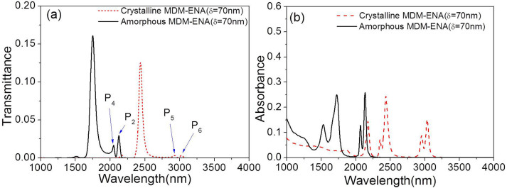
Figure 4 shows the evolution of the double FRs in both the transmittance and absorbance spectrums of the asymmetric MDM-ENA(δ = 70 nm) for M-IR radiation at normal incidence, in the amorphous and metastable cubic crystalline states. With the phase change of Ge2Sb2Te5, the double FR at 2124 nm (P2 mode) and 2050 nm(P4 mode) for the amorphous state shifts to a double FR at 2932 nm (P5 mode) and 3028 nm(P6 mode) for the crystalline state. Figure 4(b) presents the trapped plasmon mode absorbance lines of the structure for different states of Ge2Sb2Te5.The Ge2Sb2Te5 variable dielectric function gives rise to a concomitant tunability in the metamaterial absorbance. We also find that the peaks of both transmittance and absorbance drop down when Ge2Sb2Te5 changes from the amorphous to crystalline in addition to a shift, owing to a reduction in the impedance matching of the structure to vacuum.
Figure 4.
The comparison of (a) the transmittance, (b) the absorbance between the asymmetric MDM-ENA(δ = 70 nm) with amorphous Ge2Sb2Te5 and crystalline Ge2Sb2Te5.
Figure 5 shows total electric field intensity distributions  , total magnetic field intensity distributions
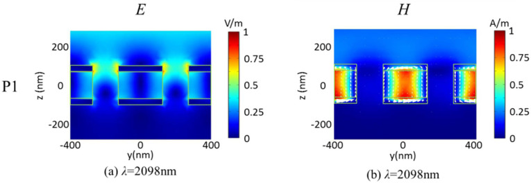
  and JD along the β plane at the resonant wavelengths of 2098 nm(P1 mode) for the symmetric MDM-ENA(δ = 0 nm) with amorphous Ge2Sb2Te5. Here, the arrows represent JD whereas the color represents the magnitude of the electromagnetic field intensities. In Fig. 5(b), the formation of the closed JD loops are observed to support a magnetic resonance at which light is trapped and strongly absorbed, thus the H field can be efficiently confined between two Au layers. However, Fig. 5(a) shows a low concentration of the E field intensity within the dielectric interlayer and elliptical apertures, indicating a weak electric resonance.
Figure 5.
3D-FEM simulation of (a) total electric field intensity distribution, (b) total magnetic field intensity distribution and JD distribution along β plane for the amorphous symmetric MDM-ENA(δ = 0 nm) at P1 mode(λ = 2098 nm).
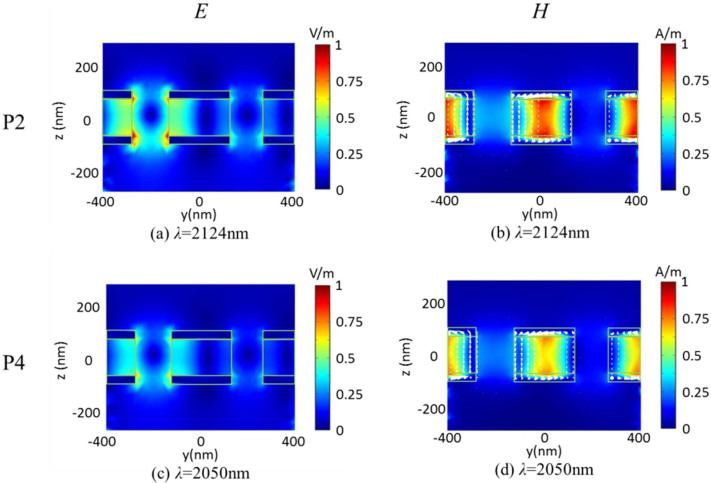
Figure 6 demonstrates E, H and JD along the β plane at the resonant wavelengths of 2124 nm (P2 mode) and 2050 nm(P4 mode) for the asymmetric MDM-ENA(δ = 70 nm) with amorphous Ge2Sb2Te5. Figure 6(b) shows that H field intensity distributions are still confined well within the dielectric layer at P2 mode. Whereas, Figure 6 (d) shows that H field intensity at P4 mode is weaker hence leading to a smaller magnetic resonance dipole than both P1 in Fig. 5(b) and P2 mode in Fig. 6 (b). Figure 6(a) and (c) show the E field intensity distributions at P2 and P4 mode, respectively. As can be seen, the E field intensity distributions at P2 mode in Fig. 6(a) are more efficiently concentrated thus giving rise to much stronger electric resonances than P1 in Fig. 5(a) and P4 mode in Fig. 6(c). Therefore, for the asymmetric MDM-ENA, the interaction of the stronger electric resonance and magnetic resonance leads to the narrower FR at P2 mode compared with P1 mode in the symmetric MDM-ENA.
Figure 6.
3D-FEM simulation of (a) total electric field intensity distribution, (b) total magnetic field intensity distribution and JD distribution along β plane, at P2 mode(λ = 2124 nm); (c) total electric field intensity distribution, (d) total magnetic field intensity distribution and JD distribution along β plane, at P4 mode(λ = 2050 nm) for the amorphous asymmetric MDM-ENA(δ = 70 nm).
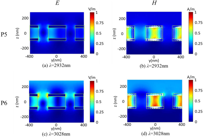
In Fig. 7(a)–(d),we present the distributions of E, H and JD associated with P5 (λ = 2932 nm) and P6 (λ = 3028 nm) modes for the asymmetric MDM-ENA(δ = 70 nm) with crystalline Ge2Sb2Te5. It demonstrates that the closed JD loops are still maintained at two resonance modes. It provides two magnetic dipolar moments thus leading to double resonant peaks. However, the double FRs is broadened owing to the inference between the weak magnetic resonances and electric resonances, resulting from the low intensities distributions of H and E fields in the structure.
Figure 7.
3D-FEM simulation of (a) total electric field intensity distribution, (b) total magnetic field intensity distribution and JD distribution along β plane, at P5 mode(λ = 2932 nm); (c) total electric field intensity distribution, (d) total magnetic field intensity distribution and JD distribution along β plane, at P6 mode(λ = 3028 nm) for the crystalline asymmetric MDM-ENA(δ = 70 nm).
Fano formula fitting to the transmittance spectrums simulated through FEM method
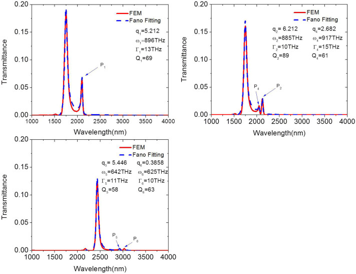
In Fig. 8, we fit the transmittance curves of both the symmetric MDM-ENA(δ = 0 nm) and asymmetric MDM-ENA(δ = 70 nm) using the FR lineshape in Eq.(2)51,52,53:
 |
where  , particularly, qi are the phenomenological shape parameters (so-called asymmetry parameters), ωi are the resonance frequencies and Γi, are the widths of the autoionized states (the resonance linewidth at half maximum, FWHM) of the resonant modes Pi53,54. With the parameters shown in Table 1, the calculated transmittances based on Eq.(1) approximately reproduce our FEM simulation data for the symmetric MDM-ENA(δ = 0 nm) with amorphous Ge2Sb2Te5, asymmetric MDM-ENA(δ = 70 nm) with amorphous and crystalline Ge2Sb2Te5, respectively.
Figure 8.
(a) 3D-FEM simulation of the transmittance spectrums (red solid) of the symmetric MDM-ENA with amorphous Ge2Sb2Te5 and best-fits to the FR lineshape Eq.(1) (blue dash); (b) 3D-FEM simulation of the transmittance spectrums (red solid) of the asymmetric MDM- ENA with amorphous Ge2Sb2Te5 and best-fits to the FR lineshape Eq.(1) (blue dash); (c) 3D-FEM simulation of the transmittance spectrums (red solid) of the asymmetric MDM- ENA with crystalline Ge2Sb2Te5 and best-fits to the FR lineshape Eq.(1) (blue dash).
Table 1. Parameters used in the FR lineshape to fit the transmittances of the MDM-ENA.
| Pi | qi | ωi(THz) | Γi(THz) | Qi |
|---|---|---|---|---|
| P1 | 5.212 | 896 | 13 | 69 |
| P2 | 6.212 | 885 | 10 | 89 |
| P4 | 2.682 | 917 | 15 | 61 |
| P5 | 5.446 | 642 | 11 | 58 |
| P6 | 0.3858 | 625 | 10 | 63 |
It is found that the Fano formula mostly matches the FEM simulation data around the resonant modes. Q factor is defined by the resonant frequency over the width of the autoionized state15,51, where the resonant frequency and the width of the autoionized state are obtained from the Fano formula fitting transmittance curves shown in Fig. 8.
Photothermal effect of the phase-change metamaterial
Since the reversible amorphous - crystalline phase transition of Ge2Sb2Te5 can be induced through optical heating, it is essential to understand the heat induced switching behavior of the asymmetric MDM-ENA. To show this, a heat transfer model is used to investigate the temporal variation of temperature of Ge2Sb2Te5 layer at normal incidence using the Finite Element Method(FEM) solver within COMSOL. The material thermal properties used for the simulation are summarized in Table 2. The thermal conductivity of Ge2Sb2Te5 changes with the temperature is obtained from the experiment data in55.
Table 2. Material thermal properties used in the Heat transfer model.
In this simulation, the thermal energy absorbed by one unit cell is defined as47
 |
where Lx = 500 nm is the lattice constant of the structure along the x axis; Ly = 400 nm is the lattice constant of the structure along the y axis; Ra = 0.0438 is the absorption coefficient of the structure, derived from the overlap integral between the light source power density spectrum and the absorbance spectrum, shown in Fig. 4(b). The heat source power is then described by a Gaussian pulse function
 |
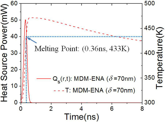
where τ = 0.15 ns is the time constant of the light pulse, t0 = 0.3 ns is the time delay of the pulse peak. Figure 9 shows Qs(r, t) and the temperature of the amorphous Ge2Sb2Te5 layer, where the structure is located at the center of Gaussian beam. The numerical simulation shows that the temperature within the amorphous Ge2Sb2Te5 dielectric layer is a function of the incident radiation flux and can exceed the amorphous to crystalline phase transition temperature of 433 K after 0.36 ns and a maximum of 472 K after 0.59 ns under a threshold incident flux of 9.6 μW/μm2. The temperature starts dropping after 0.59 ns before the next pulse arrives, due to heat dissipation to the surroundings.
Figure 9. 3D- FEM simulation of heat power irradiating on an amorphous asymmetric MDM-ENA located at the beam center, where the solid red line presents the heat power irradiating on the structures under normal incident intensity of 9.6 μW/μm2,the dash red line is the temperature of the amorphous Ge2Sb2Te5 layer during one pulse.
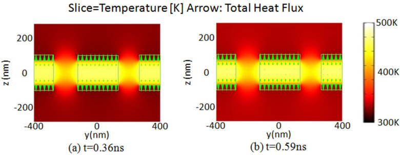
The temperature distributions of the structure at 0.36 ns and 0.59 ns along the plane β are shown in Fig. 10(a) and (b) respectively. One can observe that the temperature within the amorphous Ge2Sb2Te5 layer is uniform, and the dominant temperature gradient is towards the top and bottom Au films.
Figure 10. The temperature distribution of the unit cell of the amorphous asymmetric MDM-ENA along the β plane at (a) 0.36 ns and (b) 0.59 ns, where the color image indicates the temperature distribution and the arrows indicate the heat flux.
Discussion
In conclusion, we have numerically demonstrated a low-power and rapid all-optical tunable double FR in an asymmetric fishnet MMs based on a Au/Ge2Sb2Te5/Au multilayer. By breaking the symmetry in the ENA element, the single FR from the symmetric MDM-ENA splits into two resonant peaks, resulting in a double FR. This interference leads to a sharp transparency peak with higher Q factor. A wide wavelength shift of 42% for double FRs is observed in the M-IR region. This tunable effect is due to the phase transition from amorphous to crystalline. A heat transfer model is built to resolve the transient temperature variation in the structure during a photothermal process. Our model predicts that a fast phase transition time of 0.36 ns can be reached under a weak pump intensity of 9.6 μW/μm2.This work introduces a new approach for the study of ultralow-power and ultrafast photonic nanodevices. It may open up avenues for designing active multiple-wavelength slow light devices, plasmonics switching and sensors.
Methods
For the numerical calculations, we used the Finite Element Method by means of COMSOL Multiphysics. The unit cell of the phase-change metamaterial is shown in Fig. 1. The incident light is normal to the x-y plane with E field polarized in y direction. To account for the periodic nature of the metamaterial, the model boundary at  and y = ±Ly is set to condition of perfect magnetic conductor and perfect electric conductor, respectively for normal incidence.Scattering boundary conditions are applied in the z direction. The optical constant of gold is taken from the data of Johnson and Christy46.The dielectric function of Ge2Sb2Te5 in different phases are obtained from the experimental data in42.
Author Contributions
T.C., M.J.C. and R.E.S. conceived the idea of using phase-changed material for tuning the Fano resonance in the metamaterials. T.C. designed the metamaterial and performed numerical analysis. C.W.W. and L.Z. carried out the simulations and prepared the figures. T.C. supervised the research. T.C. and M.J.C. co-wrote the manuscript.
Acknowledgments
We acknowledge the financial support from National Natural Science Foundation of China (Grant No. 61172059 and 51302026), Ph.D Programs Foundation of Ministry of Education of China (Grant No. 20110041120015), Postdoctoral Gathering Project of Liaoning Province (Grant No. 2011921008), and The Fundamental Research for the Central University (Grant No. DUT12JB01).
References
- Papasimakis N., Fedotov V. A., Zheludev N. I. & Prosvirnin S. L. Metamaterial Analog of Electromagnetically Induced Transparency. Phys. Rev. Lett. 101, 253903 (2008). [DOI] [PubMed] [Google Scholar]
- Liu N. et al. Plasmonic analogue of electromagnetically induced transparency at the Drude damping limit. Nature Mater. 8, 758–762 (2009). [DOI] [PubMed] [Google Scholar]
- Liu S., Yang Z., Liu R. & Li X. High Sensitivity Localized Surface Plasmon Resonance Sensing Using a Double Split NanoRing Cavity. J. Phys. Chem. C 115, 24469–24477 (2011). [Google Scholar]
- O'Hara J. F. et al. Thin-film sensing with planar terahertz metamaterials: sensitivity and limitations. Opt. Express 16, 1786–1795 (2008). [DOI] [PubMed] [Google Scholar]
- Lombardi J. R. & Birke R. L. A Unified View of Surface-Enhanced Raman Scattering. Acc. Chem. Res. 42, 734–742 (2009). [DOI] [PubMed] [Google Scholar]
- Chang W. S. et al. A Plasmonic Fano Switch. Nano Lett. 12, 4977–4982 (2012). [DOI] [PubMed] [Google Scholar]
- Wu C., Khanikaev A. B. & Shvets G. Broadband Slow Light Metamaterial Based on a Double-Continuum Fano Resonance. Phys. Rev. Lett. 106, 107403 (2011). [DOI] [PubMed] [Google Scholar]
- Zhu Y., Hu X., Huang Y., Yang H. & Gong Q. Fast and Low-Power All-Optical Tunable Fano Resonance in Plasmonic Microstructures. Adv. Opt. Mater. 1, 61–67 (2013). [Google Scholar]
- Zhang Y. B., Hu X. Y., Fu Y. L., Yang H. & Gong Q. H. Ultrafast all-optical tunable Fano resonance in nonlinear ferroelectric photonic crystals. Appl. Phys. Lett. 100, 031106 (2012). [Google Scholar]
- Ho J. F., Luk'yanchuk B. & Zhang J. B. Tunable Fano resonances in silver–silica–silver multilayer nanoshells. Appl. Phys. A 107, 133–137 (2012). [Google Scholar]
- Fan W. J., Zhang S., Minhas B., Malloy K. J. & Brueck S. R. J. Enhanced Infrared Transmission through Subwavelength Coaxial Metallic Arrays. Phys. Rev. Lett. 94, 033902 (2005). [DOI] [PubMed] [Google Scholar]
- Christ A. et al. Controlling the Fano interference in a plasmonic lattice. Phys. Rev. B 76, 201405(R) (2007). [Google Scholar]
- Artar A., Yanik A. A. & Altug H. Directional Double Fano Resonances in Plasmonic Hetero-Oligomers. Nano Lett. 11, 3694–3700 (2011). [DOI] [PubMed] [Google Scholar]
- Fan J. A. et al. Self-Assembled Plasmonic Nanoparticle Clusters. Science 328, 1135–1138 (2010). [DOI] [PubMed] [Google Scholar]
- Fedotov V. A., Rose M., Prosvirnin S. L., Papasimakis N. & Zheludev N. I. Sharp Trapped-Mode Resonances in Planar Metamaterials with a Broken Structural Symmetry. Phys. Rev. Lett. 99, 147401 (2007). [DOI] [PubMed] [Google Scholar]
- Singh R. et al. Observing metamaterial induced transparency in individual Fano resonators with broken symmetry. Appl. Phys. Lett. 99, 201107 (2011). [Google Scholar]
- Cao W. et al. Low-loss ultra-high-Q dark mode plasmonic Fano metamaterials. Opt. Lett. 37, 3366–3368 (2012). [DOI] [PubMed] [Google Scholar]
- Gu J. et al. Active control of electromagnetically induced transparency analogue in terahertz metamaterials. Nat. Commun. 3, 1151 (2012). [DOI] [PubMed] [Google Scholar]
- Peña-Rodríguez O., Rivera A., Campoy-Quilesb M. & Palc U. Tunable Fano resonance in symmetric multilayered gold nanoshells. Nanoscale. 5, 209–216 (2013). [DOI] [PubMed] [Google Scholar]
- Wu C. et al. Fano-resonant asymmetric metamaterials for ultrasensitive spectroscopy and identification of molecular monolayers. Nat. Mater. 11, 69–75 (2012). [DOI] [PubMed] [Google Scholar]
- Wu C., Khanikaev A. B. & Shvets G. Broadband Slow Light Metamaterial Based on a Double-Continuum Fano Resonance. Phys. Rev. Lett. 106, 107403 (2011). [DOI] [PubMed] [Google Scholar]
- Wu D., Jiang S. M. & Liu X. J. Tunable Fano Resonances in Three-Layered Bimetallic Au and Ag Nanoshell. J. Phys. Chem. C 115, 23797–23801 (2011). [Google Scholar]
- Lassiter J. B. et al. Designing and Deconstructing the Fano Lineshape in Plasmonic Nanoclusters. Nano Lett. 12, 1058–1062 (2012). [DOI] [PubMed] [Google Scholar]
- Verellen N. et al. Fano Resonances in Individual Coherent Plasmonic Nanocavities. Nano Lett. 9, 1663–1667 (2009). [DOI] [PubMed] [Google Scholar]
- Hao F. et al. Symmetry Breaking in Plasmonic Nanocavities: Subradiant LSPR Sensing and a Tunable Fano Resonance. Nano Lett. 8, 3983–3988 (2008). [DOI] [PubMed] [Google Scholar]
- Feng S. F., Zhang X. P. & Klar P. J. Waveguide Fabry-Pérot microcavity arrays. Appl. Phys. Lett. 99, 053119 (2011). [Google Scholar]
- Singh R. et al. Optical tuning and ultrafast dynamics of high-temperature superconducting terahertz metamaterials. Nanophotonics 1, 117–123 (2012). [Google Scholar]
- Gu J. et al. An active hybrid plasmonic metamaterial. Opt. Mater. Express 2, 31–37 (2012). [Google Scholar]
- Pryce I. M., Aydin K., Kelaita Y. A., Briggs R. M. & Atwater H. A. Highly Strained Compliant Optical Metamaterials with Large Frequency Tunability. Nano Lett. 10, 4222–4227 (2010). [DOI] [PubMed] [Google Scholar]
- Belotelov V. I. et al. Enhanced magneto-optical effects in magnetoplasmonic crystals. Nat. Nanotechnol. 6, 370–376 (2011). [DOI] [PubMed] [Google Scholar]
- Kurter C. et al. Classical analogue of electromagnetically induced transparency with a metal-superconductor hybrid metamaterial. Phys. Rev. Lett. 107,043901 (2011). [DOI] [PubMed] [Google Scholar]
- Sámson Z. L. et al. Metamaterial electro-optic switch of nanoscale thickness. Appl. Phys. Lett. 96, 143105 (2010). [Google Scholar]
- Mousavi S. H. et al. Inductive Tuning of Fano-Resonant Metasurfaces Using Plasmonic Response of Graphene in the Mid-Infrared. Nano Lett. 13, 1111–1117 (2013). [DOI] [PubMed] [Google Scholar]
- Hu X. Y., Zhang Y. B., Fu Y. L., Yang H. & Gong Q. H. Fast and Low-Power All-Optical Tunable Fano Resonance in Plasmonic Microstructures. Adv. Mater. 23, 4295–4300 (2011). [DOI] [PubMed] [Google Scholar]
- Zhang S. et al. Optical negative-index bulk metamaterials consisting of 2D perforated metal-dielectric stacks. Opt. Express 14, 6778–6787 (2006). [DOI] [PubMed] [Google Scholar]
- Valentine J. et al. Three-dimensional optical metamaterial with a negative refractive index. Nature 455, 376–379 (2008). [DOI] [PubMed] [Google Scholar]
- Liu N. et al. Three-dimensional photonic metamaterials at optical frequencies. Nat. Mater. 7, 31–37 (2008). [DOI] [PubMed] [Google Scholar]
- Li T. et al. Coupling effect of magnetic polariton in perforated metal/dielectric layered metamaterials and its influence on negative refraction transmission. Opt. Express 14, 11155–11163 (2006). [DOI] [PubMed] [Google Scholar]
- Cao T., Simpson R. E. & Cryan M. J. Study of tunable negative index metamaterials based on phase-change materials. J. Opt. Soc. Am. B 30,439–444(2013). [Google Scholar]
- Cao T., Zhang L., Simpson R. E. & Cryan M. J. Mid-infrared tunable polarization-independent perfect absorber using a phase-change metamaterial. J. Opt. Soc. Am. B 30,1580–1585(2013). [Google Scholar]
- Wang J. Q. et al. Double Fano resonances due to interplay of electric and magnetic plasmon modes in planar plasmonic structure with high sensing sensitivity. Opt.Express 21,2236–2244 (2013). [DOI] [PubMed] [Google Scholar]
- Shportko K. et al. Resonant bonding in crystalline phase-change materials. Nature 7, 653–658 (2008). [DOI] [PubMed] [Google Scholar]
- Michel A. U. et al. Using Low-Loss Phase-Change Materials for Mid-Infrared Antenna Resonance Tuning. Nano. Lett. 13, 3470–3475 (2013). [DOI] [PubMed] [Google Scholar]
- Orava J. et al. Optical properties and phase change transition in Ge2Sb2Te5 flash evaporated thin films studied by temperature dependent spectroscopic ellipsometry. J.Appl.Phys. 104, 043523 (2008). [Google Scholar]
- Gunnar D., Christian E., Martin W., Costas M. S. & Stefan L. Low-loss negative-index metamaterial at telecommunication wavelengths. Opt.Lett. 31,1800–1802 (2006). [DOI] [PubMed] [Google Scholar]
- Johnson P. B. & Christy R. W. Optical Constants of the Noble Metals. Phys. Rev. B 6, 4370–4379 (1972). [Google Scholar]
- Chen X., Chen Y., Yan M. & Qiu M. Nanosecond Photothermal Effects in Plasmonic Nanostructures. ACS Nano 6, 2550–2557 (2012). [DOI] [PubMed] [Google Scholar]
- Aydin K., Ferry V. E., Briggs R. M. & Atwater H. A. Broadband polarization-independent resonant light absorption using ultrathin plasmonic super absorbers. Nat. Commun. 2, 517 (2011). [DOI] [PubMed] [Google Scholar]
- Simpson R. E. et al. Interfacial Phase-Change Memory. Nat. Nanotech. 6, 501–505 (2011). [DOI] [PubMed] [Google Scholar]
- Liu N., Mesch M., Weiss T., Hentschel M. & Giessen H. Infrared Perfect Absorber and Its Application As Plasmonic Sensor. Nano Lett. 10, 2342–2348 (2010). [DOI] [PubMed] [Google Scholar]
- Ma Y. et al. Plasmon-induced transparency in twisted Fano terahertz metamaterials. Opt. Mater. Express 1, 391–399 (2011). [Google Scholar]
- Miroshnichenko A. E., Flach S. & Kivshar Y. S. Fano resonances in nanoscale structures. Rev. Mod. Phys. 82, 2257–2298 (2010). [Google Scholar]
- Fano U. Effects of Configuration Interaction on Intensities and Phase Shifts. Phys. Rev. 124, 1866–1878 (1961). [Google Scholar]
- Lagutin B. M. et al. Photoionization of Kr near the 4 s threshold. IV. Photoionization through the autoionization of doubly-excited states. J. Phys. B: At. Mol. Opt. Phys. 27, 5221–5239 (1994). [Google Scholar]
- Kuwahara M. et al. Measurement of the thermal conductivity of nanometer scale thin films by thermoreflectance phenomenon. Microelectron. Eng. 84, 1792–1796 (2007). [Google Scholar]
- Chen G. & Hui P. Thermal conductivities of evaporated gold films on silicon and glass. Appl. Phys. Lett. 74, 2942 (1999). [Google Scholar]


