Abstract
Polymer/inorganic nanocrystal composites1–10 offer an attractive means to combine the merits of organic and inorganic materials into novel electronic and photonic systems. However, many applications of these composites are limited by the solubility11 and distribution of nanocrystals (NCs) in polymer matrices. Here, a high photoconductive gain has been achieved by blending cadmium telluride (CdTe) nanoparticles (NPs) into a polymer/fullerene matrix followed by a solvent annealing12 process. The NP surface capping ligand, N-phenyl-N’-methyldithiocarbamate, renders the NPs highly soluble in the polymer blend thereby enabling high nanocrystal loadings. An external quantum efficiency (EQE) as high as ~8000% (at 350nm) is reached at −4.5V. Hole-dominant devices coupled with AFM images are studied to uncover the probable mechanism. We observe a higher concentration of CdTe NPs is located near the cathode/polymer interface. These NPs with trapped electrons assist hole injection into the polymer under reverse bias, which contributes to greater than 100% EQE.
Keywords: CdTe, nanoparticles, quantum dots, polymer photodetector, photoconductive gain, nanocrystal composites
Photoconductivity gain is desired for highly sensitive photodetectors, and impact ionization13 has been widely utilized in inorganic photodetectors to achieve this. However, organic materials do not normally exhibit impact ionization due to their disordered structure that cannot form a band with extended states as in inorganic materials14. Carriers within organic materials are thus more localized and charge transport occurs via thermal-activated hopping. As a result, it is difficult for carriers in organic materials to accumulate sufficient kinetic energy before their next collision to enable the avalanche effect. In 1994, Hiramoto et al. discovered photoconductive gain in an organic perylene pigment film15. The mechanism is attributed to the trapped holes near the organic film/electrode interface improving the tunneling injection of electrons, resulting in photoconductive gain. This discovery is an important breakthrough as it provided a route for usage of organic materials in highly sensitive photodetectors while preserving the merits of organic materials. Recently a high photoconductive gain has been reported in F16CuPc (Pc: phthalocyanine) films under low bias16. While polymers present advantages of easy processing, flexibility with regard to additive concentration, and controllable morphology by solvent selection, high photoconductive gain under small bias has not yet been realized. Although photoconductive gain has been found in both pure polymer17,18 and polymer/nanoparticle blend systems19, rather high voltage is needed to achieve high photoconductive gain which limits applications of these systems. In this manuscript, we show that by utilizing the advantages of both polymer and NPs (tunable optical and electrical properties), high photoconductive gain under small bias can be achieved with a simple polymer/NP blend film sandwiched between two metal electrodes.
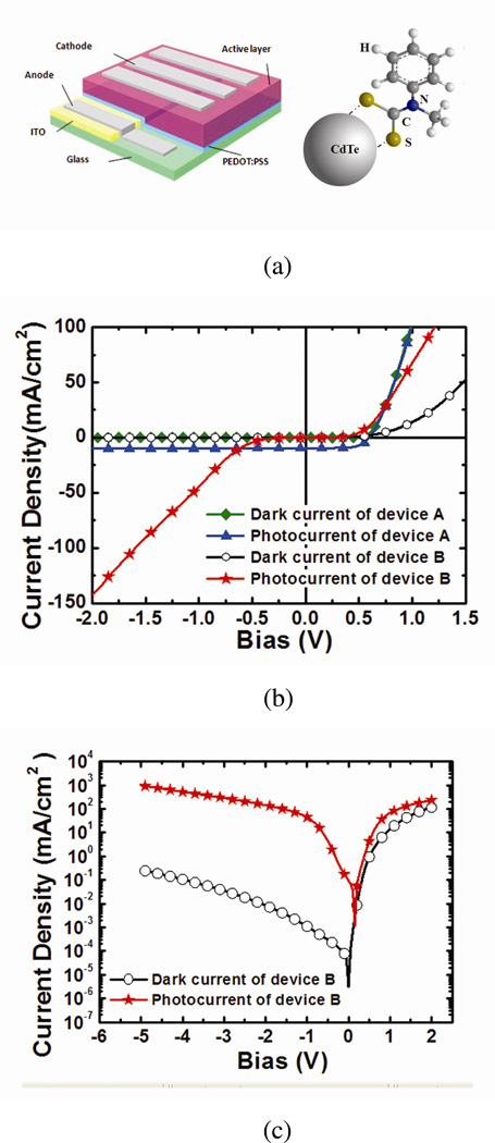
In our system, a P3HT(poly(3-hexylthiophene)):PCBM((6,6)-phenyl-C61-butyric acid methyl ester) polymer matrix film is doped with CdTe NPs, which are capped with N-phenyl-N’-methyldithiocarbamate (PMDTC) (Figure 1 (a)). The CdTe NPs with PMDTC capping ligand are highly soluble in dichlorobenzene (DCB), which also is a good solvent for polymer blends. No NP aggregates are observed, even at a concentration as high as ~30% (300mg/mL) in DCB. Devices made from this polymer/NP blend display high photoconductive gain (EQE~8000%) when the film is reverse-biased at less than −5V. To our knowledge, this is the highest photoconductive gain obtained so far in polymer-based system under such low applied voltages.
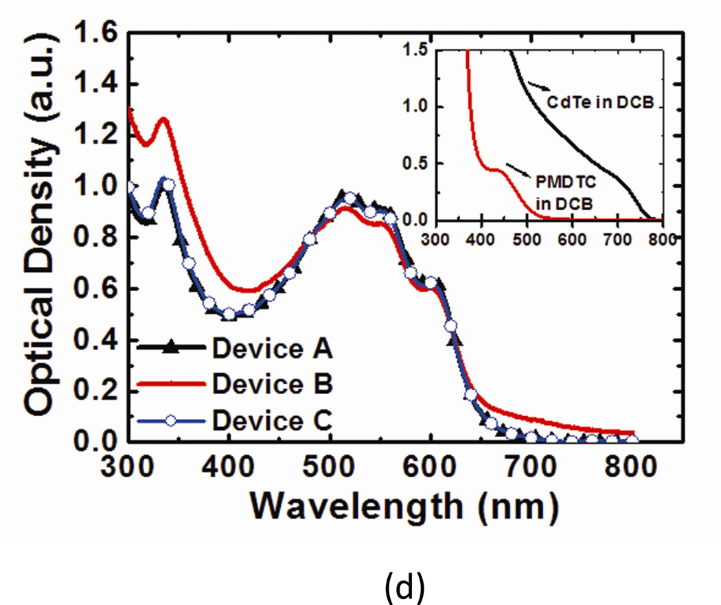
Figure 1. Device structure, current density-voltage (J-V) characteristics, and absorption spectrum.
(a) Device structure and chemical structure of PMDTC ligand (not to scale). (b) The J-V curve of devices A and B. Significant photocurrent increase is observed under reverse bias when CdTe NPs are blended into the P3HT:PCBM matrix. (c) The J-V curve of device B in logarithmic scale. Clear diode characteristic is shown by the dark current density curve. (d) Absorption spectrum of films in devices A, B, and C. PMDTC blended with P3HT:PCBM shows no obvious change in absorption. Inset: Absorption spectrum of CdTe NPs (with PMDTC capping ligands) and free PMDTC in DCB.
All devices reported in this manuscript are of the structure shown in Fig. 1(a) where the active layer is composed of P3HT:PCBM with (device B, B2, and B3) or without (device A) CdTe NPs. Solutions and devices investigated are listed in Table 1. (see Methods for processing details). The current density-voltage (J-V) characteristics of devices A and B are shown in Figure 1(b). While device A shows typical polymer solar cell characteristics12, the dark current of device B in the forward bias region is significantly suppressed, although a clear diode characteristic is still observed (Figure 1(c)). The photovoltaic property almost disappears, but with a higher applied voltage in reverse bias, the photocurrent of device B changes sharply to a much higher value than device A. A reverse bias photocurrent density as high as 952 mA/cm2 is observed at −5V.
Table 1.
List of solutions and devices with detail conditions.
| Solutions | Contents | Solvent |
|---|---|---|
| Solution A | 2% (20mg/mL) P3HT:PCBM (1:1 wt ratio) | DCB |
| Solution B | 2% (20mg/mL) P3HT:PCBM (1:1 wt ratio) with 3.1% (31 mg/mL) CdTe NPs | DCB |
| Solution C | 2% (20mg/mL) P3HT:PCBM (1:1 wt ratio) with 2.2% (22 mg/mL) PMDTC | DCB |
| Devices | Solution used | Solvent annealed* | Cathode | Processing details |
|---|---|---|---|---|
| Device A | Solution A | Yes | Ca/Al | *please see below description |
| Device B | Solution B | Yes | Ca/Al | |
| Device C | Solution C | Yes | Ca/Al | |
| Device B2 | Solution B | No | Ca/Al | Spin coated at 800 rpm for 95seconds |
| Device B3 | Solution B | Yes | MoO3(5nm)/Al(70nm) |
Note: solvent annealing is done by spin-coating the polymer solutions at 800 rpm for 45 seconds and allowing the film to dry slowly in a covered petri-dish until the color of the polymer films change from orange to deep purple.
Absorption spectra of the polymer films in device A, B and C are shown in Figure 1(d), with the absorption of CdTe NPs and PMDTC in DCB shown in the inset. For direct comparison, films used for absorption measurements are controlled to about the same thickness. No obvious absorption change is observed when PMDTC is blended with P3HT:PCBM (device A and C) while increased absorption for wavelengths longer than 650 nm and shorter than 450 nm are observed in device B. Other measurements of device C that are done to exclude the possible contribution of PMDTC to the photoconductive gain are included in supplementary information.
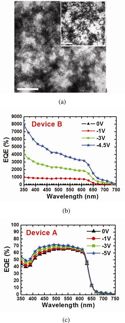
The three vibronic shoulders (at ~515, 550, and 610 nm) which represent strong interchain-interlayer interactions of P3HT12,20, are preserved in the absorption spectra after blending in CdTe NPs. This implies the high concentration CdTe NPs does not hinder the stacking of P3HT under solvent annealing, which is important for high carrier mobility21. Transmission electron microscopy (TEM) images of the film (Figure 2(a)) represent highly condensed aggregates of CdTe NPs. It is worth mentioning that these aggregates have thread-like features (inset of Figure 2(a)) which have not been observed in previously reported TEM images of NPs with other capping ligands in polymer films3,10,22.
Figure 2. TEM images and external quantum efficiency.
(a) TEM images of P3HT:PCBM/CdTe NPs (~3.1% (31mg/mL)) film. Scale bar in the major image is 200 nm and is 1´m for the inset. The solution was drop cast on a TEM grid for sample preparation. Highly condensed aggregates of CdTe NPs are observed and thread-like features are clearly visible in the inset. (b) EQE of device B under zero and reverse bias. Higher than 100% EQE is obtained under reverse bias, even at the absorption edge of CdTe NPs (~700 nm). (c) EQE of device A measured under the same conditions.
The EQE of device B at different wavelengths is shown in Figure 2(b). Higher than 100% EQE is observed at an applied voltage of only −1V. With increasing negative bias, EQEs as high as ~8000% at 350nm and ~600% at 700nm are reached at −4.5V. An EQE higher than 100% implies that extra charges are generated in the devices. In this system, these extra charges are likely to be injected from the external circuit. The possibility of multiple excitons23 generation by one photon is rather low since the photonic energy is not high enough for this process7. The EQE of device A measured under the same conditions is shown in Figure 2(c) for comparison.
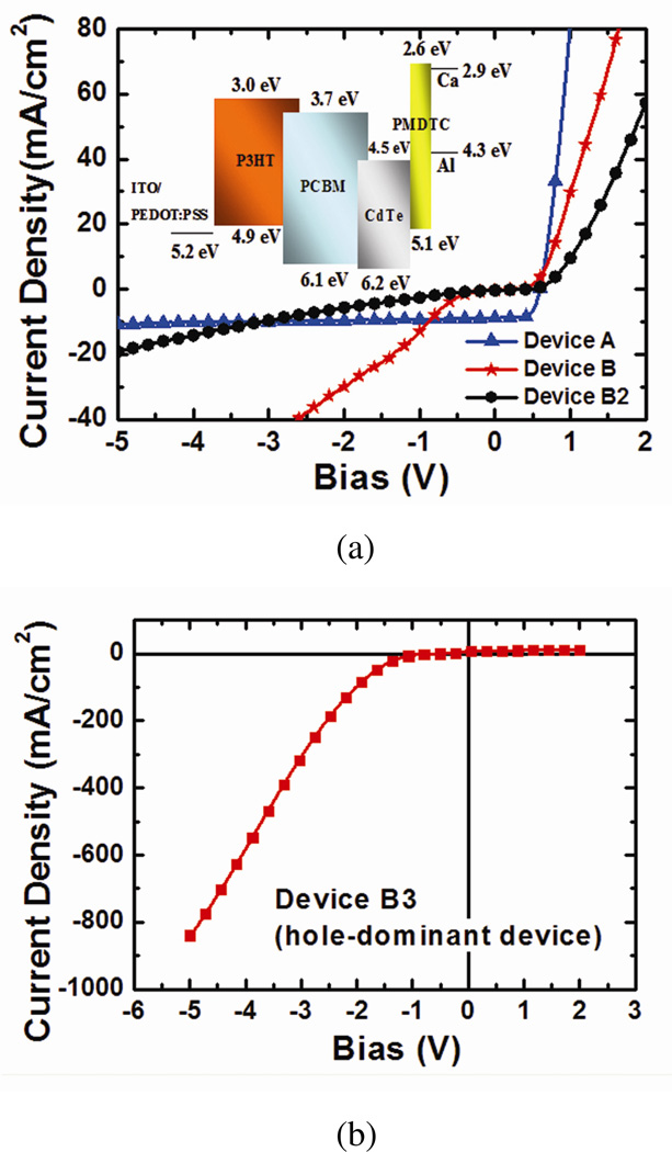
The relative energy levels of P3HT, PCBM and PMDTC have been determined by cyclic voltammetry and are drawn in the inset of Figure 3(a). For the CdTe core, we used the values calculated by Dayal et al.24 for the CdTe NPs of about the same size (~8 nm diameter). Note that the electron affinity of CdTe NPs likely differs based on different preparation methods. Recently, it has been found that the measured energy level of nanocrystals varies significantly with different surface capping group25. To remove the surface ligand effect, here we instead use a calculated value24 for the CdTe core. According to this energy diagram, CdTe NPs act as deep electron traps in this system. Under exposure to light, excitons are generated in CdTe NPs when the wavelength is shorter than its absorption edge, ~750nm. From the relative energy level, the exciton generated at the core of NPs may lose its hole to the PMDTC ligand. This scenario agrees with the observed absence of CdTe NP photoluminescence (PL) in DCB when the capping ligand was changed from oleic acid to PMDTC.
Figure 3. Photocurrent density-voltage characteristic of different devices.
(a) J-V curve of device A, B, and B2 (without solvent annealing). Much higher photocurrent density in reverse bias is observed for device B while the increase of photocurrent density is much slower in device B2. Inset: Relative energy diagram of all the materials used in this manuscript. (b) J-V curve of device B3 (after solvent annealing, hole-dominant device, with MoO3(5nm)/Al(70nm) electrode) under light exposure. A much higher photocurrent density is observed under reverse bias (while MoO3/Al electrode is positively biased).
We thus speculate that the ability of CdTe NPs to trap electrons under illumination leads to photo-induced carrier injection from the cathode, which results in the measured EQE of much higher than 100%. To clarify the role of CdTe NPs, we made another device, device B2 (same as device B, but without solvent annealing, see Table 1). The J-V curve of device B2 is compared with devices A and B in Figure 3(a). The photocurrent of device B2 under reverse bias is much lower than that of device B. This data suggests that the morphology of the polymer/NP system is also significant for this high photoconductive gain, and is not simply due to the addition of CdTe NPs. Note that from the J-V curve of device B2, a photoconductive gain is expected only when higher bias is applied. A similar phenomenon has been observed by Campbell et al19 recently. In their work, PbSe quantum dots and PCBM were blended with polymer, respectively, and the conductive gain is obtained in both systems under higher reverse bias. The photoconductive gain is attributed to the photo-generated electrons being trapped by either PbSe quantum dots or PCBM in the bulk, which caused the injection of hole carriers from the external circuit.
To better understand the function of solvent annealing in our system, a hole-dominant device (device B3, see Table 1) is studied. In our devices, forward bias is defined as ITO positively biased and vice versa. Under reverse bias, holes are injected from MoO3/Al electrode of device B3. A photocurrent density of 838 mA/cm2 was observed at −5V, which is much higher than that under forward bias. (Figure 3(b)). The much higher hole injection from MoO3/Al to the polymer blend implies that the injection barrier between the MoO3/Al electrode and the polymer blend is much lower than that of the ITO(PEDOT)/polymer contact. Devices without CdTe NPs are made simultaneously with the same conditions but no similar phenomenon is observed.
The much higher photocurrent of device B3 in reverse bias than in forward bias also implies that the distribution of CdTe NPs along the direction normal to the film may not be uniform, i.e. the concentration may be higher near the polymer blend/MoO3 interface, which lowers the injection barrier for holes injected from MoO3 into the polymer blend layer. Similar aggregation of NPs on the top of polymer films has also been observed in polymer light-emitting diodes26. For comparison, a hole-dominant device made without solvent annealing does not show similar effect and the J-V curve looks symmetric. According to these observations, it is very likely that the concentration of CdTe NPs is higher near the polymer blend/MoO3 interface as a result of solvent annealing.
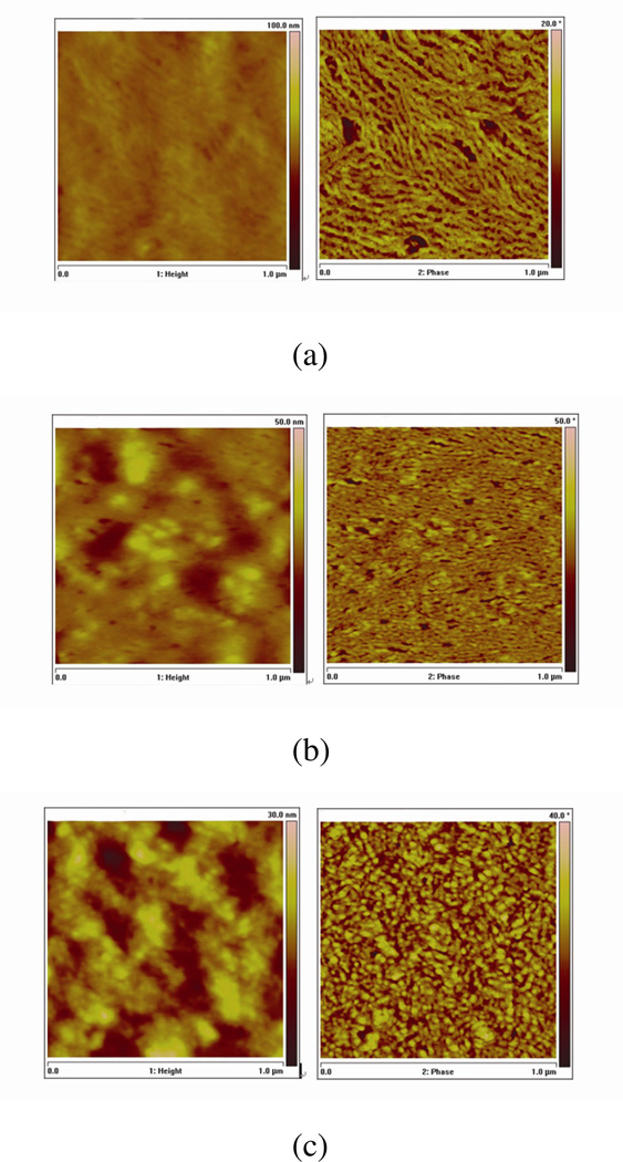
Tapping-mode atomic force microscopy is used to further study the surface topography and phase images of A, B and B2 films (Figure 4(a), (b), and (c)), which normally are in direct contact with cathodes (Ca/Al or MoO3/Al) in devices. Long fibrillar structures are clearly observed in the phase image of the polymer film in device A (Figure 4(a), right) while the film in device B2 (Figure 4(b), right) represents a similar structure but with shorter and less ordered fibrillar segments. This fibrillar structure represents the crystalline domains of P3HT12. However, the film in device B provides a very different phase image (Figure 4(c), right); island-like structures appear instead of fibirillar features. These images show that surface morphology change is a result of adding NPs coupled with the solvent annealing process. The concentration of CdTe NPs near the top of the polymer blend film is likely higher, yielding a totally different morphology.
Figure 4. Tapping mode atomic force microscopy images of the polymer films.
Topography (left) and phase images (right) of device A, B2, and B in 1´m are shown in (a), (b), and (c), respectively. The phase images of devices A and B2 show filbrillar structure while device B represents an island-like surface morphology. The absence of fibrillar structure in the surface morphology of device B is a result of adding NPs coupled with solvent annealing process.
To conclude, a solvent annealing step after film spin coating likely gives rise to a higher concentration of CdTe NPs on the top of the annealed film. Under light exposure, CdTe NPs with photo-induced trapped electrons thus lower the hole injection barrier from the top electrode to the P3HT film. Therefore, CdTe NPs behave as a valve that controls the hole injection under reverse bias. The contribution to the photoconductive gain can be from both the NPs near the top surface of the polymer film and in the bulk19. Judging from our data, NPs near the top surface might play a dominant role. A higher than 100% EQE at the absorption edge of CdTe NPs (~700 nm) suggests that significant charge injection already occurs. At the onset of P3HT absorption (~650 nm), more excited electrons are generated in P3HT, resulting in more electrons being trapped in the NPs and thus an even higher charge injection rate. With this polymer/NP blend system, a high photoconductive gain can be obtained over the absorption range of the polymer and NPs.
Methods
Experimental
Solution preparation
Solution A consists of 2% (20 mg/mL) P3HT:PCBM (1:1 weight ratio) in dichlorobenzene (DCB) solvent. Solution B was made by mixing P3HT:PCBM solution with CdTe NPs and the concentration of CdTe NPs after mixing is ~3.1% (31mg/mL). Solution C is made by mixing P3HT:PCBM solution and PMDTC and the concentration of PMDTC after mixing is ~2.2% (22mg/mL). The concentration of P3HT and PCBM were kept as 2% in solution B and C after mixing.
Device Fabrication
Devices A, B, and C were made from solutions A, B, and C, respectively. All the devices are of the structure of indium tin oxide(ITO)/PEDOT:PSS/polymer blend/Calcium(Ca)/Aluminum(Al) except device B3. PEDOT:PSS is poly(ethylenedioxythiophene):polystyrene sulfonate. A PEDOT:PSS layer was pre-coated onto the ITO substrate before spin-casting the solutions. All solutions were spin-coated at 800rpm for 45 seconds. The thickness of the polymer films, measured with a Dektak 3030 profilometer, for devices A, B, and C were ca. 215 nm, 255 nm, and 225 nm, respectively. After spin-coating, the wet polymer films were left to dry slowly in petri dishes until the color of the polymer films changed from orange to purple. This slow growth (or solvent annealing) process was demonstrated by Li et al12. to achieve an optimized morphology for solar cell devices. Thermal annealing at 110°C for 10 minutes was then applied to device A before deposition of electrodes from evaporated metal. A bilayer cathode consisting of a calcium layer (20 nm) and subsequently an aluminum layer (100 nm) was deposited by thermal evaporation under vacuum (1x10⁻⁶ torr). The active area for all the devices discussed here was ~12 mm2. Device B2 was made by spin-coating solution B at 800 rpm for 95 sec to ensure the film was dry (the color of the polymer film does not change with time after spin-coating).
Experiment conditions
The current density-voltage (J-V) characteristics were measured using a Keithley 2400 source-measure unit. A calibrated solar simulator (Oriel) with 100 mW/cm2 power density was used as the light source. In addition, the external quantum efficiency (EQE) was used to determine the device photo response as a function of wavelength. EQE is defined as the number of charge carriers collected per incident photon at a specific wavelength. In the EQE measurement, a xenon lamp (Oriel, model 66150, 75W) was used as light source; and a chopper and lock-in amplifier were used for phase sensitive detection. The wavelength was controlled by a monochrometer. To ensure an accurate counting of incident photons, a calibrated Si photodiode was used as a reference device.
Supplementary Material
Acknowledgements
H.-Y. Chen and Y. Yang acknowledge the financial support from Solarmer Energy Inc. (grant number 20061880) and the Air Force Office of Scientific Research (FA9550-07-1-0264). The help from Mr. Hyun Cheol Lee for TEM images and the valuable discussion with Dr. Gang Li in Solarmer Energy Inc. are also highly appreciated. H.-Y. Chen is grateful to Mr. Wei Lek Kwan and Bao Lei for helping the transient measurement.
Footnotes
Author contributions
H.–Y. Chen conceived and performed the experiments and measurement. Michael K. F. Lo performed CdTe NPs and capping ligand synthesis. G. Yang performed the AFM images. H. G. Monbouquette and Y. Yang conceptualized and directed the research project. All authors discussed the results and commented on the manuscript.
Competing financial interests
The authors declare that they have no competing financial interests.
References
- 1.Huynh WU, Dittmer JJ, Alivisatos AP. Hybrid nanorod-polymer solar cells. Science. 2002;295:2425. doi: 10.1126/science.1069156. [DOI] [PubMed] [Google Scholar]
- 2.Sun B, Greenham NC. Improved efficiency of photovoltaics based on CdSe nanorods and poly(3-hexylthiophene) nanofibers. Phys. Chem. Chem. Phys. 2006;8:3557. doi: 10.1039/b604734n. [DOI] [PubMed] [Google Scholar]
- 3.Han L, et al. Synthesis of high quality zinc-blende CdSe nanocrystals and their application in hybrid solar cells. Nanotechnology. 2006;17:4736. doi: 10.1088/0957-4484/17/18/035. [DOI] [PubMed] [Google Scholar]
- 4.Zhou Y, et al. Hybrid nanocrystal/polymer solar cells based on tetrapod-shaped CdSexTe1-x nanocrystals. Nanotechnology. 2006;17:4041. doi: 10.1088/0957-4484/17/16/008. [DOI] [PubMed] [Google Scholar]
- 5.Beek WJE, Wienk MM, Janssen RAJ. Efficient hybrid solar cells from zinc oxide nanoparticles and a conjugated polymer. Adv. Mater. 2004;16:1009. [Google Scholar]
- 6.Mcdonald SA, et al. Solution-processed PbS quantum dot infrared photodetectors and photovoltaics. Nature Mater. 2005;4:138. doi: 10.1038/nmat1299. [DOI] [PubMed] [Google Scholar]
- 7.Qi D, Fischbein M, Drndic M, Selmic S. Efficient polymer-nanocrystal quantum-dot photodetectors. Appl. Phys. Lett. 2005;86:093103. [Google Scholar]
- 8.Cui D, Xu J, Zhu T, Paradee G, Ashok S. Harvest of near infrared light in PbSe nanocrystal-polymer hybrid photovoltaic cells. Appl. Phys. Lett. 2006;88:183111. [Google Scholar]
- 9.Choudhury KR, Sahoo Y, Ohulchanskyy TY, Prasad PN. Efficient photoconductive devices at infrared wavelengths using quantum dot-polymer nanocomposites. Appl. Phys. Lett. 2005;87:073110. [Google Scholar]
- 10.Greenham NC, Peng X, Alivisatos AP. Charge separation and transport in conjugated-polymer semiconductor-nanocrystal composites studied by photoluminescence quenching and photoconductivity. Phy. Rev. B. 1996;54:17628. doi: 10.1103/physrevb.54.17628. [DOI] [PubMed] [Google Scholar]
- 11.Huynh WU, Dittmer JJ, Libby WC, Whiting GL, Alivisatos AP. Controlling the morphology of nanocrystal-polymer composites for solar cells. Adv. Funct. Mater. 2003;13:73. [Google Scholar]
- 12.Li G, et al. “Solvent Annealing” effect in polymer solar cells based on poly(3-hexylthiophene) and methanofullerenes. Adv. Funct. Mater. 2007;17:1636. [Google Scholar]
- 13.Sze SM. Physics of semiconductor devices. Wiley: New York; 1981. [Google Scholar]
- 14.Caserta G, Rispoli B, Serra A. Space-charge-limited current and band structure in amorphous organic films. Phys. Stat. Sol. 1969;35:237. [Google Scholar]
- 15.Hiramoto M, Imahigashi T, Yokoyama M. Photocurrent multiplication in organic pigment films. Appl. Phys. Lett. 1994;64:187. [Google Scholar]
- 16.Reynaert J, Arkhipov VI, Heremans P, Poortmans J. Photomultiplication in disordered unipolar organic materials. Adv. Funct. Mater. 2006;16:784. [Google Scholar]
- 17.Marks RN, Halls JJM, Bradley DDC, Friend RH, Holmes AB. The photovoltaic response in poly(p-phenylene vinylene) thin film devices. J. Phys. Condens. Matter. 1994;6:1379. [Google Scholar]
- 18.Daubler TK, Neher D. Efficient bulk photogeneration of charge carriers and photoconductivity gain in arylamino-PPV polymer sandwich cells. Phys. Rev. B. 1999;59:1964. [Google Scholar]
- 19.Campbell IH, Crone BK. Bulk photoconductive gain in poly(phenylene vinylene) based diodes. J. Appl. Phys. 2007;101:024502. [Google Scholar]
- 20.Sirringhaus H, et al. Two-dimensional charge transport in self-organized, high-mobility conjugated polymers. Nature. 1999;401:685. [Google Scholar]
- 21.Li G, et al. High-efficiency solution processable polymer photovoltaic cells by self-organization of polymer blends. Nature Mater. 2005;4:864. [Google Scholar]
- 22.Choi SH, et al. Synthesis of size-controlled CdSe quantum dots and characterization of CdSe-conjugated polymer blends for hybrid solar cells. J. photochem. and photobiol A: Chemistry. 2006;179:135. [Google Scholar]
- 23.Schaller RD, Agranovich VM, Klimov VI. High-efficiency carrier multiplication through direct photogeneration of multi-excitons via virtual single-exciton states. Nature Physics. 2005;1:189. [Google Scholar]
- 24.Dayal PB, Mehta BR, Paulson PD. Spin-orbit splitting and critical point energy at Γ and L points of cubic CdTe nanoparticles: effect of size and nonspherical shape. Phys. Rev. B. 2005;72:115413. [Google Scholar]
- 25.Soreni-Harari M, et al. Tuning energetic levels in nanocrystal quantum dots through surface manipulations. Nano Lett. 2008;8:678. doi: 10.1021/nl0732171. [DOI] [PubMed] [Google Scholar]
- 26.Coe S, Woo W, Bawendi M, Bulovic V. Electroluminescence from single monolayers of nanocrystals in molecular organic devices. Nature. 2002;420:800. doi: 10.1038/nature01217. [DOI] [PubMed] [Google Scholar]
Associated Data
This section collects any data citations, data availability statements, or supplementary materials included in this article.


