Abstract
Cracking in Silicon solar cells is an important factor for the electrical power-loss of photovoltaic modules. Simple geometrical criteria identifying the amount of inactive cell areas depending on the position of cracks with respect to the main electric conductors have been proposed in the literature to predict worst case scenarios. Here we present an experimental study based on the electroluminescence (EL) technique showing that crack propagation in monocrystalline Silicon cells embedded in photovoltaic (PV) modules is a much more complex phenomenon. In spite of the very brittle nature of Silicon, due to the action of the encapsulating polymer and residual thermo-elastic stresses, cracked regions can recover the electric conductivity during mechanical unloading due to crack closure. During cyclic bending, fatigue degradation is reported. This pinpoints the importance of reducing cyclic stresses caused by vibrations due to transportation and use, in order to limit the effect of cracking in Silicon cells.
PV modules are supposed to have a lifetime longer than 20 years under the exposure to environmental conditions. Thermo-mechanical loads induce stresses into the components of the module, especially into the crystalline Silicon (Si) solar cells, which are affected by cracking1,2,3,4,5,6,7,8,9. The Institute for Solar Energy Research Hamelin and TÜV Rheinland provided detailed reports on PV modules quality during the period 2008–201110. The percentage of cracked cells in modules as delivered before their installation in the field was 6%, presumably related to vibrations and impacts during transportation. Then, ageing effects due to environmental conditions such as snow, wind gusts, hail and rapid temperature variations are responsible for further propagation of cracks11, although it is nearly impossible to assess the individual contribution of each factor. Analysis and statistics of degradation mechanisms in Silicon modules observed in the field have reported various sources of failure of PV modules, namely: laminate internal electric circuit failure, glass breakage, junction box or cables failure, encapsulant decoloration or backsheet debonding, cell failures due to cracking. Among them, cell failure is considered to be responsible for 10% of the totally observed PV module failures, with an occurrence analogous to that of junction box or cables failure and to encapsulant decoloration or backsheet debonding12.
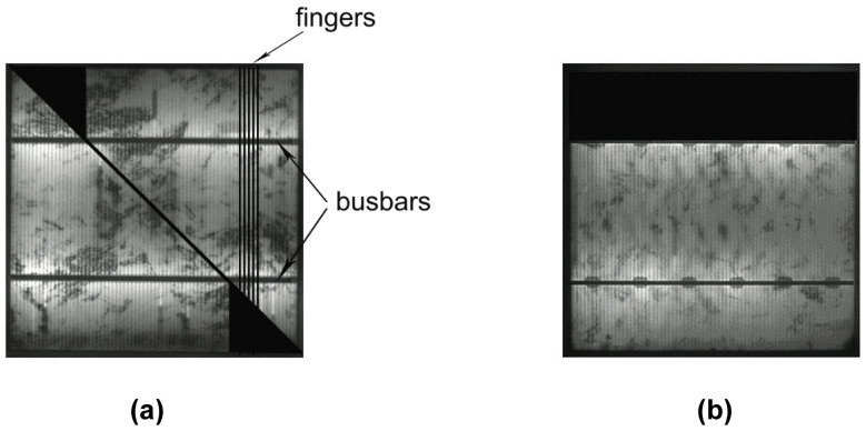
Cracks on the millimetre or centimetre size are mostly invisible by naked eye but they can be localized according to the EL technique13. Such cracks can lead to electrically inactive cell areas thus reducing the power output of the module and the fill factor14. This takes place via the following mechanisms, i.e.: a linear decreasing of the short circuit current by increasing the inactive cell area3,15,16, and an increase in the series resistance of the cell due to cracking3,5. For instance, experimental results5 have shown an increase in the series resistance of the cell of about 7% due to cracking with a corresponding power-loss of 4% and a fill factor reduction of 3%. Other experimental investigations3 have shown that cracks inserted in solar cells by the application of a uniform pressure to simulate snow can lead up to 1.5% of power loss. After the subsequent application of 200 humidity freeze cycles according to standard specifications17, such cracks propagate, the electrically disconnected areas increase in size and up to 10% of power loss has been reported. Potentially, if a crack crossing an Aluminium conductor (called finger) is sufficiently open, then the finger may fail and the electric flow to the busbar in case of normal operating condition, or from the busbar in case of forward bias condition as in the EL testing, would be interrupted. Therefore, portions of Si cells can be potentially deactivated by cracks and their impact on power-loss reasonably depends on their inclination and position with respect to the busbars, see Figs. 1(a) and (b). For instance, a crack parallel to the busbar on the upper side of the cell could lead up to 25% of electrically inactive area (Fig. 1(b)). According to this pure geometrical criterion which does not take into account neither physical mechanisms such as thermo-mechanical deformation, nor the fact that the cells are embedded in the composite PV module, worst-case scenarios have been predicted by considering all the experimentally detected3 or numerically simulated8 cracks as perfectly insulated lines.
Figure 1. Geometrical criterion showing the expected amount of potentially inactive cell areas depending on the orientation of the crack with respect to the busbars3,8: 6% of potentially inactive cell (a); 25% of potentially inactive cell (b).
In reality, it is reasonable to expect intermediate configurations where cracks may partially conduct depending on the relative crack opening displacement at crack faces. A complete modelling of the phenomenon should therefore consider the following steps: (i) simulation of crack nucleation and propagation according to a computational approach based on the cohesive zone model (CZM)18,19,20, where cohesive tractions opposing to the relative displacements of the crack faces are decreasing functions of opening and sliding; (ii) analysis of thermal effects by augmenting the basic mechanical CZM to take into account the additional thermal resistance of cracks9; (iii) modelling of the electric response of the cell. For this last item, localized series resistances dependent on crack opening might be postulated in correspondence of cracks, in addition to the distributed series resistance. A preliminary experimental observation supporting coupling effects induced by the thermo-mechanical field on the electric one due to cracking regards the highly oscillating electrical response in time of a PV string containing a cracked cell, depending on the cell temperature7.
At present, electric models of solar cells do not consider this form of coupling induced by cracking. In the most refined versions21,22, a discretization of the solar cell is made in the plane and a two-diode model is applied to each node of the mesh to predict the electric response of the semiconductor. In case of hot spots, however, it was indeed necessary to modify the value of the series resistance in the nodes close to a crack. Hence, to achieve a predictive stage useful for power-loss predictions and durability assessment of PV systems exposed to environmental loads, series resistance values used as input of the circuit model should be related to the thermo-elastic stress state in the solar cell.
Results
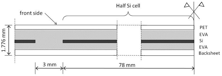
To make an insight into the mechanisms leading to these coupling effects, a bending test on a rectangular PV module has been performed in the laboratory by monitoring cracking at different deformation levels by EL imaging. A semi-flexible module made of 2 rows of 5 monocrystalline Si cells each is used. The dimension of the cells is 156 × 156 mm. The partially symmetric arrangement of the layers through the thickness (0.265 mm of polyethylene terephthalate, 0.600 mm of epoxy-vinyl-acetate, 0.166 mm of Silicon, 0.400 mm of epoxy-vinyl-acetate and 0.345 mm of backsheet) and the different Young moduli of the materials lead to Si cells just above the neutral axis of the cross-section (see Fig. 2). This type of module, which has a certain degree of flexibility, can be used in many applications where the substrate we would like to bond the module is curved. In order to induce a tensile stress state inside solar cells, the curvature imposed to the module is such that the convex side after bending corresponds to the PET side (front side in Fig. 2).
Figure 2. Sketch of the cross-section of the PV module near the symmetry line.
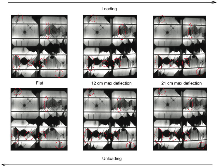
To create pre-existing cracks and study their evolution depending on the imposed flexure, moderate impacts have been made with PMMA balls of 4 cm of diameter at a velocity of 6 m/s. In this way, cracks are introduced by an indentation effect. The EL images of four solar cells in the middle of the panel are shown in Fig. 3.
Figure 3. Evolution of EL signal during bending loading and unloading for different deflections.
Location of impacts can be clearly distinguished by the circular dark spots from where diagonal cracks, influenced by the crystallographic planes of cubic face centred monocrystalline Silicon, depart. These patterns are completely invisible by naked eye and can only be determined by the EL technique. In some cases, large electrically insulated cell portions, appearing as dark areas, are present. Other portions, circled with dashed lines, show regions isolated by cracks but still partially conducting from the electrical point of view. This can be well explained by the assumption that their crack opening is smaller than a critical value for complete electric insulation and by a compressive stress state inside the cells due to residual thermo-elastic stresses induced by cooling down the module from the lamination temperature at 150°C to the ambient temperature at 20°C.
To assess the residual stress and deformation states inside the PV module, a 2D plain strain finite element (FE) model of the layered composite in the plane of bending has been analyzed using the Finite Element Analysis Programme FEAP23. Taking advantage of the structural symmetry, one half of the module has been analyzed by introducing symmetry boundary conditions on the symmetry line. The opposite edge of the module is simply supported in the direction orthogonal to the longitudinal axis. The thermal expansion coefficients of the plastic layers, EVA and Silicon are, respectively, α = 5.04 × 10⁻⁵, 2.70 × 10⁻⁴ and 2.49 × 10⁻⁶. The other elastic parameters are as in Ref. 24. Due to its thermo-visco-elastic behaviour, a Young modulus of EVA equal to 1 MPa has been selected, which is the lowest value in the considered range of temperatures according to experimental results24. In any case, a possible variation of the Young modulus of EVA from 1 to 10 MPa is inducing an increase of about 10% in the compressive stresses inside Silicon. The FE computations estimate a compressive stress field in the Si cells variable from 0 MPa at their borders up to 60 MPa in their centre (see the contour plot in Fig. 4). Therefore, this residual stress field is beneficial for the module since any initial crack or defect present in Silicon would be closed by compression.
Figure 4. Contour plot of the horizontal stresses inside the PV laminate in the portion near the symmetry line.
By increasing the mid-span bending deflection (upper row in Fig. 3, loading direction from left to right), cracks open and additional insulated dark areas appear, thus confirming that the electrical behaviour of cracks does depend on the elastic deformation. Very interesting is the unloading stage (lower row in Fig. 3, unloading direction from right to left), where cracks come into contact and conduct again. Hence, although globally the amount of damage is increased during the cycle since the final EL image is more dark than before, an electric recovery due to crack closure is reported.
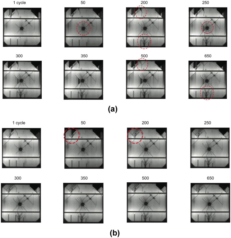
The evolution of degradation by increasing the amount of bending cycles (from zero to a maximum mid-span deflection of 21 cm per cycle) has also been monitored and it is shown in Fig. 5(a), where EL images of a significant cell of the module have been recorded at the point of maximum deflection for 1, 50, 200, 250, 300, 350, 500 and 650 cycles. The cyclic tests have been conducted in the ambient temperature (20°C). Regarding the EL measurement procedure, to minimize localized heating effects in the cells, the total time of application of the external voltage was 30 s (see Methods). From the time of switching the power supplier on to its switching off, six EL images have been recorded to monitor this transient regime. During that, no crack propagation was observed. Therefore, temperature effects can be excluded. Brittle crack propagation due to overloading has also to be excluded. In fact, the force-displacement curve of the panel tested under displacement control was linear elastic over the whole displacement range. This is in line with analogous experimental observations4 regarding glass-laminated mini-modules tested under four-point bending. Moreover, unloading and reloading was taking place along the same curve. This is reasonable since the pre-existing crack pattern due to hail tests is slightly changing from cycle to cycle and it does not significantly affect the overall stiffness of the module. On the other hand, the effect of the crack pattern regards the electric response, as shown by comparing the EL images at different cycles.
Figure 5. Fatigue degradation of the electric response and increasing crack pattern at different bending cycles.
EL images are taken at the maximum deflection point of the module (δ = 21 cm) (a) and at the unloaded configuration (δ = 0 cm) (b).
During the first 50 cycles we report a propagation of cracks around the dark central point of impact. Crack propagation further takes place from 50 to 200 cycles, with the appearance of new cracks from the lower border of the cell, originating from an edge crack. No crack propagation takes place from 200 to 250 cycles, although the EL intensity between diagonal cracks diminishes, thus implying a material degradation and a reduction of electric conductivity across the cracks. This trend continues further by increasing the number of cycles, with also further crack propagation (cycle 300) and coalescence of two propagating cracks (cycle 350). At 500 cycles, a new crack is originated from an initial one on the upper side of the cell as a result of a crack-branching mechanism. After the appearance of this new crack, the dark EL area just on the left of it becomes conductive again. This can be explained as the effect of the phenomenon of strain localization, frequently observed in brittle materials, which corresponds to a stress relief in the surrounding cracks when a major crack propagates18. Therefore, with the appearance of a new crack, the previous one in the surrounding is relaxed and it experiences a reduction of its relative opening displacement.
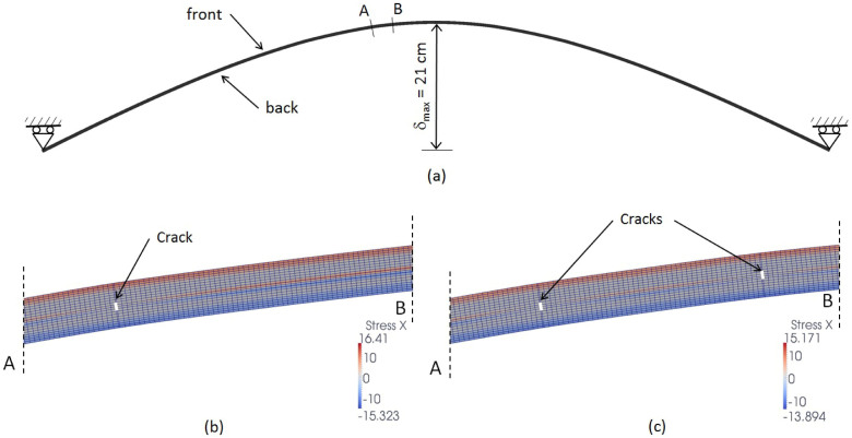
To confirm the effect of a new crack on the crack opening of a pre-existing crack in case of a brittle material embedded in the laminate, a FE study based on nonlinear fracture mechanics is proposed. For more details about the CZM, see Ref. 9. In the 2D approximation of the PV module shown in Fig. 6(a), one or two cohesive cracks (distant 0.9 cm from each other) are introduced in the Si cell placed near the symmetry line (see Figs. 6(b) and 6(c)). In the numerical simulations, the PV module is loaded by imposing a displacement to the middle cross-section up to δmax = 21 cm as shown in Fig. 6(a). Residual thermo-elastic stresses are not considered here for the sake of simplicity. If the stress relief takes place, then it would happen also in the presence of residual thermo-elastic stresses. A very low cohesive peak stress of σmax = 0.2 MPa is considered to simulate a very low cohesion due to a severe state of damage. The contour plots of the horizontal stress field superimposed to the deformed meshes of the portion of the module where cracks are placed are shown in Figs. 6(b) and 6(c). Stresses are slightly reduced by the simultaneous presence of two cracks and the crack opening of the pre-existing crack reduces from 11 μm to 9 μm. Therefore, the effect of strain localization induced by the propagation of new cracks supports the hypothesis of unloading effects at pre-existing cracks that might come into contact, thus leading to a recovery of their electric conductivity.
Figure 6. Structural scheme (a); contour plot of the horizontal stress field in case of one single crack (b); contour plot of the horizontal stress field in case of two cracks (c).
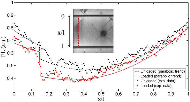
The phenomenon of electric recovery due to crack closure already noticed in the case of the first cycle can be observed also after several cycles. For instance, comparing the EL data along a cross-section perpendicular to the busbars and passing through a crack in the loaded and unloaded configurations for 50 cycles (Figs. 5(a) and (b)), we obtain the diagram in Fig. 7. Values of EL close to unity correspond to very bright Si areas, whereas values close to zero are dark “electrically inactive” zones. As visually emphasized by the superimposed parabolic trend with a discontinuity of first type in correspondence of the crack (x/l = 0.15), a jump in the EL data takes place and it is higher for the configuration at maximum deflection where the crack opening is reasonably larger.
Figure 7. EL data along a cross-section passing through a crack for 50 cycles in the loaded and unloaded configurations.
Finally, strain-localization can be evidenced again by comparing in Fig. 5(b) EL images for 50 and 200 cycles, see the circled areas. The propagation of a diagonal crack to the left relieves the deformation in the Si area, the diagonal crack on the right experiences a reduction in crack opening and the EL image of Silicon above becomes brighter.
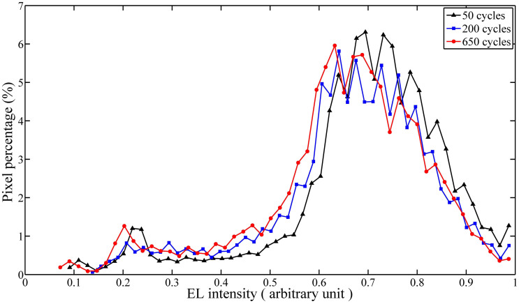
A quantitative analysis of EL images at maximum deflection (Fig. 5(a)) shows that the statistical distribution of pixels having a given EL intensity is particularly skew-symmetric, with a long tail for EL intensities less than 0.5 (Fig. 8). Moreover, although the difference between EL images by increasing the number of cycles is apparently marginal, i.e., only a few cracks propagate and some regions become darker, the EL distributions quantify the fatigue degradation trend. By increasing the number of cycles, in fact, the EL distribution shifts to the left. For high EL intensities, the pixel percentage is diminished by increasing the number of cycles. Exactly the opposite trend takes place in the low EL intensity range, i.e., more pixels become darker.
Figure 8. EL distributions for different number of bending cycles at maximum deflection.
Note the shift of the distributions to the left by increasing the number of cycles, a trend consistent with the progression of fatigue degradation.
Conclusions
The experimental results communicated in this study show that, due to the encapsulation of Si cells into a ductile viscoelastic polymeric material, coupling between the electric response measured by EL images and the elastic deformation takes place due to cracking. Therefore, the worst case scenario consisting in all the detected cracks as perfectly insulated ones has to be considered with care, since more complex degradation phenomena occur in reality. In particular, we have shown the appearance of electrical recovery due to crack closure and residual thermo-elastic stresses, fatigue degradation, crack branching and crack coalescence, stress relief and recovery in the EL signal in case of strain localization induced by crack propagation of existing cracks or by new crack nucleation. It has to be remarked that all of these phenomena are impossible in stand alone Si cells which are very brittle and display a different behaviour as compared to Silicon at the micro-scale, like that used for MEMS25. Therefore, modelling of Si solar cells behaviour by neglecting their embedding in a composite should be done with care in case of PV applications. The creation of mechanical defects and its effect on the solar cell performance is also relevant for thin film solar cells15,16,26. In these and in the present cases, an additional complexity as compared to MEMS is related due to the very different size-scales and thicknesses of the various layers which suggests the use of multi-scale computational strategies to model 3D geometries.
The reported results have general implications for any kind of conductive material embedded in a ductile viscoelastic one, see, e.g., graphene layers dispersed into a polymeric matrix27. In other words, the global behaviour cannot be predicted from the mechanical properties of the individual constituents, but it comes out as the result of the interaction of the system's components, a feature typical of complex systems.
The present results pinpoint the need of modelling thermo-electro-mechanical coupling effects in Si solar cells embedded in PV modules, requiring the development of multidisciplinary research involving electronics, materials science and computational mechanics.
From the industrial and engineering point of views, the present results imply that the quasi-static application of very high distributed pressures as requested by qualification standards11 is not enough if we are interested in evaluating the actual degradation rate and possibly infer about the lifetime of produced PV modules. In fact, other unexpected forms of damage, like fatigue degradation, are indeed possible due to the composite structure of the module and can be induced by very common sub-critical loads like vibrations due to transportation or wind gusts, phenomena not yet characterized so far.
Methods
Electroluminescence (EL) imaging
A detailed evaluation of the amount of damage and cracking in Si cells can be conducted using the EL technique. It is a non-destructive method based on the evaluation of the level of luminescence emitted by Silicon when subjected to an imposed electric potential in forward bias condition. Electrically insulated zones or cracks can be identified by their low EL intensity, thus resulting in less bright images. In the present tests, PV panels are supplied by a 10 A bias DC by the Genesys GENH60-12.5 (750W-1U, TDK Lambda) power supplier. EL emission is detected by the cooled digital 12 bit CCD camera pco.1300 solar, with a resolution of 1392 × 1040 pixel and equipped by the Schneider Kreuznach XNP F1.4 lens with SWIR coating 800–1800 nm. In order to reach a meaningful level of detection it is essential to maintain a high signal to noise ratio, cutting off all possible sources of light. Hence, tests are performed inside a darkroom shading all the possible sources of light to avoid reflection effects. By using nearly the maximum aperture of the camera (F1.8), the focus of the camera has been adjusted during the bending test to obtain perfect focus for all the various deflections of the module. An exposure time of 5 s has been used. A post-processing of the acquired EL images has been made by using the facilities of the software CamWare. In particular, cut-off filters of 600 and 8200 nm have been used for all the images to make them comparable and remove very high and very low emission spectrum frequencies.
Author Contributions
M.P. participated in the design of the experiments, in the analysis of the results and in writing the manuscript. M.C., I.B. and A.I. carried out the experiments in the laboratory and contributed to the manuscript preparation. M.C. carried out the finite element simulations. All authors discussed the results and commented on the manuscript.
Acknowledgments
The research leading to these results has received funding from the European Research Council under the European Union's Seventh Framework Programme (FP/2007–2013)/ERC Grant Agreement No. 306622 (ERC Starting Grant “Multi-field and multi-scale Computational Approach to Design and Durability of PhotoVoltaic Modules” – CA2PVM). The support of the Italian Ministry of Education, University and Research to the Project FIRB 2010 Future in Research “Structural mechanics models for renewable energy applications” (RBFR107AKG) is also gratefully acknowledged.
References
- Kajari-Schröder S., Kunze I., Eitner U. & Köntges M. Spatial and orientational distribution of cracks in crystalline photovoltaic modules generated by mechanical load tests. Sol. Energy Mater. Sol. Cells 95, 3054–3059 (2011). [Google Scholar]
- Kajari-Schröder S., Kunze I. & Köntges M. Criticality of cracks in PV modules. Energy Procedia 27, 658–663 (2012). [Google Scholar]
- Köntges M., Kunze I., Kajari-Schröder S., Breitenmoser X. & Bjrneklett B. The risk of power loss in crystalline silicon based photovoltaic modules due to microcracks. Sol. Energy Mater. Sol. Cells 95, 1131–1137 (2011). [Google Scholar]
- Sander M., Dietrich S., Pander M., Ebert M. & Bagdahn J. Systematic investigation of cracks in encapsulated solar cells after mechanical loading. Sol. Energy Mater. Sol. Cells 111, 82–89 (2013). [Google Scholar]
- Khatri R., Agarwal S., Saha I., Singh S. K. & Kumar B. Study on long term reliability of photo-voltaic modules and analysis of power degradation using accelerated aging tests and electroluminescence technique. Energy Procedia 8, 396–401 (2011). [Google Scholar]
- Munoz M. A., Alonso-Garcia M. C., Vela N. & Chenlo F. Early degradation of silicon PV modules and guaranty conditions. Sol. Energy 85, 2264–2274 (2011). [Google Scholar]
- Weinreich B., Schauer B., Zehner M. & Becker G. Validierung der Vermessung gebrochener Zellen im Feld mittels Leistungs PV-Thermographie. Proc. 27 Symposium Photovoltaische Solarenergie, 190–196 (2012). [Google Scholar]
- Paggi M., Corrado M. & Rodriguez M. A. A multi-physics and multi-scale numerical approach to microcracking and power-loss in photovoltaic modules. Compos. Struct. 95, 630–638 (2013). [Google Scholar]
- Paggi M. & Sapora A. Numerical modelling of microcracking in PV modules induced by thermo-mechanical loads. Energy Procedia 38, 506–515 (2013). [Google Scholar]
- Köntges M., Kajari-Schröder S., Kunze I. & Jahn U. Crack statistics of crystalline silicon photovoltaics modules. 26th European Photovoltaic Solar Energy Conference and Exhibition Hamburg, Germany, September5–62011. [Google Scholar]
- Meyer E. L. & van Dyk E. E. Assessing the reliability and degradation of photovoltaic module performance parameters. IEEE Transactions on Reliability 53, 83–92 (2004). [Google Scholar]
- De Graaff D., Lacerda R. & Campeau Z. Degradation mechanisms in Si module technologies observed in the field; their analysis and statistics. NREL 2011 Photovoltaic Module Reliability Workshop, Golden, Colorado, February162011. [Google Scholar]
- Fuyuki T., Kondo H., Yamazaki T., Takahashi Y. & Uraoka Y. Photographic surveying of minority carrier diffusion length in polycrystalline silicon solar cells by electroluminescence. Appl. Phys. Lett. 86, 1–3 (2005). [Google Scholar]
- Green M. A. Solar Cells Prentice-Hall Inc. Englewood Cliffs, N.J., USA (1982), pp. 97. [Google Scholar]
- Kim K.-H., Kasouit S., Johnson E. V. & Roca i Cabarrocas P. Substrate versus superstrate configuration for stable thin film silicon solar cells. Sol. Energy Mat. Sol. Cells 119, 124–128 (2013). [Google Scholar]
- Kim K.-H., Johnson E. V. & Roca i Cabarrocas P. Irreversible light-induced degradation and stabilization of hydrogenated polymorphous silicon solar cells. Sol. Energy Mat. Sol. Cells 105, 208–212 (2012). [Google Scholar]
- International Standard IEC 61215:2006. Crystalline Silicon Terrestrial Photovoltaic (PV) Modules – Design Qualification And Type Approval (2006). [Google Scholar]
- Paggi M. & Wriggers P. A nonlocal cohesive zone model for finite thickness interfaces – Part II: FE implementation and application to polycrystalline materials. Comput. Mater. Sci. 50, 1634–1643 (2011). [Google Scholar]
- Paggi M. & Wriggers P. Stiffness and strength of hierarchical polycrystalline materials with imperfect interfaces. J. Mech. Phys. Solids 60, 557–571 (2012). [Google Scholar]
- Infuso A., Corrado M. & Paggi M. Image analysis of polycrystalline solar cells and modelling of intergranular and transgranular cracking. J. Eur. Ceram. Soc. 10.1016/j.jeurceramsoc.2013.12.051. [Google Scholar]
- Grote D. Analyses of silicon solar cells and their measurement methods by distributed, circuit simulations and by experiment. PhD thesis University of Konstanz, Germany (2010). [Google Scholar]
- Siyu G., Fa-Jun M., Bram H., Armin G. A. & Marius P. Analysing solar cells by circuit modelling. Energy Procedia 25, 28–33 (2012). [Google Scholar]
- Zienkiewicz O. C. & Taylor R. L. The Finite Element Method 5th Edition, Butterworth Heinemann, Oxford, UK (2000). [Google Scholar]
- Paggi M., Kajari-Schröder S. & Eitner U. Thermomechanical deformations in photovoltaic laminates. J. Strain Anal. Eng. Des. 46, 772–782 (2011). [Google Scholar]
- Mulhstein C. L., Stach E. A. & Ritchie R. O. A reaction-layer mechanism for the delayed failure of micron-scale polycrystalline silicon structural films subjected to high-cycle fatigue loading. Acta Materialia 50, 3579–3595 (2002). [Google Scholar]
- Kim K.-H., Ibrahim B. H., Johnson E. V., De Martino A. & Roca i Cabarrocas P. Real-time-transmission Mueller polarimetry on hydrogenated polymorphous silicon under current-injection. J. Phys. D: Appl. Phys. 46, 045304 (2013). [Google Scholar]
- Shahil K. M. F. & Balandin A. A. Graphene–multilayer graphene nanocomposites as highly efficient thermal interface materials. Nano Lett. 12, 861–867 (2012). [DOI] [PubMed] [Google Scholar]


