Abstract
We numerically and experimentally demonstrate that a polymer film-coated one-dimensional photonic crystal (1DPC) can sustain transverse electric (TE) polarized modes without the limit of guided layer's thickness. Our results indicate that two propagating modes are existing inside the polymer film, the first one is the TE polarized Bloch surface wave, and the second one is the TE polarized guided mode. Here in, the evolution of these two modes with change in the polymer film thickness is presented. Our numerical simulation results are in well-agreement with the experimental data obtained using back focal plane imaging.
Optical waveguides are physical structures that guide electromagnetic waves in the optical spectrum. These structures are used as components in integrated optical circuits, as the long distance transmission medium in light wave communications, or for biomedical imaging. Dielectric optical waveguides play a crucial role in the present-day optoelectronics industry. The usual dielectric waveguide cannot restrict the spatial localization of the optical energy beyond the λ0/2n limit, where the λ0 is the free space photon wavelength and n is the refractive index of the waveguide.1 For this reason, surface plasmon polaritons (SPPs) based waveguides on metallic-dielectric or metallic structures provide a good solution to this problem, due to the shorter wavelength of the SPPs than the photon wavelength at the same frequency.2, 3, 4 However, the propagating loss of the SPPs waveguide is very large due to the absorption and scattering by the metallic structures.5 Recently, the polymeric nano-ridges on a one-dimensional photonic crystal (1DPC), made of all dielectric materials, were found to guide optical waves with nano-scale spatial localization and much smaller propagation loss.6, 7 For this kind of 1DPC, Bloch Surface Waves (BSWs) are generated which guide the electromagnetic waves along the interface between the 1DPC and the upper air-space.8, 9 The BSWs are dielectric analogs to the SPPs whose properties are also sensitive to the surrounding medium.10, 11, 12, 13, 14, 15, 16 In this Letter, we numerically and experimentally investigated the optical properties of the BSWs in the presence and absence of various thicknesses of polymer layer on the upper surface of the 1DPC. The polymer film coated 1DPC can be assumed as an asymmetric planar waveguide, and the polymer film itself can be treated as the guided layer. Our results verify that the guided electromagnetic field becomes more confined with the inclusion of the polymer film even if the thickness of the polymer film is much smaller than the wavelength of the incident light. In other words, for this kind of asymmetric planar waveguide, there is no cut-off thickness of the guided layer, which is certainly favorable for the miniaturization of optoelectronic components down to nanometer scales. The evolution of the optical modes inside the polymer film coated 1DPC is demonstrated theoretically and experimentally.
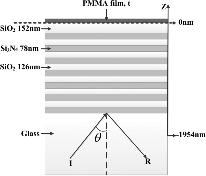
A schematic diagram of the sample used for this investigation is shown in Figure 1. The 1DPC is composed of repeated layers of SiO2 and Si3N4. The thicknesses of SiO2 and Si3N4 layers are 126 nm and 78 nm, respectively. The top layer of the 1DPC is made of low dielectric SiO2, with the thickness of 152 nm. This configuration was shown to display a Transverse Electric (TE) polarized BSW at the interface between the 1DPC and the air.17 PMMA films of different thickness (t) are spin-coated onto the 1DPC. The optical modes in the PMMA film coated 1DPC are investigated using transfer matrix method (TMM) where we calculated the angle dependent reflectivity from the 1DPC. The wavelength of the TE-polarized light is 600 nm. The incident angle is represented as θ, which ranges from 35° to 70°. The refractive indices of the air, PMMA, SiO2, Si3N4, and glass substrate are assumed to be 1.0, 1.49 + 10−5i, 1.46 + 10−5i, 2.14 + 3 × 10⁻⁴i, and 1.52, respectively.
Figure 1.
A schematic diagram of the 1DPC coated with PMMA film. The thicknesses of the repeated SiO2 and Si3N4 layers are 126 nm and 78 nm, respectively. The thickness of the top SiO2 layer is 152 nm. A various thickness of the PMMA film is used and represented with t. The incident angle is θ. The horizontal blue dashed line (at Z = 0 nm) represents the 1DPC-PMMA interface. I represents the incident light and R the reflected light.
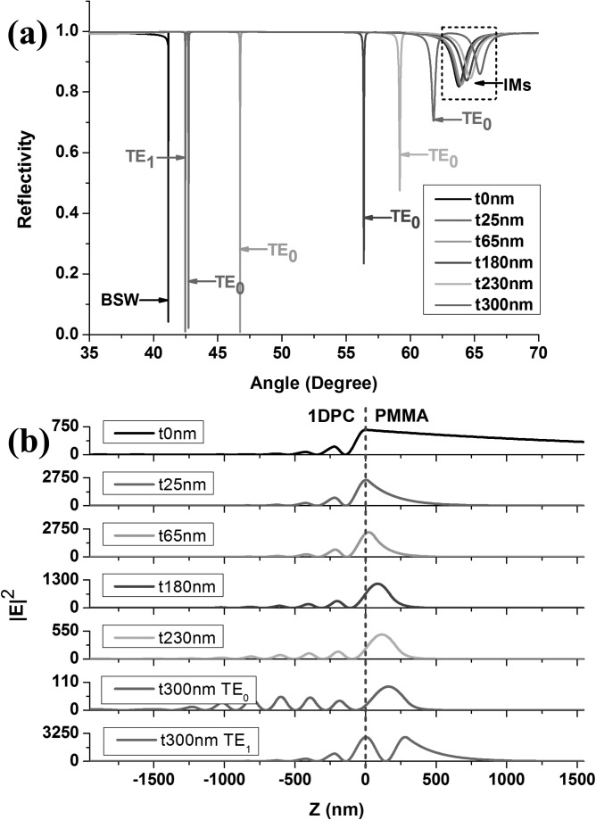
Figure 2a presents the corresponding angle dependent reflectivity curves for different thicknesses of the PMMA film (t = 0, 25, 65, 180, 230, and 300 nm). For each curve, two reflectivity dips are noticed. The broad dips at the large incident angles correspond to the internal modes (IMs) inside the 1DPC, where the electric-magnetic field is oscillating inside the 1DPC.18, 19 The sharp dips at the small incident angles represent the excitation of the optical surface modes of the 1DPC with lower propagation loss. The internal modes inside the 1DPC are insensitive to the PMMA film thickness. Whereas the resonant angle of the surface modes (sharp dips) is PMMA film thickness dependent. Accordingly, in this Letter, we primarily focused our attention on the properties of the surface optical modes of the 1DPC. The observed angles for the surface modes are 41.15°, 42.76°, 46.74°, 56.38°, and 59.18° for 0, 25, 65, 180, 230, and 300 nm thick PMMA layer on 1DPC, respectively. The larger resonant angles mean the larger effective index of these propagating modes. When the PMMA film thickness is further increased to 300 nm, three reflectivity dips are noticed, as shown in Figure 2a. The resonant angles of the first (TE1) and second (TE0) dips are 42.48° and 62.81°, respectively.
Figure 2.
(a) Calculated angle dependent reflectivity curves at 600 nm for the PMMA coated 1DPC shown in Figure 1. The thicknesses of the PMMA film are 0, 25, 65, 180, 230, and 300 nm, respectively. The incident light is S-polarized, 600 nm wavelength. (b) The electric field intensity |E|2 profiles on the line across the 1DPC along the Z-axis. The incident angles are fixed at the resonant angles shown in panel (a), which are 41.15°, 42.73°, 46.74°, 56.38°, 59.18°, 61.81°, and 42.48°. The vertical blue dashed line in panel (b)represents the interface between the 1DPC and the PMMA film.
To reveal the optical properties of these surface modes, electric-field intensity (|E|2) distribution along the Z-axis is plotted in Figure 2b. For each thickness of the PMMA films, the incident angle is fixed at the corresponding resonant angle of the sharp dip. The incident light is S-polarized or TE polarized. The blue dash line (at Z = 0 nm) in Figure 2b represents the interface between the 1DPC and the PMMA as illustrated in Figure 1a. When the thickness of the PMMA is 0 nm, the strongest electric field (E-field) is located at the 1DPC-Air interface. The E-field decays slowly with the increasing of the vertical distance from the 1DPC-Air interface. This field distribution is a typical feature for the BSW. So we assign this mode as the BSW and the sharp dip at 41.15° corresponds to the BSW resonance.
However, when the PMMA film is coated on the 1DPC, even its thickness is only 25 nm, we found that the position of the strongest |E|2-field shifts into the PMMA layer. For example, when t = 0, 25, 65, 180, 230, and 300 nm, the Z-positions of the maximum field intensity are Z = 0, 6, 23, 86, 116, and 163 nm, respectively. On the other hand, with the presence of the PMMA layer, the |E|2-field decays much quickly, which means that the optical field becomes more spatially confined to the 1DPC. Due to the difference in the |E|2-field distribution, the optical modes inside the PMMA films may not be seemed as the purely BSW. The modes are more like the TE0 guided modes especially when the PMMA layer becomes thick, such as t = 180 nm or 230 nm. When the thickness of PMMA is small, such as 25 nm or 65 nm, the propagating mode seems to be the hybrid state between BSW and TE0 guided modes. When the thickness of the PMMA film is further increased to 300 nm, two TE guided modes (two dips at 42.48° and 62.81°) appeared as shown in Figure 2a. Based on the field distributions shown in the last two panels of Figure 2b, the dip at 42.48° corresponds to TE1 guided mode and the dip at 61.81° to the TE0 guided mode.
It is well known that for ordinary asymmetrical dielectric planar waveguides, when the thickness of the guided layer is too small, there is no propagating mode inside the waveguide.20 In our work, the PMMA film coated 1DPC can be seen as an asymmetrical planar waveguide where the PMMA film works as the guided layer. The above simulations verify that for the asymmetrical planar waveguide made of 1DPC there is no cut-off thickness of the guided layer and the propagating modes can exist even the PMMA layer is very thin, such as 0 nm or 25 nm. For this kind of asymmetric planar waveguide, the propagating modes on the 1DPC evolve from BSW to guided modes with the increasing of the PMMA film thickness.
To verify the numerical simulations, we studied the fluorescence emission coupling patterns of 1DPC coated with Rhodamine B (RhB) doped PMMA film by using back focal plane imaging (BFP). This method reveals the angular distribution of light which exits through the glass substrate. The 1DPC with the structural parameters shown in Figure 1 is fabricated with the plasma-enhanced chemical vapor deposition (PECVD). Rhodamine B (RhB) doped PMMA films with thickness of 0, 25, 65, 180, 230, and 300 nm are spin-coated onto the 1DPC. Under the excitation of 532 nm laser, the RhB molecules can emit fluorescence at 600 nm. The optical energy couples into the optical modes on the PMMA coated 1DPC. At this time, it is not clear if the coupling occurs directly with the excited state fluorophores, or if the fluorophores first emit then subsequently couple with the propagating modes of the structure. But the experimental results verify that the excited molecules, such as dye molecules, can work as a point source to generate the corresponding optical modes inside the micro or nanostructures.21, 22 Leakage radiation microscopy (LRM) is used to detect the emitting angles of the optical modes-coupled fluorescence which correspond to the resonant dips (or angles) on the Figure 2a.23, 24, 25 A polarizer is placed before the CCD camera to determine the polarization state of the emitting fluorescence, which can also determine the polarization of the polymer loaded optical modes on the 1DPC. A band pass filter with center wavelength at 600 nm is used to allow only fluorescence at this wavelength to reach the CCD camera. The band width of the spectra filter is about 10 nm.
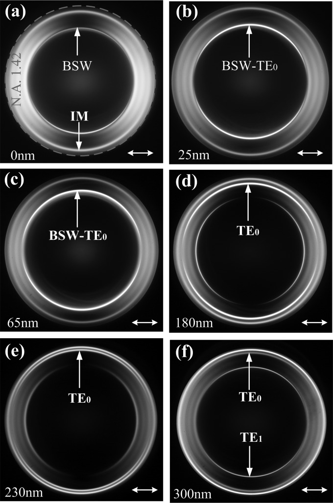
Figure 3 shows the BFP images of the fluorescence emission from the 1DPCs with different thickness of the RhB doped PMMA film (t = 0, 25, 65, 180, 230, and 300 nm). In the case of t = 0 nm, the 1DPC was immersed in the RhB alcohol solution for 30 min. Then, the 1DPC was taken and washed briefly with deionized (DI) water and nitrogen blowed dry. The BFP images show the coupled-emission as bright rings. It is known that these bright rings on the BFP images mean that the dye molecules are coupled with the optical modes and induced the directional fluorescence emission. From the diameter of the bright ring and the outer ring (labeled with the red-dashed line on Figure 3a, corresponding to the largest collection angle of the objective, 69°), the emitting angle of the fluorescence can be derived. Based on the above numerical simulations, we pay our attention to the small bright rings (labeled with the single-headed arrows), which are corresponding to the BSWs or TE guided modes or their hybrid states. The larger rings are corresponded to the IMs where the optical field oscillates inside the 1DPC multilayer. The fluorescence intensity distribution of the bright rings in the case of a linear polarizer demonstrates that the polarization direction of the fluorescence is along the azimuthally direction of the ring which corresponds to the S-polarization or TE polarization and is consistent with the numerical simulations (Figure 2).26, 27
Figure 3.
BFP images of the RhB fluorescence emission from the 1DPC coated with PMMA film. The thickness of the PMMA film is 0 (a), 25 (b), 65 (c), 180 (d), 230 (e), and 300 nm (f). The white double-headed arrow lines represent the direction of the polarizer. The red circular dashed line on (a) represents the numerical aperture (N.A.) of the collection objective (1.42).
For comparison, the emitting angles derived from the BFP images and the calculated resonant angles for different thicknesses of the PMMA films are listed in Table TABLE I.. The experimental results are in very close agreement with the calculations. We noticed consistent increase of the resonant angles with the increase of the polymer thickness. At t = 300 nm, both TE0 and TE1 modes are generated. Small discrepancy in the observed versus the calculated angles might be due to the mismatch of the actual PMMA thickness to that used in the calculations. However, it is interesting to note that the experimental results verify the existence of the BSW or TE guided modes or their hybrid modes in the polymer film coated on the 1DPCs. This study reveals the evolution from BSW to TE guided modes with the increasing thickness of the PMMA films.
TABLE I.
Experimental and calculated (600 nm wavelength) resonant angles of the BSWs or TE guided modes inside the polymer films on the 1DPC.
| 0 nm | 25 nm | 65 nm | 180 nm | 230 nm | 300 nm | 300 nm | |
|---|---|---|---|---|---|---|---|
| Experimental | 41.14° | 42.40° | 46.73° | 55.45° | 58.71° | 59.63° | 43.20° |
| Calculated | 41.15° | 42.73° | 46.74° | 56.38° | 59.18° | 61.81° | 42.48° |
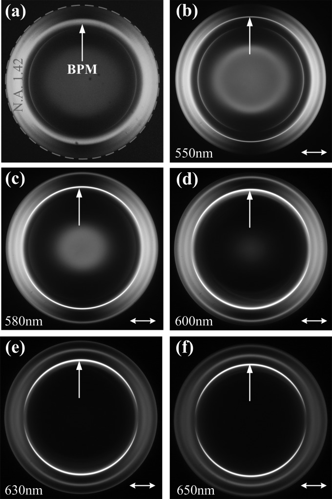
The broad emission spectrum of RhB molecules provides the opportunity to understand the evolution of surface optical modes in the PMMA film for different wavelengths. In this regard, a 532 nm long-pass filter and a range of band-pass filters with center wavelengths of 550 nm, 580 nm, 600 nm, 630 nm, and 650 nm are used to select the respective wavelengths. We chose 65 nm thick PMMA film on the 1DPC for this study. Figure 4a shows the BFP image with a 532 nm long-pass filter before the color CCD camera. We can see a color ring, labeled with broad band propagating mode (BPM), in the BFP image. The color of the ring gradually changes from red to green with the increasing the diameter. When the band-pass filters are used, we can find that the diameter of the bright rings (shown with single-headed arrows) in Figures 4b, 4c, 4d, 4e, 4f decreases with the longer wavelengths of the fluorescence. The polarization of the fluorescence on the bright rings has S-polarization or azimuthally polarization. Further, we calculated the resonant angles of the hybrid state of the BSWs and TE0 modes at these wavelengths and shown in Table TABLE II.. As we can see, the calculated values are consistent with the experimentally observed values, which further corroborates that the propagating TE polarized modes can be sustained in the polymer layer coated on 1DPCs.
Figure 4.
BFP images of the fluorescence emission from the 1DPC coated with PMMA film. The thickness of the PMMA film is 65 nm. Panel (a) is the BFP image captured by a color CCD camera with a 532 nm long-pass filter. Panels (b)-(f) are taken with the black and white camera combined with the band-pass filters. The selected wavelengths of the fluorescence are 550, (b), 580 (c), 600 (d), 630 (e), and 650 nm (f), respectively. The white double-headed arrows represent the direction of the polarizer. BPM is the abbreviation of broad band propagating mode. The red dashed-circular line on panel (a) represents the numerical aperture (N.A.) of the collection objective (which is 1.42).
TABLE II.
Experimental and calculated resonant angles of the BSW or TE guided modes at different wavelengths.
| 550 nm | 580 nm | 600 nm | 630 nm | 650 nm | |
|---|---|---|---|---|---|
| Experimental | 50.73° | 48.46° | 46.73° | 44.41° | 42.81° |
| Calculated | 50.02° | 48.06° | 46.74° | 44.76° | 43.45° |
In conclusions, our work provides a thorough investigation on the propagating modes within a dielectric PMMA film on the 1DPC. Both numerical and experimental results verify that existence of the propagating modes loaded by the polymer films on the 1DPC without a cut-off thickness. The propagating modes will evolve gradually from TE polarized BSWs to TE guided modes by increasing the thickness of the polymer films. The field distributions or behaviors of these two kinds of modes are different, such as mode volume and position of the E-field maximum. The determination of these two kinds of modes is of great importance in optical sensing, integrated optics, and some E-field enhancement effects (such as SERS). The all dielectric materials used in this type of asymmetrical planar waveguide will induce lower propagation loss than that of the polymer loaded SPP waveguide.28, 29
Acknowledgments
This work was supported by the National Key Basic Research Program of China under Grant Nos. 2012CB921900, 2012CB922003, and 2013CBA01703, the National Natural Science Foundation of China under Grant Nos. 11374286 and 61036005. This work was also supported by NIH Grant Nos. RO1HG002655, RO1EB006521, and RO1HG005090. We thank UMCP Fab Lab.
References
- Smolyaninov I. I., Hung Y.-J., and Davis C. C., Appl. Phys. Lett. 87, 241106 (2005). 10.1063/1.2142096 [DOI] [Google Scholar]
- Barnes W. L., Dereux A., and Ebbesen T. W., Nature 424, 824 (2003). 10.1038/nature01937 [DOI] [PubMed] [Google Scholar]
- Raether H., Surface Plasmons on Smooth and Rough Surfaces and Gratings (Springer, Berlin, 1988). [Google Scholar]
- Maier S. A., Plasmonics: Fundamentals and Applications (Springer, 2007). [Google Scholar]
- Grandidier J., Colas des Francs G., Massenot S., Bouhelier A., Markey L., Weeber J. C., Finot C., and Dereux A., Nano Lett. 9, 2935 (2009). 10.1021/nl901314u [DOI] [PubMed] [Google Scholar]
- Descrovi E., Sfez T., Quaglio M., Brunazzo D., Dominici L., Michelotti F., Herzig H. P., Martin O. J. F., and Giorgis F., Nano Lett. 10, 2087–2091 (2010). 10.1021/nl100481q [DOI] [PubMed] [Google Scholar]
- Sfez T., Descrovi E., Yu L. B., Brunazzo D., Quaglio M., Dominici L., Nakagawa W., Michelotti F., Giorgis F., Martin O. J. F., and Herzig H. P., J. Opt. Soc. Am. B 27, 1617 (2010). 10.1364/JOSAB.27.001617 [DOI] [Google Scholar]
- Yeh P., Yariv A., and Hong C. S., J. Opt. Soc. Am. 67, 423–438 (1977). 10.1364/JOSA.67.000423 [DOI] [Google Scholar]
- Joannopoulos J. D., Johnson S. G., Winn J. N., and Meade R. D., Photonic Crystals, Molding the Flow of Light, 2nd ed. (Princeton university press, 2008). [Google Scholar]
- Sinibaldi A., Danz N., Descrovi E., Munzert P., Schulz U., Sonntag F., Dominici L., and Michelotti F., Sens. Actuators, B 174, 292–298 (2012). 10.1016/j.snb.2012.07.015 [DOI] [Google Scholar]
- Rivolo P., Michelotti F., Frascella F., Digregorio G., Mandracci P., Dominici L., Giorgis F., and Descrovi E., Sens. Actuators, B 161, 1046 (2012). 10.1016/j.snb.2011.12.006 [DOI] [Google Scholar]
- Frascella F., Ricciardi S., Rivolo P., Moi V., Giorgis F., Descrovi E., Michelotti F., Munzert P., Danz N., Napione L., Alvaro M., and Bussolino F., Sensors 13(2 ), 2011–2022 (2013). 10.3390/s130202011 [DOI] [PMC free article] [PubMed] [Google Scholar]
- Farmer A., Friedli A. C., Wright S. M., and Robertson W. M., Sens. Actuators, B 173, 79–84 (2012). 10.1016/j.snb.2012.06.015 [DOI] [Google Scholar]
- Konopsky V. N. and Alieva E. V., Biosens. Bioelectron. 25, 1212–1216 (2010). 10.1016/j.bios.2009.09.011 [DOI] [PubMed] [Google Scholar]
- Toma K., Descrovi E., Toma M., Ballarini M., Mandracci P., Giorgis F., Mateescu A., Jonas U., Knoll W., and Dostálek J., Biosens. Bioelectron. 43, 108–114 (2013). 10.1016/j.bios.2012.12.001 [DOI] [PubMed] [Google Scholar]
- Guo Y., Ye J. Y., Divin C., Huang B., Thomas T. P., Baker J. R., and Norris T. B., Anal. Chem. 82, 5211–5218 (2010). 10.1021/ac100576y [DOI] [PMC free article] [PubMed] [Google Scholar]
- Badugu R., Kazimierz N., Descrovi E., and Lakowicz J. R., Anal. Biochem. 442, 83–96 (2013). 10.1016/j.ab.2013.07.021 [DOI] [PMC free article] [PubMed] [Google Scholar]
- Ballarini M., Frascella F., Michelotti F., Digregorio G., Rivolo P., Paeder V., Musi V., Giorgis F., and Descrovi E., Appl. Phys. Lett. 99, 043302 (2011). 10.1063/1.3616144 [DOI] [Google Scholar]
- Zhang D. G., Badugu R., Chen Y. K., Yu S. S., Yao P. J., Wang P., Ming H., and Lakowicz J. R., “ Back focal plane imaging of directional emission from dye molecules coupled to one-dimensional photonic crystals,” Nanotechnology (in press). [DOI] [PMC free article] [PubMed]
- Lifante G., Integrated Photonics: Fundamentals (Wiley, England, 2003). [Google Scholar]
- Zhang D. G., Yuan X.-C., Bouhelier A., Wang P., and Ming H., Opt. Lett. 35(3 ), 408–410 (2010). 10.1364/OL.35.000408 [DOI] [PubMed] [Google Scholar]
- Ballarini M., Frascella F., Enrico E., Mandracci P., De Leo N., Michelotti F., Giorgis F., and Descrovi E., Appl. Phys. Lett. 100, 063305 (2012). 10.1063/1.3684272 [DOI] [PubMed] [Google Scholar]
- Chen Y. K., Zhang D. G., Wang X. X., Liu C., Wang P., and Ming H., Nanotechnology 23, 475202 (2012). 10.1088/0957-4484/23/47/475202 [DOI] [PubMed] [Google Scholar]
- Regan C. J., Rodriguez R., Gourshetty S. C., Grave de Peralta L., and Bernussi A. A., Opt. Express 20(19 ), 20827–20834 (2012). 10.1364/OE.20.020827 [DOI] [PubMed] [Google Scholar]
- Zhang D. G., Yuan X. C., and Bouhelier A., Appl. Opt. 49(5 ), 875–879 (2010). 10.1364/AO.49.000875 [DOI] [PubMed] [Google Scholar]
- Zhan Q. W., Adv. Opt. Photonics 1, 1–57 (2009). 10.1364/AOP.1.000001 [DOI] [Google Scholar]
- Angelini A., Enrico E., De Leo N., Munzert P., Boarino L., Michelotti F., Giorgis F., and Descrovi E., New J. Phys. 15, 073002 (2013). 10.1088/1367-2630/15/7/073002 [DOI] [Google Scholar]
- Holmgaard T. and Bozhevolnyi S. I., Phys. Rev. B 75, 245405 (2007). 10.1103/PhysRevB.75.245405 [DOI] [Google Scholar]
- Steinberger B., Hohenau A., Ditlbacher H., Stepanov A. L., Drezet A., Aussenegg F. R., Leitner A., and Krenn J. R., Appl. Phys. Lett. 88, 094104 (2006). 10.1063/1.2180448 [DOI] [Google Scholar]


