Abstract
We provide the in-depth characterization of light-polymer nanowire interactions in the context of an effective Mie scattering regime associated with low refractive index materials. Properties of this regime sharply contrast with these of resonant Mie scattering, and involve the formation of strictly forward-scattered and coupling-free optical fields in the vicinity of core-shell polymer nanowires. Scattering from these optical fields is shown to be non-resonant in nature and independent from incident polarization. In order to demonstrate the potential utility of this scattering regime in one-dimensional (1D) polymeric nanostructures, we fabricate polycarbonate (PC) - polyvinylidene difluoride (PVDF) core-shell nanowires using a novel iterative thermal drawing process that yields uniform and indefinitely long core-shell nanostructures. These nanowires are successfully engineered for novel nanophotonics applications, including size-dependent structural coloration, efficient light capture on thin-film solar cells, optical nano-sensors with ultrahigh sensitivity and a mask-free photolithography method suitable for the straightforward production of 1D nanopatterns.
Light-matter interactions depend strongly on both intrinsic and extrinsic properties of the interacting materials and are responsible for a wide variety of nanoscale optical phenomena, some of which can be described under the Mie theory. Examples of optical interactions within the domain of Mie theory include light scattering from particles with high refractive indices1 and sizes smaller than the wavelength of the incident light, which occurs via the resonant form of Mie scattering. In addition, Mie theory also encompasses the confinement of light into deep-subwavelength structures via cluster oscillations of free electrons2,3, which is most pronounced in metallic nanostructures, and the observation of resonant absorption effects in high-index semiconductors4,5. All of the above optical mechanisms are associated with a number of unique applications in nanophotonics. However, the interaction of light with low refractive-index nanomaterials6,7, such as polymers and some glasses, has not been very well-investigated, and its characterization may reveal many unknown and potentially distinctive optical features.
Polymers are particularly attractive for nanomaterial fabrication efforts, as many polymer materials are cheap, flexible and easy to produce large scales. However, one-dimensional nanoscale polymer structures are not used as frequently as their macro-scale counterparts. Polymers lack many desirable optical and optoelectronic features displayed by metals and semiconductors, and this deficit is especially pronounced in photonics. Despite their disadvantages, however, polymer nanostructures have been utilized for several photonics applications so far, including in sensors8, organic light-emitting diodes (OLEDs)9, field-effect transistors (FETs) and lasing10. Such applications primarily rely on the intrinsic features of polymers, and little work has been performed on how the extrinsic properties of polymer nanostructures alter the optical effects associated with these materials.
In this study, we report that effective Mie scattering can occur in a specific region characteristic to polymer materials, and potentially other low-refractive index wavelength-scalable nanostructures. Decreases in the refractive index of a resonant dielectric nanostructure, when complemented with increasing nanostructure diameters, lead to the creation of a region where light is forced to scatter from the core region, as opposed to resonating within it. As such, within specific ranges of refractive indices and nanostructure diameters (i.e. within a specific region in the n-d domain of classical Mie scattering, where n and d are refractive index and structure diameter, respectively), the scattering of light is markedly different from high-index and deep-subwavelength scattering phenomena, and can be described as a non-resonant form of Mie scattering. This region has also been called an “anomalous diffraction” zone11, and so far remains poorly characterized.
Due to their low refractive indices and flexibility in material choice, polymer nanowires are exceptionally suitable for the characterization of this scattering regime, as well as for their use in practical applications. However, while powerful and versatile methods, such as ion etching12, laser irradiation13, template wetting process14,17, electrospinning15,16, solution chemistry18 and nanolithography19, are available for the fabrication of polymer nanostructures, a wide range of issues are nonetheless associated with current production efforts. For device applications, polymer nanostructures are required to be sufficiently long, well-ordered and uniform, which is difficult to achieve by conventional fabrication techniques. In this study, we successfully produce all-polymer PC-PVDF core-shell nanowires displaying non-resonant Mie scattering by exploiting a novel thermal drawing technique20. One-dimensional polymer nanostructures are obtained in well-controlled and consistent sizes and morphologies, and in aspect ratios reaching 1011, by using this top-down nanofabrication approach.
We perform a comprehensive investigation of the properties of this scattering regime, with emphasis on its potential utility in the design of polymer-based devices. The properties of non-resonant scattering are found to differ significantly from these of resonant Mie scattering, in being characterized by coupling-free and polarization-independent light scattering in the forward direction. We also demonstrate the applicability of this phenomenon in device design by experimentally and theoretically engineering these polymer nanostructures for the range of purposes. First, we observe diameter-dependent coloration on polymer nanowires, which serves as a conspicuous illustration of the structural coloration phenomenon using non-resonant Mie scattering. Secondly, we utilize the non-resonant Mie scattering effect as an effective means of light trapping, and perform theoretical predictions for nanowire sizes effective for use as light-capture materials in contemporary thin-film solar cells. Thirdly, we employ the relation between scattering characteristics and polymer material properties to engineer a novel refractive index sensor displaying size-dependent sensitivities exceeding 2000 nm/RIU for core radii of 400 nm. Finally, we use the forward-scattering and focusing behavior of non-resonant Mie scattering in the design of an effective mask-free photolithography method, called “Photonic Nanoblade Lithography”, which utilizes low-index arrays of aligned polymer nanowires to produce series of 1D nanopatterns.
Characterization of non-resonant Mie scattering regime
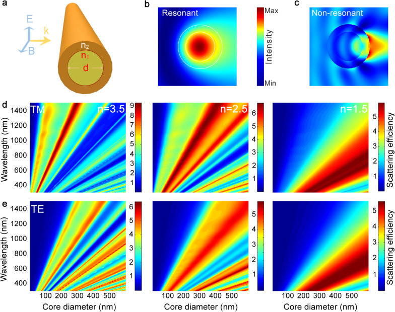
At scales below or on the order of the wavelength of the incident light, particle sizes may have significant effects on scattering behavior (Figure 1a). The interplay between the refractive index and the radial size of the scattered particle results in variable scattering properties, such as the occurrence of leaky mode resonant behavior in deep-subwavelength and high-refractive index materials (e.g. chalcogenide glasses1 and silicon21). Resonance occurs when the incident light is trapped inside the structure, and is exemplified by phenomena such as Fabry-Perot resonances, whispering gallery modes, or resonant Mie scattering (Figure 1b, Video S1). Interaction of light with polymeric nanostructures, however, displays non-resonant behavior, which can also be inferred from near field profiles of scattered light from a low-index core-shell nanowire geometry (Figure 1c, Video S2). In this type of scattering, light is scattered at specific ranges of wavelengths depending on the diameter of 1D nanostructures and falls under the purview of Mie theory. As such, we refer to this scattering behavior as non-resonant Mie (NRM) scattering.
Figure 1. Mie scattering from nanostructures.
(a) Schematic illustration of light scattering from core-shell nanostructures. Near-field profiles for scattered fields of (b) resonant and (c) non-resonant regimes. In the resonant regime, light is confined within the nanowire and scatters under leaky mode behavior. However, for low-refractive indices, light cannot be trapped inside nanowires and is instead scattered immediately in the forward direction, passing directly through the structure. (d–e) Using finite difference time domain (FDTD) method, a gradual transition from resonant to non-resonant Mie scattering regimes can be observed by reducing the refractive index of the nanostructure core. While changes between the modes of TE and TM polarizations are observed in higher refractive indices, scattering maps are nearly identical for the low refractive index medium for both polarization types.
Size-dependence and the broad scattering peaks of this regime are reminiscent of thin-film interference in low-index substrates, which relies on multiple reflections or refractions from the boundaries of different media. NRM scattering can be considered to be analogous to this effect: Both phenomena are thickness-dependent, and the low quality factor (Q, which describes the degree of resonance within the optical cavity) of thin-film interference in low-refractive index materials is similar to that of NRM scattering, and is caused by the inability of light to oscillate within the structure. While conventional high-Q resonators typically possess quality factors of up to 1010, this factor is exceedingly low (c. 10° or lower) in the present scattering regime. This shows that low-refractive index structures do not act as resonant cavities, and instead can intensify the transmitted light towards the propagating direction. The transition from resonant to non-resonant regimes of Mie scattering can be observed by reducing the refractive index of the nanostructure (Figure 1d, e). While splitting is observed between the TE and TM polarization modes in higher refractive indices, scattering maps are nearly identical in low refractive index media for both polarization types.
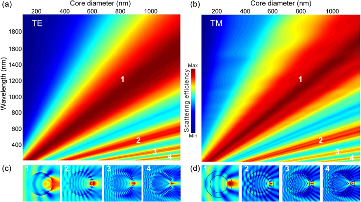
Detailed analysis of NRM scattering can be performed by characterizing the behavior of higher orders together with their field distribution profiles. Higher orders of TE and TM polarizations are found to appear in extended diameter and wavelength ranges (Figure 2a, b). They are also observed to exhibit a focusing effect and non-resonant field profiles for both polarizations (Figure 2c, d). Unlike the first order, peaks associated with the higher orders are relatively narrow. In Mie scattering, particle sizes are comparable to the wavelength of the incident light, while geometric optics is sufficient to explain the light-particle interactions for diameter to wavelength ratios over 10. For example, the fourth scattering order in our calculations appears in the ~200 nm wavelength region for a structure with a core diameter of ~1200 nm, which means that the structure is ~6 times larger than the wavelength of light (Figure 2a, b). As such, very higher orders of scattering can be approximated using geometrical optics. In addition to NRM scattering, polymer wires produced in higher diameters (i.e. in the microscale) are expected to display behaviors similar to these shown by many spherical and toroidal microresonators, which utilize phase matching conditions in order to create high-order whispering gallery modes. Lower orders of whispering gallery modes22 do occur in our polymer nanowires, but their contribution is not significant, as their excitation also requires phase matching conditions (e.g. tapered fiber coupling).
Figure 2. Detailed map of NRM Scattering.
NRM scattering maps of core-shell polymer nanowires for (a) TE and (b) TM polarizations. Extending the wavelength and diameter ranges for the case n = 1.5 (see Figure 1) results in the appearance of higher orders. Electric field profiles of corresponding orders of (c) TE and (d) TM polarizations exhibit strong directional scattering. Field profiles confirm the non-resonant nature of the NRM scattering regime.
NRM scattering is applicable for diverse set of nanostructural architectures, though a cylindrical core-shell geometry is chosen for the aforementioned calculations to simplify the eventual fabrication of the simulated structures. Theoretical calculations also account for the presence of a PVDF shell layer (the refractive index of which is assumed to be constant at 1.41 over the 300–1500 nm range), which is found not to significantly alter the optical properties of core-shell polymer nanowires1, but does have a minor effect on the effective size of our nanowires, especially for NRM scattering. As such, bare nanowires yield similar results to their core-shell equivalents (Figure S1a). Theoretical calculations are also provided for nanotubes, the hollow nature of which can be utilized in microfluidics-based sensing applications. Compared to nanowires, NRM scattering in nanotubes is associated with narrower scattering peaks, and their electric field profiles, while non-resonant, are somewhat diffuse (Figure S1b). We also investigate the scattering features of low-index subwavelength spheres, which are found to be similar to these of nanowires (Figure S1c). It is particularly notable that scattering from these nanospheres are fully independent from polarization, lacking the minor polarization-dependent shifts observed in nanowires (see Figure 3c).
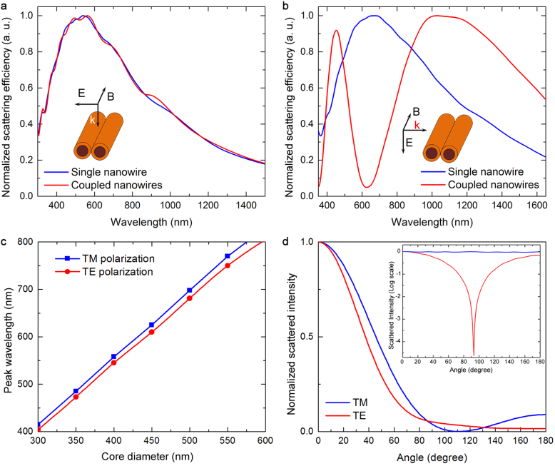
Figure 3. Optical properties of NRM scattering.
(a) Coupling-free scattering can be obtained for illumination perpendicular to the coupling axis of cylinders with 400 nm core diameter (as shown in the inset). (b) Mode splitting is observed when light is incident on coupled nanowires with identical core sizes. Detailed mode profiles for corresponding scattering peaks are provided in Figure S3c, d. (c) Scattering from low refractive index nanostructures displays a polarization independent behavior. (d) Far-field intensity profiles indicate that light is mostly scattered along the forward direction (e.g. for structure with 400 nm core diameter). Very high forward to backward scattering ratios are obtained for both polarizations. Inset: Far-field plots of resonant Mie scattering. Forward and backward scattering intensities are approximately in the same order. Structures are illuminated with a light source of 675 nm peak wavelength.
Characteristic features of NRM scattering regime
This scattering regime has several unique optical features. First of all, NRM scattering exhibits coupling-free behavior. Side-by-side nanostructures do not affect the characteristics of the scattered light (Figure 3a, Figure S2). Their intensity field profiles remain non-resonant and the focusing behavior is unchanged in the scattered field (Figure S3b). Light does not display oscillating behavior when it interacts with the polymer nanostructure, and the interaction in question occurs in durations short enough to preclude the excitation of even low order whispering gallery modes, which can contribute to sideways scattering behavior. As such, scattering only occurs on the propagating direction, and nanostructures can remain in close proximity without altering their scattering properties, as long as the structures are side-by-side and not overlapped (see below for details). In contrast, scattered light is significantly altered by the adjacency of particles in resonant Mie scattering, and this is undesirable in many practical cases. Consequently, it is suggested that the present mechanism is appropriate for large-scale applications.
Coupled-cavity resonance23 is an interesting optical phenomenon that is generally observed in resonant systems, and an analogous effect is also present in our polymer nanowires. In coupled (i.e. overlapped; see Figure 3a,b for schematics of side-by-side and overlapped structures) polymer nanowires, the main scattering peak at 650 nm is found to split into two peaks at 450 nm and 1060 nm (Figure 3b). The scattering preserves its non-resonant nature for the low energy peak at 1060 nm (see the field profile in Figure S3c). The higher energy peak at 450 nm displays coupling behavior, where the electric field is concentrated between two nanowires (see the field profile in Figure S3d). Unlike the resonant Mie effect (Figure 1d,e), NRM scattering in our polymer nanowires is also found to be polarization-independent (Figure 3c), which is critical for various applications, such as photovoltaics. There is a negligible shift between the scattering peaks of TE and TM polarizations; however, light scattering becomes a linear function of diameter and this shift disappears for unpolarized scattering. This observation also holds for higher orders of NRM scattering. Another important property of this domain is the strong forward scattering behavior observed in both polarizations (Figure 3d). Forward to backward scattering intensity ratio can exceed 50, which is markedly different from resonant Mie scattering, for which this ratio is around 1. As the scattering of light is mainly in the forward direction, this feature can be utilized in applications where the trapping of light is required. It is worth noting that there is almost no scattering in the sidelong direction for both polarizations. This explains why nanowires are coupling-free when arranged side-by-side, but strongly affected when overlapped.
Emerging applications of polymer nanowires
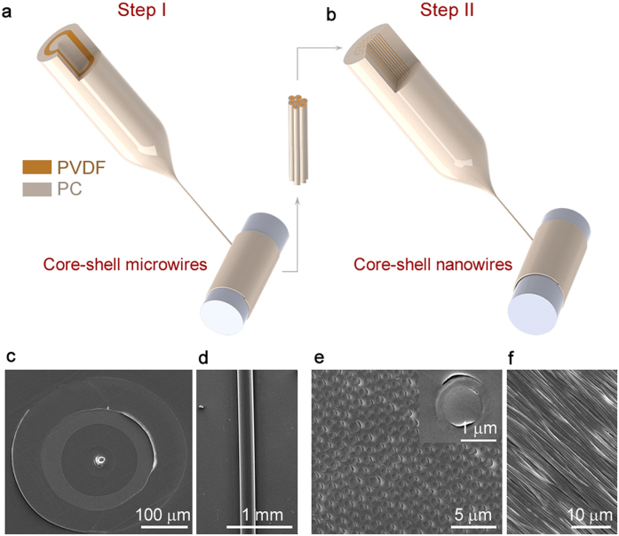
We had recently proposed and demonstrated a new top-down nanofabrication technique based on the iterative repetition of thermal drawing-based size reduction steps20, which we previously utilized in the production of chalcogenide based nanowires and piezoelectric nanotubes. Here, we use this fabrication method for reducing the size of cylindrical polymer core-shell structures from macro to nano dimensions (Figure 4a,b). Two polymers (PC and PVDF) are chosen as core and shell materials, and possess thermally and optically compatible properties that allow their design in a pattern that optimally facilitates the creation of non-resonant Mie scattering (i.e. a high-refractive index core and a low-refractive index shell region). Both of these materials are largely transparent in optical frequencies, and possess minimally varying refractive index values in the visible and NIR spectra (see Figure S4 for details on the optical properties of the relevant polymer materials). We obtain well-ordered and well-aligned in-fiber nanostructures as a result of fabrication process (see Methods for details). This step-by-step drawing technique allows the production of indefinitely long nanostructures, with exceptional aspect ratios of up to 1011. Cross-sectional and longitudinal SEM images of the structures obtained after first and second fabrication steps are shown in Figure 4c–f. All-polymer nanowires possess a radial core-shell aspect ratio of 2/3, which are similar to their macroscale counterparts. This ratio is assumed to be constant overall size ranges, and used in all our theoretical calculations.
Figure 4. Production of polymer nanostructures.
Iterative size reduction technique is used for production of all-polymer PC/PVDF core-shell nanowires. (a–b) Composite fibers obtained after the first thermal drawing step are cut and typically arranged in hexagonal lattices of several hundred fibers prior to a second drawing step. (c–e) Cross-sectional and (d–f) longitudinal SEM images of Step I and Step II structures. Step I core-shell microstructures possess an outer diameter of c. 240 μm. Kilometer-long, well-ordered, uniform and well-aligned polymer core-shell nanowire arrays can be obtained after the second drawing step.
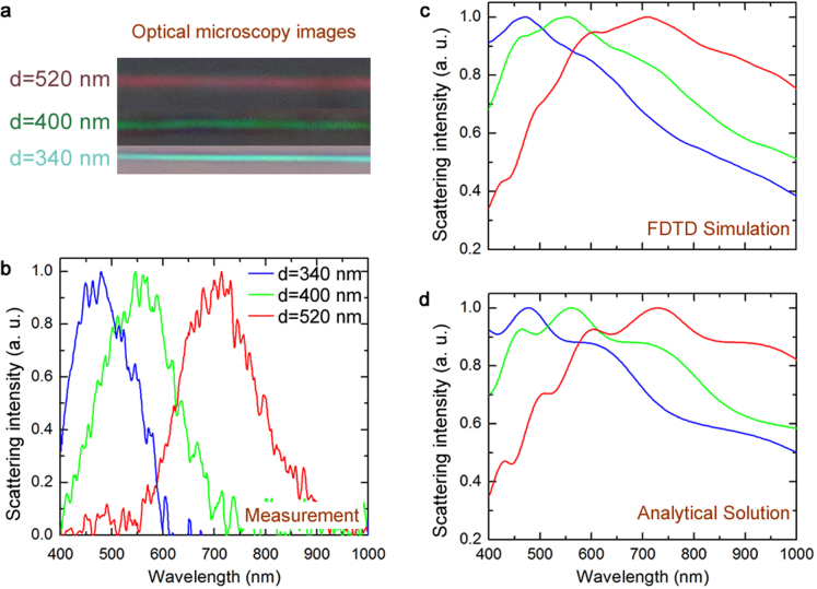
Fabricated low-index polymer nanowires are demonstrated to be effective in various novel applications utilizing the above-described properties of the NRM scattering regime. Unlike the first step output, step II nanowires are observed to display diameter-dependent structural coloration as a result of present effect. Free-standing structurally colored nanowires are obtained by etching the supporting layer with dichloromethane (DCM). Since the shell layer is resistant to DCM, the nanowires are unaffected by this etchant, provided that etching durations are kept sufficiently short. Nanostructures displaying blue, green and red coloration have been selected for analysis under inverted light microscope, and found to possess core diameters around 340 nm, 400 nm and 520 nm, respectively (Figure 5a–b; also see Figure S5 for the experimental setup of scattering measurements). Scattered light is collected by using a MAYA spectrometer. Optical images of colored nanostructures are taken by a digital camera attached to the microscope. Numerical results of scattering from core-shell nanostructure for TE and TM polarizations are simulated using an efficient and powerful simulation technique of FDTD method (see Methods for details), averaged to yield an approximation of unpolarized light, and compared with the scattering data from our experimental findings. Some discrepancy exists between our measurement and simulation results, especially with regards to our FWHM values. This is most probably attributable to our use of the reflection mode in our inverted microscopy experiments. While Mie scattering is mainly in the forward direction, there is also a finite amount of reflected intensity, and we use the latter in order to determine our experimental results. We have attempted to eliminate the contribution of specular reflection by subtracting the background specular reflection from our results; however, the remaining diffuse scattering spectrum admittedly suffers from noise. As such, our experimental results agree with our theoretical predictions in hue, but not in FWHM. Our experimental setup does not permit the direct measurement of forward-scattered light, but more precise results should be obtainable with the use of the dark field mode of transmission. Scattering of light from 1-D nanostructures can also be expressed analytically. To verify the analytical results derived for TE and TM polarizations, we compare these results with FDTD simulations (Figure S7). Results are plotted for three different nanostructure sizes corresponding to red, green and blue coloration, and found to be in good agreement (Figure 5c, d). Details of analytical solutions are described in Methods and Supporting Information.
Figure 5. Structural coloration of polymeric nanostructures.
Light scattering from core-shell nanostructures designed for red, green and blue coloration is investigated experimentally and theoretically. (a) Optical microscope images of colored nanostructures. Blue, green and red hues are observed on nanowires with core diameters of 340, 400, and 520 nm, respectively. (b) Scattering measurements are performed by using inverted optical microscope in bright field mode (Detailed measurement setup is given in Figure S5). (c) Scattering from low refractive index nanostructures are simulated by using a FDTD technique with ellipsometric constants. (d) An analytical solution based on the vector wave harmonic expansion of scattered light is developed for core-shell geometry. Experimental measurements bear similar results with the analytical and simulated results in terms of peak wavelengths, though their full width half maximum (FWHM) values differ due to the low scattering intensity present during measurement (Detailed comparisons for analytical and FDTD calculations are provided in Figure S7).
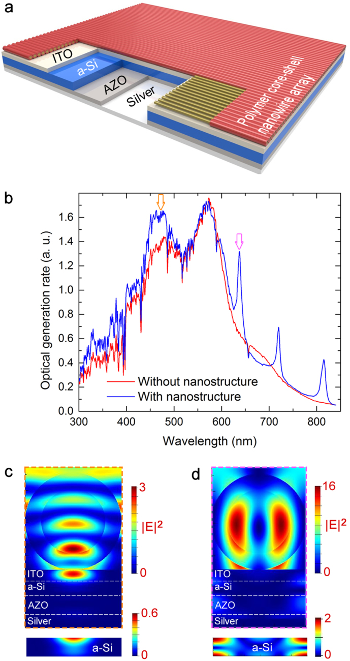
Low-refractive index materials are generally transparent in the visible spectrum, and are therefore desirable for many nanophotonics applications. Such materials are widely used for the enhancement of light absorption in solar cells, and can be applied as nanostructured coatings on optoelectronic devices and antireflective systems24,25. Recently, it was shown that subwavelength spheres composed of silica material boost light absorption efficiency26 via nanosphere to thin-film amorphous silicon coupling. As these spheres are composed of a low refractive index material and meet the size conditions required for NRM scattering, our work suggests that NRM scattering contributes significantly to this enhancement. In addition, the polarization independency, forward scattering behavior and unique coupling properties of this phenomenon are promising for the design of novel absorption enhancers. We therefore investigate the potential of NRM scattering for absorption enhancement by simulating the behavior of PVDF-PC polymer nanowires placed directly on a thin-film photovoltaic system (Figure 6a). The thin film solar cell utilized for theoretical investigations is composed of a silver back contact, an aluminum doped zinc oxide (AZO) layer, amorphous silicon absorbent and an indium tin oxide (ITO) front contact. Simulations are performed with and without a monolayer of core-shell nanowires on this solar cell design. The presence of polymer nanowires is associated with both peaked and broadband enhancements in the solar cell absorptivity, which are attributable to NRM scattering (Figure 6b).
Figure 6. Absorption enhancement by all-polymer core-shell nanowires.
(a) Core-shell nanowire arrays are simulated on top of a conventional thin film solar cell composed of a silver back contact, an AZO layer, an amorphous silicon absorbent and an ITO front contact. (b) Directional and coupling-free NRM scattering enhances the light absorption in the amorphous silicon layer, which results in an enhancement factor of 14%. The enhancement at 300–500 nm is polarization-independent and attributable to forward scattering feature of NRM scattering (c), while enhancements in the 500–800 nm region are caused by the strong coupling between the absorber and enhancer regions (d), characterized by shifts between the absorption peaks associated with TE and TM polarizations in this range (cf. Fig. S8 for details). TE polarization is used for the investigation of absorption enhancement, TM polarization yields similar results.
The enhancement at the 300–500 nm region is caused by forward and focused scattering characteristics of NRM scattering, which serve to intensify light absorption within the a-Si layer (Figure 6c). As NRM scattering displays polarization independency, enhancement at this region is identical for both TE and TM polarizations (Figure S8). In contrast, enhancement in the 500–800 nm region is created by a strong coupling interaction between the enhancer and absorber layers, analogous to behaviour existed for two coupled nanowire case (see Figure 3b, Figure S3c,d). It should be noted that the high-refractive index silicon layer exhibits resonant characteristics by itself, while our low-refractive index core-shell nanowires do not. When brought in close proximity, however, these two layers exhibit a distinct near field profile within both the a-Si thin film and the core-shell nanowire, which reminiscent of whispering gallery type modes (Figure 6d). This coupling behavior is dependent on type of polarization (i.e. TE or TM), resulting in shifts in the absorption peaks of TE and TM polarizations in the 500–800 nm region. The core-shell geometry displayed by our PC-PVDF nanowires is advantageous27 for absorption enhancement, as it stimulates more coupling modes than the bare nanowire geometry, and the shell region may allow efficient coupling by acting as a natural separator between core regions.
These enhancement domains can be altered by increasing or decreasing the diameter of the core-shell nanowires responsible for the enhancement, and overall absorption capacity can be optimized by moving these peaks onto regions where the absorptive layer displays poor absorptive capacity and solar radiation has it maximum contribution. Enhancement profiles of TE and TM polarizations show slight differences in their absorption peaks (especially in right side of absorption spectrum), though they induce similar enhancement rates (Figure S8). An overall enhancement of ~14% can be achieved for unpolarized light in amorphous silicon cells. This value reaches up to 20% when crystalline silicon is used as the absorbent material, and local enhancements are observed to exceed 300% in both cases. Simulations in Figure 6b are performed for TE polarization and the optical generation rate was calculated by integrating the product of solar spectrum intensities and the absorption within the silicon layer. Core diameter (PC) and shell thickness (PVDF) are set to 400 nm and 100 nm, respectively. Periodic boundary conditions are utilized in FDTD simulations in order to simplify theoretical calculations.
Optical nanosensors are another area that can benefit greatly from materials displaying NRM scattering-based effects. Dielectric materials find widespread use in resonator-based sensor systems28 as microspheres, photonic crystals, microcapillaries and diffraction gratings. A tradeoff between detection limit and sensitivity is generally observed in these systems. Both parameters can be significant in specific applications; for example, detection limit is crucial for molecular level sensing, while sensitivity can become an important factor in color sensors.
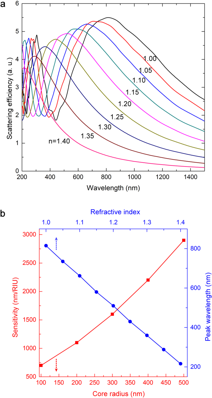
Sensitivity values of NRM scattering results are highly promising for refractive index-based sensor applications. As such, the use of NRM scattering may increase the sensitivity of low-index nanostructure-based measurement efforts, though at the expense of a low detection limit. In resonant Mie scattering, changes in the refractive index of the surrounding medium do not induce significant spectral shifts. However, when our PVDF-PC nanowires are placed in different solvent environments and the optical index of this ambient medium is increased from 1 to 1.4 with increments of 0.05, the broad peak of NRM-scattered light blueshifts and narrows in a refractive index-dependent manner for these core-shell polymer nanostructures (Figure 7a). Sensitivity values over 2000 nm/RIU are observed for core radii of 400 nm. For these sizes, NRM scattering peaks appear in the near infrared region, though embedding the polymer nanostructures in any common solvent will be adequate to pull the NRM peaks into the visible region (Figure 7b). To the best of our knowledge, our NRM scattering-based detection method reaches record values in sensitivity among any refractive index sensor, and is superior to cutting-edge plasmonics sensors in the visible spectrum29,30.
Figure 7. Sensitivity of NRM scattering based sensors.
(a) Rapid shifts in scattering spectra can be observed by changing the refractive index of the medium surrounding core-shell polymer structures with fixed core radii of 300 nm, and correspond to high sensitivity values. (b) Size-dependent sensitivity values (left and bottom axes) plotted with medium-dependent shifts of the peak wavelength (right and top axes).
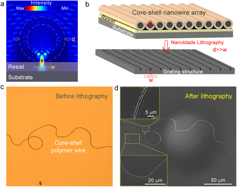
Low refractive index nanostructures strongly scatter light in the forward direction, and nanojets of low-index nanospheres are currently utilized in photolithography31 and super-resolution imaging32 efforts. However, the precise mechanism behind the scattering phenomenon is not fully described, which complicates the optimization of these processes. This type of scattering behavior is easy to predict and model in the context of NRM scattering, which enables the determination of lithography parameters for optimal fabrication performance. We therefore demonstrate the effectiveness of our NRM scattering-based models by employing our polymer nanowires in a lithographic fabrication method, which we call photonic nano-blade lithography (PNL) and believe to represent the first demonstration of a mask-free lithographic method capable of directly imprinting 1D nanopatterns. It is apparent from Figure 8a that scattered light focuses on area that is smaller than its physical dimensions. Any order of this scattering, therefore, can be used to concentrate scattered light in very small sizes, allowing the fabrication of high resolution structures. Using the first four orders of TM polarization, it is possible to focus incident light in spot sizes 3-fold, 9-fold, 15-fold and 20-fold smaller than that of the nanowire diameter, respectively. TE orders also possess similar focusing features (e.g. 1.5-fold, 4.5-fold, 9-fold and 18-fold reductions observed for first four orders of TE polarization). As side-by-side coupling does not occur in NRM, coupling effects will not interfere with the resulting pattern, as long as a single layer of nanostructures are employed (Figure 8b). An ultraviolet laser with a wavelength that corresponds to a specific scattering order can therefore be utilized to fabricate structures without the use of photomasks. We employ this capability to produce 1D nano-grating or nano-holes using arrays of low-refractive index, all-polymer core-shell nanowires. To this end, a single core-shell polymer wire is used to focus scattered light on a photoresist-covered surface, facilitating the localized absorption of the UV light throughout the photoresist (Figure 8c, see Methods). The exposed portion of photoresist, which corresponds to the region immediately below the nadir of the polymer wire, would then solidify or dissolve, depending on photoresist used. The surface pattern can then be utilized to obtain a series of 1D nanogratings. The present photolithography method is exceptional in that it allows the patterning of surfaces in arbitrary configurations, which is difficult to replicate using photomasks or sphere-based maskless lithography methods (see e.g. the wavy 1D nanoholes in Figure 8d, which are exactly imprints of the original polymer wire).
Figure 8. Photonic Nanoblade Lithography (PNL).
(a) Nano-blade lithography uses the focusing feature of NRM scattering in order to expose the photoresist in near subwavelength sizes. (b) Consequently, array of 1D grating structures or holes can be fabricated. (c) Single polymer wire used for the proof-of-concept demonstration of PNL technique. Polymer wire is laid on pre-coated photoresist. (d) After exposing sample into UV radiation and developing final structure, scheme of 1D nanohole imprinted original path is created. Thickness of polymer wire is 3.2 μm. The generated 1D hole possesses 400 nm widths.
Discussion and conclusion
The present manuscript details the characterization of a curious scattering regime associated with low-refractive index materials, describes the phenomenon displayed as a non-resonant form of Mie scattering, and utilizes a polymer nanowire design to illustrate the potential applications of this scattering domain. In stark contrast with resonant Mie scattering, non-resonant light scattering displays characteristic coupling features, polarization independency, and strictly forward-directed scattering and focusing behaviour.
Polymer structures similar to these described in the present manuscript can also be utilized in the design of fiber optic waveguides; however, it must be noted that the non-resonant Mie scattering phenomenon is distinct from waveguide behavior. In dielectric fiber waveguides, the basic confinement mechanism is total internal reflection, which permits the propagation of light within the longitudinal direction. As such, fiber waveguide modes can propagate whilst displaying multimode behaviour and are subject to cut-off wavelengths, beyond which no efficient transmission of mode is possible. This trait is fundamentally different from these exhibited by NRM scattering, which is characterized by discrete scattering orders. These differences are also apparently clear in the spectral behaviors33 and mode profiles34 of fiber optics and scattering effects, which suggests that these two phenomena can take place in similar sizes and geometries, but are reliant on different concepts.
Pure polymeric materials are relatively unpopular for optical applications, due to their difficulty of fabrication and the relative dearth of information on their optical properties. However, we find that all-polymer core-shell nanowires are capable of displaying effective non-resonant Mie scattering behavior, which allows their use in various applications; including nanosensors, photovoltaics, photolithography and structural coloration. The ease of fabrication afforded by our iterative size reduction method allows the convenient production of large arrays of all-polymer nanowires, as this thermal drawing method is a rapid process and comes at a reasonable cost. 1D polymer nanowires fabricated by ISR are self-aligned, uniform across large distances and can be produced for use in-fiber applications. Further, their all-polymer composition renders them ideal for flexible surface applications.
High-density arrays of polymer nanowires35 can also be obtained by the inclusion of a post-processing step within the fabrication scheme, and are optically interesting systems. The PC “sheath” containing step II or III fibers can be etched and the bare nanowires can be reassembled to create high-density core-shell polymer nanowire arrays. While one-dimensional structures composed of metals, semiconductors, and certain polymer materials have been described as potential environmental and health hazards, the use of PVDF and PC have been approved by the Food and Drug Administration (FDA). As such, the use of all-polymer PVDF-PC core-shell nanowires can be considered environmentally friendly and compatible with biological applications. By employing the iterative size reduction technique in the fabrication of polymer nanostructures with broad material options, we hope to assist in the emergence of many novel NRM-based applications based on all-polymer nanostructures, thus enhancing the toolbox of polymer materials at the nanoscale.
Methods
Macroscopic composite preparation, consolidation and thermal size reduction
We use commercially available PC and PVDF polymers as a core and shell layer, respectively. Their average refractive indexes are 1.41 for PVDF and 1.58 for PC (Figure S4), measured with a UV-Vis ellipsometer. Thermal compatibility of used polymers strengthens the performance of the thermal drawing process. First step preform preparation is started with wrapping 6 mm thickness of PC film, which acts as a core region, onto a glass tube with 4 mm outer diameter. Then, PVDF polymer with 4 mm thickness is rolled on PC layers. As a supporting layer, we again used PC and reached an overall diameter of 35 mm. The wrapped 20 cm long structure is thermally consolidated under vacuum (10−3 Torr), above the glass transition temperature of the both polymer to fuse (186°C for 55 minutes). Then resultant preform is thermally drawn in a custom-built fiber tower. By controlling critical drawing parameters, such as temperature, drawing speed, down feed speed, hundreds-meter long microstructures with 160 μm core diameters are obtained. About 500 of these microfibers are cut in 20 cm length and inserted into hollow core PC preform, for the second step fabrication. By repeating the same fabrication procedures we reached a core diameter of core-shell nanowires up to 200 nm. Likewise, process could be repeated for subsequent steps to reach sub-nanometer structures if required. In each drawing step, reduction factor can be arranged between 25 to 500 fold. In our case, the overall reduction factor at the end of two subsequent steps is 105. The nanowire diameter is controlled using a laser micrometer by monitoring the fiber diameter.
Analytical solutions
Lorenz-Mie formalism is used to solve problem of scattering from core-shell geometry. Firstly, incident plane wave, scattered field and the field inside the core and shell were expanded into vector cylindrical harmonics. Then, boundary conditions related to continuity of electric and magnetic field were applied at the core-shell and shell-air interface. Finally, coefficient of scattered field is extracted and scattering efficiency is found. Detailed information about solution procedures can be found in supporting information. Results of solved equations are given as in the following;
 |
where  ;
; 
 ;
; 
 |
where  ;
; 
 ;
;  .
.
Here m1 and m2 represent refractive indices of the core and the shell relative to the medium respectively. x = 2πa/λ, where a is radius of the core and y = 2πb/λ, where b is overall radius of the structure. Scattering efficiency for unpolarized light case can be expressed as;
 |
FDTD simulations
FDTD simulations are performed by using commercial finite-difference time-domain software (Lumerical Solutions Inc.) In most FDTD simulations, we illuminate our structure with Total Field Scattered Field (TFSF) source in 300–1500 nm wavelength range (particularly in solar cell application, incident source type is chosen as a planewave in 300–840 nm wavelength range). Scattering characteristics of particles can be studied with this source type, as the scattered field separated from the incident field, therefore permits for an efficient scattering analysis. FDTD simulations are calculated in two dimensional simulation regions by assuming cylindrical structures as indefinitely long. Frequency-domain power monitors are used to collect scattered light. Ellipsometric constants are inserted into simulations in Figure 5c. In theoretical investigation parts, refractive indices of polymers were taken as a constant.
Photolithography
A wafer with 500 μm thickness of silicon and 1 μm of thermal oxide layer is taken and diced into 20 mm × 20 mm pieces. One of the pieces is taken and first immersed in acetone. After 10 minutes of acetone-cleaning, the substrate is taken out and immersed in IPA (2-propanol) for 1 minute, and then in DI-water for 1 minute. The wafer is then rinsed with DI-water, blow-dried with nitrogen gas, and dried with hot plate at 120°C for 1 minute. The cleaned substrate is placed in a spinner. First, HMDS was spin-coated on the silica, and then the photoresist AZ5214E is spin-coated onto the HMDS (Spin speed: 4000 RPM, acceleration: 2000, 45 seconds). HMDS is used in order to increase the adhesion of the photoresist to the surface of the substrate. After spin-coating, the substrate is baked in a hot plate for 50 seconds at 110°C. After baking the photoresist, a piece of drawn and etched polymer wire is placed onto the substrate and is then patterned by lithography without using any photomask. The exposure dose of the UV light is 1 mJ/cm2. Following to exposure, fiber is removed from the surface of the substrate and photoresist is developed with 1:4 AZ400K developer.
Author Contributions
T.K. and M.B. designed and carried out research, analyzed data and wrote the paper. E.H. performed lithographic processes.
Supplementary Material
Video S1
Video S2
Supplementary
Acknowledgments
We would like to thank Alper D. Ozkan for critical reading of the manuscript and fruitful discussions. This work is supported by TUBITAK under the Project Nos. 110M412 and 111T696. The research leading to these results has received funding from the European Research Council under the European Union's Seventh Framework Programme (FP/2007–2013)/ERC Grant Agreement n. 307357. M.B. acknowledges partial support from the Turkish Academy of Sciences (TUBA).
References
- Khudiyev T., Ozgur E., Yaman M. & Bayindir M. Structural coloring in large-scale core-shell nanowires. Nano Lett. 11, 4661–4665 (2011). [DOI] [PubMed] [Google Scholar]
- Osberg K. D. et al. Dispersible gold nanorod dimers with sub-5 nm gaps as local amplifiers for surface-enhanced raman scattering. Nano Lett. 12, 3828–3832 (2012). [DOI] [PubMed] [Google Scholar]
- Kim S. et al. High-harmonic generation by resonant plasmon field enhancement. Nature 453, 757–760 (2008). [DOI] [PubMed] [Google Scholar]
- Cao L. et al. Semiconductor nanowire optical antenna solar absorbers. Nano Lett. 10, 439–445 (2010). [DOI] [PubMed] [Google Scholar]
- Kempa T. J. et al. Coaxial multishell nanowires with high-quality electronic interfaces and tunable optical cavities for ultrathin photovoltaics. PNAS 109, 1407–1412 (2012). [DOI] [PMC free article] [PubMed] [Google Scholar]
- Retsch M., Schmelzeisen M., Butt H. J. & Thomas E. L. Visible Mie scattering in nonabsorbing hollow sphere powders. Nano Lett. 11, 1389–1394 (2011). [DOI] [PubMed] [Google Scholar]
- Bohren C. F. & Huffman D. R. Absorption and scattering of light by small particles (John Wiley & Sons Inc.: New York, 1998). [Google Scholar]
- Kumar A. M., Jung S. & Ji T. Protein biosensors based on polymer nanowires, carbon nanotubes and zinc oxide nanorods. Sensors 11, 5087–5111 (2011). [DOI] [PMC free article] [PubMed] [Google Scholar]
- Morber J. R., Wang X., Liu J., Snyder R. L. & Wang Z. L. Wafer-level patterned and aligned polymer nanowire/micro- and nanotube arrays on any substrate. Adv. Mater. 21, 2072–2076 (2009). [Google Scholar]
- Cheng K. H. et al. Fabrication of and ultraviolet lasing in TPE/PMMA polymer nanowires. J. Phys. Chem. C 112, 17507–17511 (2008). [Google Scholar]
- Van de Hulst H. C. Light scattering by small particles. (Courier Dover Publications, 1981).
- Fang H., Wu, Song J. & Wang Z. L. Controlled growth of aligned polymer nanowires. J. Phys. Chem. C 113, 16571–16574 (2009). [Google Scholar]
- Goto M., Kasahara A. & Tosa M. Synthesis of polymer nanowires by pulsed laser irradiation. Appl. Phys. Exp. 2, 065503–06505 (2009). [Google Scholar]
- Tran H. D., Li D. & Kaner R. B. One-dimensional conducting polymer, nanostructures: Bulk synthesis and applications. Adv. Mater. 21, 1487–1499 (2009). [Google Scholar]
- Sun Z., Zussman E., Yarin A. L., Wendorff J. H. & Greiner A. Compound core-shell polymer nanofibers by co-electrospinning. Adv. Mater. 15, 1929–1932 (2003). [Google Scholar]
- Reneker D. H. & Chun I. Nanometre diameter fibres of polymer, produced by electrospinning. Nanotechnology 7, 216–223 (1996). [Google Scholar]
- Dougherty S. & Liang J. Core–shell polymer nanorods by a two-step template wetting process. Nanotechnology 20, 295301 (2009). [DOI] [PubMed] [Google Scholar]
- Zhang X., Zhang J., Song W. & Liu Z. Controllable synthesis of conducting polypyrrole nanostructures. J. Phys. Chem. B 110, 1158–1165 (2006). [DOI] [PubMed] [Google Scholar]
- Noy A. et al. Fabrication of luminescent nanostructures and polymer nanowires using dip-pen nanolithography. Nano Lett. 2, 109–112 (2002). [Google Scholar]
- Yaman M. et al. Arrays of indefinitely long uniform nanowires and nanotubes. Nat. Mater. 10, 494–501 (2011). [DOI] [PubMed] [Google Scholar]
- Cao L., Fan P., Barnard E. S., Brown A. M. & Brongersma M. L. Tuning the color of silicon nanostructures. Nano Lett. 10, 2649–2654 (2010). [DOI] [PubMed] [Google Scholar]
- Grandidier J., Callahan D. M., Munday J. N. & Atwater H. A. Gallium arsenide solar cell absorption enhancement using whispering gallery modes of dielectric nanospheres. IEEE J. Photovolt. 2, 123–128 (2012). [Google Scholar]
- Bayindir M., Temelkuran B. & Ozbay E. Tight-binding description of the coupled defect modes in three-dimensional photonic crystals. Phys. Rev. Lett. 84, 2140–2143 (2000). [DOI] [PubMed] [Google Scholar]
- Yildirim A. et al. Superhydrophobic and omnidirectional antireflective surfaces from nanostructured ormosil colloids. ACS Appl. Mater. Interfaces 5, 853–860 (2013). [DOI] [PubMed] [Google Scholar]
- Deniz H., Khudiyev T., Buyukserin F. & Bayindir M. Room temperature large-area nanoimprinting for broadband biomimetic antireflection surfaces. Appl. Phys. Lett. 99, 183107 (2011). [Google Scholar]
- Grandidier J. et al. Solar cell efficiency enhancement via light trapping in printable resonant dielectric nanosphere arrays. Phys. Status Solidi A 210, 255–260 (2013). [Google Scholar]
- Grandidier J., Callahan D. M., Munday J. N. & Atwater H. A. Light absorption enhancement in thin-film solar cells using whispering gallery modes in dielectric nanospheres. Adv. Mater. 23, 1272–1276 (2011). [DOI] [PubMed] [Google Scholar]
- Brambilla G. et al. Optical fiber nanowires and microwires: fabrication and applications. Adv. Opt. Photon. 1, 107–161 (2009). [Google Scholar]
- Homola J., Yee S. & Gauglitz G. Surface plasmon resonance sensors: Review. Sensors Actuat. B 54, 3–15 (1999). [Google Scholar]
- Cattoni A. et al. λ3/1000 Plasmonic nanocavities for biosensing fabricated by soft UV nanoimprint lithography. Nano Lett. 11, 3557–3563 (2011). [DOI] [PubMed] [Google Scholar]
- Zhang X. A., Elek J. & Chang C. H. Three-dimensional nanolithography using light scattering from colloidal particles. ACS Nano 7, 6212–6218 (2013). [DOI] [PubMed] [Google Scholar]
- Krivitsky L. A., Wang J. J., Wang Z. & Luk'yanchuk B. Locomotion of microspheres for super-resolution imaging. Sci. Rep. 3, 3501 (2013). [DOI] [PMC free article] [PubMed] [Google Scholar]
- Cassidy D. T., Johnson D. C. & Hill K. O. Wavelength-dependent transmission of monomode optical fiber tapers. Appl. Opt. 24, 945–950 (1985). [DOI] [PubMed] [Google Scholar]
- Wang P., Wang Y. & Tong L. Functionalized polymer nanofibers: a versatile platform for manipulating light at the nanoscale. Light Sci. Appl. 2, e102 (2013). [Google Scholar]
- Thurn-Albrecht T. et al. Ultrahigh-density nanowire arrays grown in self-assembled diblock copolymer templates. Science 290, 2126–2129 (2000). [DOI] [PubMed] [Google Scholar]
Associated Data
This section collects any data citations, data availability statements, or supplementary materials included in this article.
Supplementary Materials
Video S1
Video S2
Supplementary


