Abstract
Electrical Impedance Tomography (EIT) systems are used to image tissue bio-impedance. EIT provides a number of features making it attractive for use as a medical imaging device including the ability to image fast physiological processes (>60 Hz), to meet a range of clinical imaging needs through varying electrode geometries and configurations, to impart only non-ionizing radiation to a patient, and to map the significant electrical property contrasts present between numerous benign and pathological tissues. To leverage these potential advantages for medical imaging, we developed a modular 32 channel data acquisition (DAQ) system using National Instruments’ PXI chassis, along with FPGA, ADC, Signal Generator and Timing and Synchronization modules. To achieve high frame rates, signal demodulation and spectral characteristics of higher order harmonics were computed using dedicated FFT-hardware built into the FPGA module. By offloading the computing onto FPGA, we were able to achieve a reduction in throughput required between the FPGA and PC by a factor of 32:1. A custom designed analog front end (AFE) was used to interface electrodes with our system. Our system is wideband, and capable of acquiring data for input signal frequencies ranging from 100 Hz to 12 MHz. The modular design of both the hardware and software will allow this system to be flexibly configured for the particular clinical application.
1. Introduction
Electrical Impedance Tomography (EIT) is an imaging modality that can be potentially used to distinguish between benign and malignant tissues, through measurement of tissue’s bio-impedance. Traditional EIT instruments apply AC current and measure induced potentials on a number of electrodes in contact with a specific tissue or body region of interest. Previous research on EIT has led to development of several instruments to record and image bio-impedance [1], [2], [3], [4], [5].
The motivation of this work was development of a system that can be quickly prototyped, and upgraded. Instrumenting state-of-the-art EIT systems requires the latest embedded controllers and robust software architecture, along with any external circuitry that has been built using the best performing components. This is challenging because with continuous progress in fabrication of better electronics, there always are components in the system that can be upgraded. To overcome these issues, we chose National Instruments’ (NI) LabVIEW platform along with NI hardware to design the EIT system control hardware and software. The user control interface, FPGA controls software and calibration code was developed using LabVIEW. Our system comprises a computer as a controller (also called Host) connected via a PCI bus to the NI hardware. For analog signal conditioning of the input signal, we developed an Analog Front End (AFE) board that interfaces the hardware with the electrodes. The inherent compatibility of the LabVIEW programming environment with the NI hardware and the hot-swap-upgrade possible with NI modules, allowed us to develop a system in which future upgrade can be rapidly made. Suitability of the PXI platform for EIT has been previously reported as well [6].
Another significant goal of this project was to develop a system that has high frame rate of acquisition, so that variation of parameters during fast physiological processes, such as heart cycle, can be observed. However, imaging systems with high frame rates require high throughput rates for data transfer from ADC to host, if all of the data processing is performed on the PC. To work around this bottleneck, we implemented signal demodulation and spectral characterization on the FPGA itself.
2. Hardware Design
The DAQ system comprises of the following devices and components:
System Controller: We have developed our control software using LabVIEW 2012 on a PC.
FPGA (NI FlexRIO 7952R) and ADC modules (NI 5751): ADC module samples the AC signal at the electrodes and digitizes it. FPGA communicates with ADCs via Serial Peripheral Interface (SPI) protocol and reads the ADC registers at sample clock frequency.
Signal Generator (SigGen): This module generates the AC signals. SigGen module also generates a trigger pulse synchronized with the start of the waveform cycle. This pulse is read by the FPGA to synchronize start of acquisition with the starting phase of the waveform cycle.
Timing and Synchronization (TSync) Module (NI 6674t): This module generates a DDS clock running at a user-selectable frequency. TSync module also provides advanced timing and triggering functionality for inter-module synchronization.
Relay control and Power monitor board (NI X-Series Card 6341): This module controls the relays on the AFE board and monitors the power from DC supply to ensure that the supply doesn’t exceed the operating voltage specification.
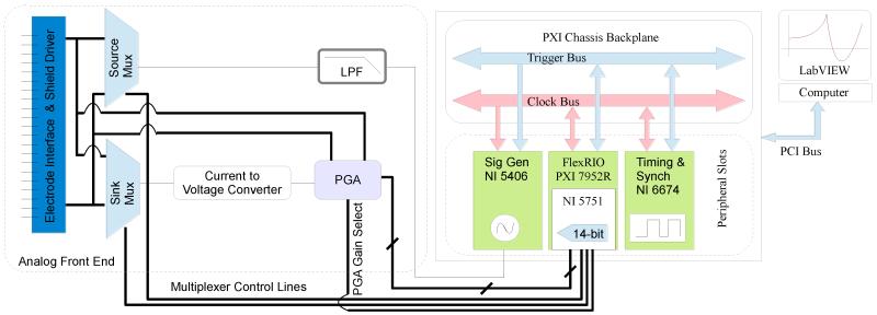
Analog Front End (AFE) : We designed an AFE board with filters, multiplexers for signal switching, Programmable Gain Arrays (PGA), shield drivers, relays for power control etc. on it for appropriate analog conditioning of the signal. The AFE board interfaces with the ADC module, SigGen module and TSync module. The bio-impedance probe is interfaced with the AFE board via front end connectors (shown in blue, on the left end of Figure 1.)
Figure 1.
Block diagram of the EIT system hardware.
3. Software Design
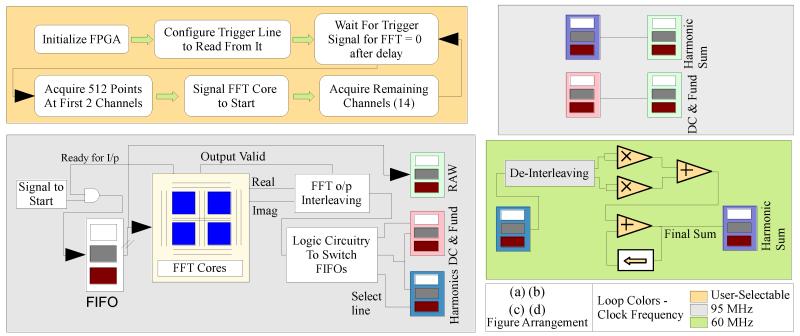
The control software on the computer performs a number of functions including: a) FPGA and ADC module initialization, b) Writing acquisition parameter values in FPGA registers, c) Writing the source-electrode/sink-electrode pattern file in the FPGA memory, d) Triggering start of acquisition, e) Reading data from the FPGA, f) Data calibration and g) Data logging. The FPGA program (realized in hardware, Figure 2) has an initialization circuitry and four blocks performing different functions. These are the Acquisition block, the FFT block, the Spectral Characterization block and the Data Transfer block. Functioning of each block is briefly discussed next.
Figure 2.
FPGA design block diagram
3.1. Acquisition Block
This block reads the ADC registers and writes the values to a First-In-First-Out (FIFO) buffer. It can be clocked using a clock frequency within 30-50 MHz range. The acquisition functions in semi-parallel mode; FPGA acquires samples from 4 channels simultaneously, and then moves on to the next four channels to acquire samples from all other channels.
3.2. FFT Block
This block computes 512-point FFT on the input samples, x, collected from 8 channels and returns X, the real and imaginary component of the FFT output. Since the Acquisition Block and FFT Block work asynchronously, FFT cores use handshaking signals to read from FIFOs used for sharing data between blocks.
3.3. Spectral Characterization Block
We define the Total Harmonic Distortion (THD) of the signal by (1). In this equation, the numerator is the sum of squared magnitude of higher order harmonics, and the denominator is the magnitude squared of the input signal’s dominant harmonic.
| (1) |
We compute the numerator on the FPGA itself and use it to analyze the transient abnormalities or signal quality deterioration. Division is a computationally expensive operation to perform on the FPGA thus the THD is computed on the PC. Calculation of the numerator on FPGA allows us to keep the throughput low, while having a metric to ensure that the signal quality is satisfactory
3.4. Data Transfer Block
DT block queues the transfer of elements from the intermediate FIFOs to the Direct Memory Access (DMA) FIFOs from which PC control software can read the data. DMA FIFOs are implemented using block memory and thus allow simultaneous read and write access and offer deterministic performance across clock domains for loss-less data sharing.
3.5. Averaging Block
Averaging block (not shown in the block diagram) performs signal averaging on the acquired samples before they are read by the FFT block. The averaging block can average at a user-selectable factor up to 64 waveform cycles.
To reduce fabric usage and operation time on the FPGA, design optimizations were performed. The data-sharing blocks were programmed with a pipelined architecture to shorten the longest combinatorial path of gates and were fine-tuned to clock at highest possible clock frequency (without violating timing constraints and determinism), ranging from 50 MHz to 95 MHz.
4. System Characteristics & Future Work
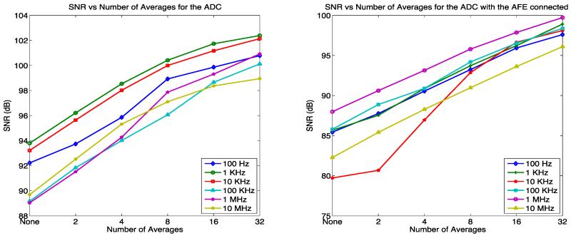
In the current configuration, our system uses 8 channels and a set of 28 source/sink patterns to alternate injecting and sinking electrodes; we are able to record a full spectrum of data (with FFT and spectral characterization, for 47 discrete frequencies spaced logarithmically from 100 Hz to 11.25 MHz, ≈8 Million samples) within 14 seconds. At a fixed signal frequency of 100 KHz, to acquire data from 12 channels for 100 patterns with no signal averaging, the system takes nearly 13ms to do the acquisition, FFT, spectral characterization and calibration. With 28 patterns per frame (or image), this translates to roughly 274 frames (or images) per second, with averaging factor 4; this number drops to 188 frames/sec. Further, by hard coding spectral characterization of the samples on the FPGA itself, we were able to reduce the required throughput between the PC and the FPGA by a factor of 32:1, when compared to the throughput required to transfer all of the samples to the PC. Figure 3 shows the voltage measurement SNR vs. Number of Average plot for 6 different frequencies with and without the AFE connected. For the ADC test, a 2Vpp sinusoidal signal (ADC full-scale) at 100 KHz was applied at the ADC input. For the AFE test, a 2KΩ resistor was connected between a channel and current to voltage converter’s virtual ground. The net gain on the source and sink side was 0.28 and 1.11 respectively (current sense resistor is 499Ω). With input signal set to 2Vpp sine wave at 100 KHz, Vpp at the ADC input was 0.56 V. It can be observed that: 1) Increasing the number of averages improved the SNR (by reducing the Gaussian noise power); 2) With the AFE connected, SNR dropped by about ~4 dBs. In future, we plan to comprehensively evaluate the system performance and to identify and reduce the number of noise sources in it.
Figure 3.
SNR versus number of averages for discrete frequency levels from 6 decades.
Acknowledgments
Research supported by NIH/NCI grant number 1R01CA14302001A1 and NIH/NIBIB grant number 1R21EB011568-01.
References
- [1].McEwan A, et al. Design and calibration of a compact multi-frequency EIT system for acute stroke imaging. Physiol. Meas. 2006;27:199–210. doi: 10.1088/0967-3334/27/5/S17. [DOI] [PubMed] [Google Scholar]
- [2].Oh TI, et al. Validation of a multi-frequency electrical impedance tomography (mfEIT) system KHU Mark1: Impedance spectroscopy and time-difference imaging. Physiol. Meas. 2008;29:295–307. doi: 10.1088/0967-3334/29/3/002. [DOI] [PubMed] [Google Scholar]
- [3].Halter R, et al. A broadband high frequency electrical impedance tomography system for breast imaging. IEEE Trans. On Biomed. Eng. 2008;59:379–390. doi: 10.1109/TBME.2007.903516. [DOI] [PubMed] [Google Scholar]
- [4].Oh TI, et al. A fully parallel multi-frequency EIT system with flexible electrode configuration: KHU Mark2. Physiol. Meas. 2011;32:835–849. doi: 10.1088/0967-3334/32/7/S08. [DOI] [PubMed] [Google Scholar]
- [5].Saulnier GJ. EIT Instrumentation in Electrical Impedance Tomography: Methods, History and Applications. IOP Publishing. 2005:67–104. [Google Scholar]
- [6].Kourunen J, et al. Suitability of a PXI platform for an electrical impedance tomography system. Meas. Sci. and Technol. 2009;20:015503. [Google Scholar]


