Abstract
This paper describes the development and characterization of a high-frequency (65-MHz) ultrasound transducer linear array. The array was built from bulk PZT which was etched using an optimized chlorine-based plasma dry-etching process. The median etch rate of 8 μm/h yielded a good profile (wall) angle (>83°) and a reasonable processing time for etch depths up to 40 μm (which corresponds to a 50-MHz transducer). A backing layer with an acoustic impedance of 6 MRayl and a front-end polymer matching layer yielded a transducer bandwidth of 40%. The major parameters of the transducer have been characterized. The two-way insertion loss and crosstalk between adjacent channels at the center frequency are 26.5 and −25 dB, respectively.
I. Introduction
High-frequency, wideband ultrasound transducer arrays can provide the necessary spatial resolution for applications in dermatology, ophthalmology, and other medical disciplines for which high-quality subsurface imaging is required [1]. Several researchers have focused their efforts on the development of linear and phased arrays operating at high frequencies [2]–[4]. Unlike high-frequency single-element transducers, one of the major challenges in developing high-frequency ultrasound transducer arrays is the patterning of small-scale features within the array. For example, linear arrays designed for 50-MHz operation should have array elements with a pitch of 36 μm and a kerf width of 12 μm. It is almost impossible for conventional fabrication technologies to process elements with such a small kerf.
The most important component of an ultrasonic transducer is the piezoelectric element. There is a wide selection of active materials available for the construction of ultrasound transducer arrays [5]. Navy Type VI (PZT-5H) was selected for this study because it possesses several material properties that are ideal for fabricating high-frequency transducer arrays. This material exhibits good piezoelectric coefficients, high electromechanical coupling, and a high dielectric constant, properties which make PZT-5H an ideal material for building array elements with small element areas. Its low cost also enters favorably into the material selection process.
Conventional arrays are typically manufactured by a dice-and-fill approach, where a PZT plate is separated by mechanical dicing and a polymer is infiltrated and cured within the kerfs. This method can be used to make transducer arrays with frequencies lower than 30 MHz [4]. A composite fabrication method based on the idea of laminating ceramic layers to form a block of composite material has been applied to the development of a 30-MHz ultrasound array [3]. Interdigital pair bonding (IPB) was proposed to fabricate arrays at frequencies up to 50 MHz [6]. Laser micromachining is another method used to fabricate PZT materials [7]–[9].
As an alternative, micromachining techniques can be employed to develop low-cost high-frequency (50 to 100 MHz) ultrasound transducer arrays using mass production. In one batch, hundreds of arrays can be fabricated at one time. The micromachining method can also fabricate kerfs as narrow as a few micrometers. Deep reactive-ion etching (DRIE) has been widely used to etch PZT thin films for ferroelectric memory applications [10]. Recently, new advances in bulk PZT dry etching have been reported [11]–[13]. These authors use pure sulfur hexafluoride (SF6) or a mixture of SF6 and argon (Ar) as etching gases in the plasma etching of PZT. The advantages of fluorine chemistry are its good selectivity to mask materials and its relatively high etch rate, which can reach values as high as 0.25 μm/min. However, because the components of the PZT etch products have significantly higher boiling temperatures, their removal is inefficient. In closely spaced structures, this results in sidewall angles <80°, which is unacceptable for fabricating high-frequency arrays. However, Marks et al. [14] reported that the use of chlorine-based etching gases with an elevated wafer temperature yields good vertical etch profiles and a higher etch rate. The dry-etching mechanism of PZT in chlorinated gas plasmas has been investigated in detail [15], [16], and measures have been proposed to minimize etching damage to the PZT material during the dry-etch process [17]. Using similar dry-etching techniques, researchers have successfully produced array transducers with PZT thick film [18].
In this paper, process parameters for the chlorinated gas plasma have been optimized and applied to bulk PZT etching. High-frequency ultrasound transducer arrays have been designed, fabricated, and characterized. This high-frequency linear array transducer was designed for pre-cancer scanning of skin.
II. Materials and Methods
A. 50-MHz Linear Array Design
Many models have been developed to guide the design of transducer arrays; however, the design of high-frequency transducer arrays is still mostly empirical, generally involving a trial-and-error approach [2]. In this study, we focused on the development of 50 to 100 MHz ultrasound transducer arrays for medical imaging applications within limits set by the micro-fabrication process. Table I lists several key features of the 50-MHz array. Fig. 1 shows the layout of the transducer array. To validate the array design, both PZFlex (Weidlinger Associates Inc., Mountain View, CA) and Field II [19], [20] modeling were carried out. The PZFlex program was used to predict the azimuthal beam profile for 8 elements to investigate the impact of grating lobes. Because the element-to-element spacing was around 1.5λ, a transmitting grating lobe was expected near 40° as shown in Fig. 1(b).
TABLE I.
Initial Design Goals and Some Key Features of the Array.
| Center frequency | 50 MHz |
| Element-to-element pitch | 36 μm |
| Kerf between elements | 12 μm |
| Number of elements | 32 |
| Element length | 4 mm |
| Bandwidth | >50% |
Fig. 1.
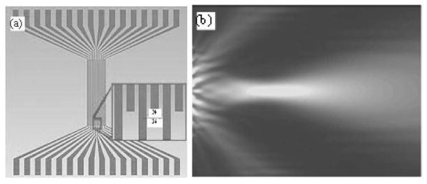
(a) Layout of one transducer array for 50 MHz and (b) simulated pressure pattern using PZFlex.
B. Fabrication of Bulk PZT Ultrasound Linear Arrays
The fabrication procedure illustrated in Fig. 2 was used to build all of the transducer arrays in this study. A bulk PZT-5H (CTS Corp., Bloomingdale, IL) wafer with a thickness of 500 μm was double-sided lapped and then polished on one side.
Fig. 2.
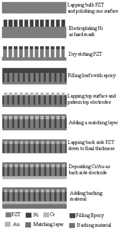
Schematic process flow for micromachining bulk PZT ultrasound transducer arrays.
A thin layer of nickel was sputtered onto the polished side as a seed layer for subsequent electroplating. A photolithography-based method was then applied to transfer design patterns onto the PZT surface. First, a thick positive photoresist layer was spin-coated onto the PZT. After baking on a hot plate at 100°C for 5 min, the photoresist was exposed directly by a laser writer (DWL66, Heidelberg Instruments Mikrotechnik GmbH, Heidelberg, Germany). The wafer was dipped in photoresist developer for developing. The patterned photoresist structures were then formed. Next, the Ni electroplating process was run to form a 6-μm-thick Ni hard mask through the openings of the photoresist pattern. To obtain a dense Ni layer in the small open areas, a pulse power supply (Dynatronix Inc., Amery, WI) was used to provide pulses (0.1 ms on and 0.9 ms off) with the average current 20 mA/cm2. After electroplating, the photoresist was stripped off using acetone. The PZT wafer with Ni hard mask was etched with chlorine-based gas plasma.
After dry etching of the PZT material, the kerfs were infiltrated with Epo-Tek 301–2 epoxy (Epoxy Technology Inc., Billerica, MA). The epoxy was cured in an oven at an elevated temperature of 60°C overnight. The wafer was then lapped on the etched side until the PZT structures were exposed. Layers of Cr and Au were deposited onto this side and patterned to form the top electrodes using photolithography techniques. The wafer was flipped over to the other side and lapped until the designed thickness was reached. Conductive E-Solder 3022 (Von Roll Isola Inc., New Haven, CT) was used as a backing material. Parylene (Specialty Coating Systems, Indianapolis, IN) was used for the only matching layer at the front of the transducer.
A flexible circuit was selected to connect each array element electrically. To lower the noise level, a multi-layer flexible circuit with one layer of ground was designed and fabricated. After alignment, each end of the array was bonded to a flexible circuit. The two flexible circuits were then bonded to a PCB connector with epoxy. Coaxial cables were connected to the array via the PCB board and flexible circuits. Finally, the array was housed in a brass tube and sealed with an insulated epoxy material. The transducers were then ready for testing.
C. Characterization of the Ultrasound Linear Array
First, the arrays were poled at around 30 KV/cm for 10 min. The dielectric constant and dielectric loss for all 32 elements were measured by using an RF impedance/material analyzer (3094A, Agilent Technologies Inc., Santa Clara, CA). Effective electromechanical coupling coefficients were derived from the measured impedance curve.
All of the transducers were tested in a degassed, deionized water tank in pulse-echo mode by reflecting the signal off an X-cut quartz target. Pulse-echo response, insertion loss, and crosstalk between adjacent elements were measured using a previously described experimental arrangement [4].
III. Results and Discussion
Etching rate, selectivity ratio, and profile angle are the most important parameters when dry etching bulk PZT for the construction of high-frequency ultrasound transducer arrays. By optimizing ICP power, substrate power (controlling substrate dc bias voltage), and the flow rates and ratios of the etching gases, we found that a median etching rate of 8 μm/h was a suitable value for the process. It took too much time to achieve the final thickness at lower etch rates, and higher etch rates lead to deterioration of the profile angle. Finally, we used an inductively coupled plasma reactive-ion etching system (Plasmatherm SLR770 ICP system, Unaxis Inc., Irvine, CA) employing Cl2/Ar-based chemistry for the etching process. To achieve an etching rate for bulk PZT of 8 μm/h, we used 600 W of ICP power, dc bias voltage of 200 V, 20 sccm of Ar, and 60 sccm of Cl2.
The etching selectivity of bulk PZT to Ni was about 20:1 in this study. Fig. 3 shows an array pattern with an etch depth of 40 μm, which required about 5 h of processing. The sidewall angle is about 83°. The effect of the slope of the elements on the performance of the transducer has been studied [21]. The kerf is still open with a width of more than 2 μm at the bottom. After lapping, the final thickness of the PZT material was 32 μm.
Fig. 3.
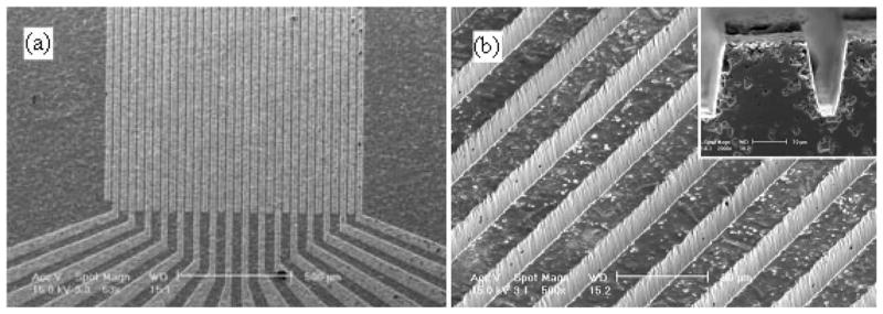
Scanning electron micrographs of etched bulk PZT array structures (a) top view; (b) 45° view with a cross-sectional view embedded.
Fig. 4 shows how the transducer was bonded using two flexible circuits. On the flexible circuit, Cr/Au metal film was coated and patterned. The metal traces were expanded from one end and bonded to the array at the other end, which was bonded to a PCB board. After the transducer was assembled, it was characterized.
Fig. 4.
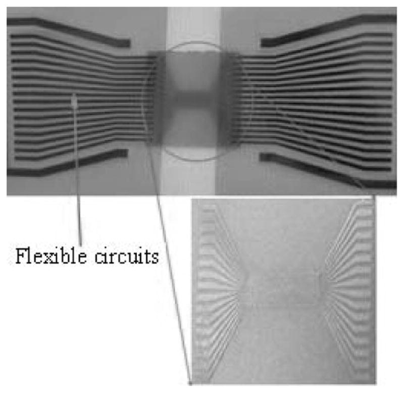
Photograph of flexible circuits wire-connected with the linear arrays.
The electric impedance was measured and is shown in Fig. 5(a). The center frequency was 65 MHz. The calculated electromechanical coupling coefficient from Fig. 5 was 0.53, which is lower than that for the bulk PZT material. The pulse-echo response and frequency spectrum of the array were experimentally measured; the results are given in Fig. 5(b). The measured pulse-echo response was obtained for one element of a 65-MHz transducer array. As mentioned previously, the front-end matching layer was 9-μm Parylene. The acoustic impedance of the E-Solder backing layer (6 MRayls) is relatively low compared with that of bulk PZT. As a result, the −6 dB bandwidth of the transducer was about 40%.
Fig. 5.
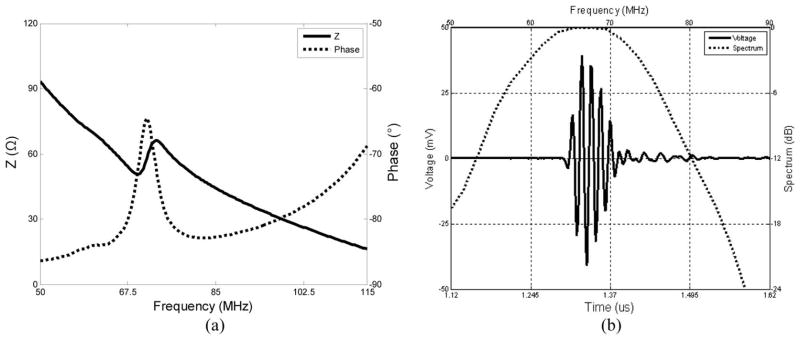
Experimental results of (a) electric impedance and (b) pulse-echo response of one typical array element.
The two-way insertion loss was 26.5 dB at a center frequency of 65 MHz. The crosstalk between adjacent channels is about −25 dB at the center frequency. The pulse-echo test results for the array are summarized in Table II.
TABLE II.
Measured Properties of the 32-Element Linear Array.
| Number of elements | 32 |
| Average center frequency | 65.6 MHz |
| High/low center frequencies | 67.8 MHz/63.5 MHz |
| Average bandwidth | 41% |
| −20 dB pulse length | 135 ns |
| Crosstalk between adjacent elements | −25 dB |
IV. Conclusions
Linear arrays made from micromachining bulk PZT at frequencies over 50 MHz have been developed using a DRIE dry-etching technique. The arrays consist of 32 elements with an element width of 24 μm and a kerf width of 12 μm. The element length is 4 mm, and the thickness is approximately 32 μm. Values for the −6-dB bandwidth and two-way insertion loss are about 40% and 26 dB, respectively. The crosstalk between adjacent channels is about −25 dB at the center frequency.
Acknowledgments
The authors would like to acknowledge J. Williams and Dr. J. Cannata for their assistance in the transducer fabrication process.
This work was supported by the National Institutes of Health grant P41-EB2182.
Contributor Information
Changgeng Liu, Email: cliu@geospace-research.com, Geospace Research Inc., El Segundo, CA.
Qifa Zhou, Department of Biomedical Engineering, University of Southern California, Los Angeles, CA.
Frank T. Djuth, Geospace Research Inc., El Segundo, CA
K. Kirk Shung, Department of Biomedical Engineering, University of Southern California, Los Angeles, CA.
References
- 1.Lockwood G, Turnbull H, Christopher D, Foster F. Beyond 30 MHz. IEEE Eng Med Biol Mag. 1996;15(6):60–71. [Google Scholar]
- 2.Shung K, Zipparo M. Ultrasonic transducers and arrays. IEEE Eng Med Biol Mag. 1996;15(6):20–30. [Google Scholar]
- 3.Ritter T, Shrout TR, Tutwiler R, Shung KK. A 30-MHz piezo-composite ultrasound array for medical imaging applications. IEEE Trans Ultrason Ferroelectr Freq Control. 2002;49(2):217–230. doi: 10.1109/58.985706. [DOI] [PubMed] [Google Scholar]
- 4.Cannata J, Williams JA, Zhou QF, Ritter TA, Shung KK. Development of a 35-MHz piezo-composite ultra-sound array for medical imaging. IEEE Trans Ultrason Ferroelectr Freq Control. 2006;53(1):224–236. doi: 10.1109/tuffc.2006.1588408. [DOI] [PubMed] [Google Scholar]
- 5.Shung K, Cannata J, Zhou Q. Piezoelectric materials for high frequency medical imaging applications: A review. J Electroceram. 2007;19(1):139–145. [Google Scholar]
- 6.Liu R, Knapik D, Harasiewics KA, Foster FS. Fabrication of 2-2 piezocomposites by interdigital pair bonding. Proc IEEE Ultrasonics Symp. 1999;2:973–976. [Google Scholar]
- 7.Lukacs M, Sayer M, Lockwood G, Foster S. Laser micromachined high frequency ultrasonic arrays. Proc IEEE Ultrasonics Symp. 1999:1209–1212. [Google Scholar]
- 8.Farlow R, Galbraith W, Knowles M, Hayward G. Micromachining of a piezocomposite transducer using a copper vapor laser. IEEE Trans Ultrason Ferroelectr Freq Control. 2001;48(3):639–640. doi: 10.1109/58.920684. [DOI] [PubMed] [Google Scholar]
- 9.Tanaka K, Konishi T, Ide M, Meng ZC, Sugiyama S. Fabrication of microdevices using bulk ceramics of lead zirconate titanate. Jpn J Appl Phys. 2005;44(9B):7068–7071. [Google Scholar]
- 10.Kokaze Y, Kimura I, Endo M, Ueda M, Kikuchi S, Nishioka Y, Suu K. Dry etching process for Pb(Zr, Ti)O3 thin-film actuators. Jpn J Appl Phys. 2007;46(1):280–282. [Google Scholar]
- 11.Bale M, Palmer R. Deep plasma etching of piezoelectric PZT with SF6. J Vac Sci Technol B. 2001;19(6):2020–2025. [Google Scholar]
- 12.Wang S, Li X, Wakabayashi K, Esashi M. Deep reactive ion etching of lead zirconate titanate using sulfur hexafluoride gas. J Am Ceram Soc. 1999;82(5):1339–1341. [Google Scholar]
- 13.Subasinghe S, Goyal A, Tadigadapa S. High aspect ratio plasma etching of bulk lead zirconate titanate. Proc SPIE. 2006;6109:art. no. 61090D. [Google Scholar]
- 14.Marks S, Almerico JP, Gay MK, Celii FG. The profile and device characterization of high wafer temperature etched Ir/PZT/Ir stacks. Integr Ferroelectr. 2003;59(1):333–340. [Google Scholar]
- 15.Jung J, Lee W. Dry etching characteristics of Pb(Zr, Ti)O3 films in CF4 and Cl2/CF4 inductively coupled plasmas. Jpn J Appl Phys. 2001;40(1):1408–1419. [Google Scholar]
- 16.Efremov A, Kim D, Kim C. Etching mechanism of Pb(Zr, Ti)O3 thin films in Cl2/Ar plasma. Plasma Chem Plasma Process. 2004;24(1):13–28. [Google Scholar]
- 17.Kang M, Kim K, Kim D, Kim C. Reduction of dry etching damage to PZT films etched with a Cl-based plasma and the recovery behavior. J Korean Phys Soc. 2002;41(4):445–450. [Google Scholar]
- 18.Zhou QF, Wu DW, Liu CG, Zhu BP, Djuth F, Shung KK. Micromachined high-frequency (80 MHz) PZT thick film linear arrays. IEEE Trans Ultrason Ferroelectr Freq Control. 57(10):2213–2220. doi: 10.1109/TUFFC.2010.1680. [DOI] [PMC free article] [PubMed] [Google Scholar]
- 19.Jensen JA. Field: A program for simulating ultrasound systems. Med Biol Eng Comput. 1996;34(suppl 1, pt 1):351–353. [Google Scholar]
- 20.Jensen JA, Svendsen NB. Calculation of pressure fields from arbitrarily shaped, apodized, and excited ultrasound transducers. IEEE Trans Ultrason Ferroelectr Freq Control. 1992;39(2):262–267. doi: 10.1109/58.139123. [DOI] [PubMed] [Google Scholar]
- 21.Yuan JR, Jiang X, Cao P-J, Sadaka A, Bautista R, Snook K, Rehrig PW. High frequency piezo composites microfabricated ultrasound transducers for intravascular imaging. Proc IEEE Ultrasonics Symp. 2006:264–268. [Google Scholar]


