Abstract
We report, for the first time, the use of a single step deposition of semiconductor channel layer to simultaneously achieve both n- and p-type transport in transparent oxide thin film transistors (TFTs). This effect is achieved by controlling the concentration of hydroxyl groups (OH-groups) in the underlying gate dielectrics. The semiconducting tin oxide layer was deposited at room temperature, and the maximum device fabrication temperature was 350°C. Both n and p-type TFTs showed fairly comparable performance. A functional CMOS inverter was fabricated using this novel scheme, indicating the potential use of our approach for various practical applications.
Thin film transistors (TFTs) based on transparent metal oxide semiconductors have emerged as the ideal candidates for pixel-switching in flat-panel display (FPD) applications1. Significant progress has been accomplished in n-channel TFTs performance using various metal oxide semiconducting thin films as the channel layers, prepared by both physical2,3,4 and chemical route deposition techniques5,6,7. Prototypes of flat-panel displays using TFTs based on oxide semiconductors have been recently demonstrated by several research groups8,9. Although, n-channel oxide TFTs are suitable for pixel-switching in next generation FPDs, p-channel oxide-based TFTs may still be required for the realization of many types of low power circuits10. Complementary metal oxide semiconductor (CMOS) inverters comprising both p- and n-type TFTs are the basic building blocks for complex integrated circuits for system-on-chip and other electronic applications. It is noted that, most of the reported metal oxide complementary circuits are based on single carrier n-type oxide TFTs11,12. However, the single carrier type inverters possess a relatively small input capacitance and have low output swing, leading to a large power dissipation and poor noise margin. As an alternative, hybrid n-type oxide and p-type organic TFTs have been used for the fabrication of complementary type inverters13,14. However, the complex fabrication process of p-channel organic TFTs compared to the n-channel oxide based TFTs inhibits the use of hybrid inorganic-organic CMOS inverters for practical applications. Although, few articles have been published on cuprous oxide (Cu2O)15,16,17 and tin monoxide (SnO)18,19,20 based p-channel TFTs, fabrication of CMOS inverters using these p-channel oxide TFTs along with the well-established n-type oxide TFTs has not been explored. The compatibility of process temperature and growth conditions of n- and p-type oxide semiconductor thin films is a major issue to integrate them for the development of CMOS inverters.
In this work, we report, for the first time, the fabrication of a transparent oxide CMOS inverter device using a single step deposited tin oxide thin film channel layer at a low processing temperature of 210°C. Our approach is very unique, as it uses a single host semiconductor film which can be tuned either n- or p-type by just controlling the OH-group concentration in the gate dielectrics. The resulting n- and p-channel TFTs using these tin oxide semiconducting channel layers showed reasonable electrical performance and were successfully utilized to fabricate CMOS inverters. In case of conventional CMOS fabrication process a single dielectric and two different semiconductor materials are normally used. However, if the process conditions of the p- and n- type semiconductors are not compatible then it is very difficult to integrate them in a single device. In such cases, our approach is more attractive even though it involves the same number of steps. The development of this one-step deposition of n- and p-type tin oxide semiconductor holds promise for the realization of more complex, power-efficient transparent circuits.
Results
Device perfromance
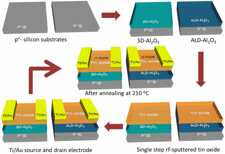
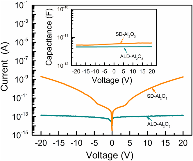
The process flow for the realization of both n- and p-channel TFTs from a single tin oxide semiconductor channel layer deposition is shown in Figure 1. The process uses solution derived aluminum oxide (SD-Al2O3) and atomic layer deposited aluminum oxide (ALD-Al2O3), respectively, as the gate dielectrics. Figure 2 shows the current vs volatge characteristics of the dielectric films measured with p+-Si/ALD-Al2O3/Au and p+-Si/SD-Al2O3/Au structures. The inset to Figure 2 shows the capacitance vs volatge characteristics of the two dielectric films measured at 1 MHz frequecny. The capacitance vs voltage characteristics exhibited the typical behavior of a metal-insulator-metal (MIM) capacitor21. The average capacitance of the ALD-Al2O3 and SD-Al2O3 were found to be ~60 nFcm−2 and ~75 nFcm−2, respectively.
Figure 1. Simultaneous n- and p-channel TFT fabrication.
Process flow of n- and p-type channel TFT fabrication using single step deposited tin oxide semiconducting film on SD-Al2O3 and ALD-Al2O3 gate dielectrics, respectively.
Figure 2. I-V and C-V characteristics of the dielectrics.
Current vs volatge characteristics of the aluminum oxide films measured with p+-Si/ALD-Al2O3/Au and p+-Si/SD-Al2O3/Au structures. The inset shows the capacitance vs volatge characteristics of the two aluminum oxide films measured at 1 MHz frequecny.
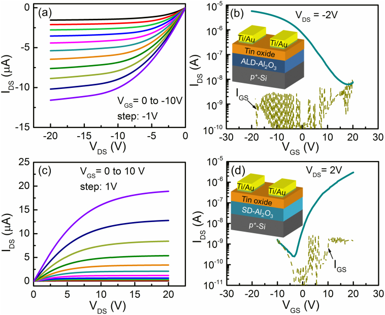
The electrical properties of the n- and p-channel TFTs are shown in Figure 3(a–d). A schematic illustration of individual TFT devices using ALD-Al2O3 and SD-Al2O3 gate dielectrics are shown in the insets to Figure 3(b) and (d), respectively. The output characterstic of the TFT using ALD-Al2O3 as gate dielectric shown in Figure 3(a), show p-type conductivity of the tin oxide film deposited on ALD-Al2O3, since the holes are generated at negative gate voltages (VGS). Interestingly, the output characterstic of the TFT using SD-Al2O3 as gate dielectric shown in Figure 3(c), indicate n-type behavior of the tin oxide film deposited on SD-Al2O3, since the electrons are generated at positive VGS. Both the devices showed well saturated output characteristics. The absence of current crowding at low source-to-drain voltage (VDS) region indicates the existence of an ohmic contact between Ti/Au and the tin oxide film deposited on both gate dielectrics. The measured non-zero drain current at zero applied VGS in case of the TFT using ALD-Al2O3 as gate dielectric indicates that the p-channel tin oxide TFT operates in the depletion mode. However, the n-channel tin oxide TFT using SD-Al2O3 as gate dielectric was found to be operating in the enhancement mode, with zero drain current, measured at zero applied VGS.
Figure 3. Performance of n- and p-channel tin oxide TFTs.
(a) Output and transfer (b) characteristic of tin oxide p-channel TFTs using ALD-Al2O3 as gate dielectric. Output (c) and transfer (d) characteristic of tin oxide n-channel TFTs using SD-Al2O3 as gate dielectric.
The transfer characteristics were obtained in the linear region of operation at a constant VDS of −2 V and +2 V for the TFTs using ALD-Al2O3 (Figure 3(b)) and SD-Al2O3 (Figure 3(d)) as the gate dielectrics, respectively. Linear-region field-effect mobility (μlin) and threshold voltage (VT) and drain on-current to off-current ratio (Ion/Ioff) were calculated from the transfer characteristics shown in Figure 3(b) and (d), respectively. The p-channel TFT with ALD-Al2O3 as gate dielectric showed a μlin of 0.42 cm2V−1s−1 with a VT of 2.5 V and Ion/Ioff of ~103. The value of μlin, VT and Ion/Ioff for the n-channel TFT with SD-Al2O3 as gate dielectric were estimated to be 0.52 cm2V−1s−1, 10.8 V and Ion/Ioff of ~104, respectively. It should be noted that the mobility of these devices is not as high as previously reported by our group18. This fact is due to the different gate dielectric used here, and the fact that the temperature at which we could simultaneously achieve both n and p-type behavior is not necessarily the optimal temperature to get highest mobility for either conduction polarity. We believe the mobility and Ion/Ioff ratio of the devices can be improved by further device engineering, using other gate dielectrics, or controlling the semiconductor thickness. However, the key point here is that, although the tin oxide films were prepared simultaneously on ALD-Al2O3 and SD-Al2O3 gate dielectrics under same deposition and annealing conditions, the resulting devices exhibits different charge carrier polarity. In other words, the same tin oxide film deposited on ALD-Al2O3 exhibits p-type semiconductor characteristics, whereas, the tin oxide film deposited on SD-Al2O3 exhibits n-type semiconductor characteristics. It may be noted that the devices using as-deposited tin oxide films on SD-Al2O3 and ALD-Al2O3 did not show any (n-/p-type) TFT characteristics, and working devices were only obtained after annealing. As the tin oxide films were deposited at the same time and the samples were annealed simultaneously, we concluded that the change in tin oxide from p to n-type is caused by the dielectric layer. Based on the material characteristics of both types of aluminum oxide films, we found an abundant presence of OH-groups in the SD-Al2O3 which we believe is the source of extra oxygen that helps to form a tin dioxide film with n-type characteristics.
Material characterization
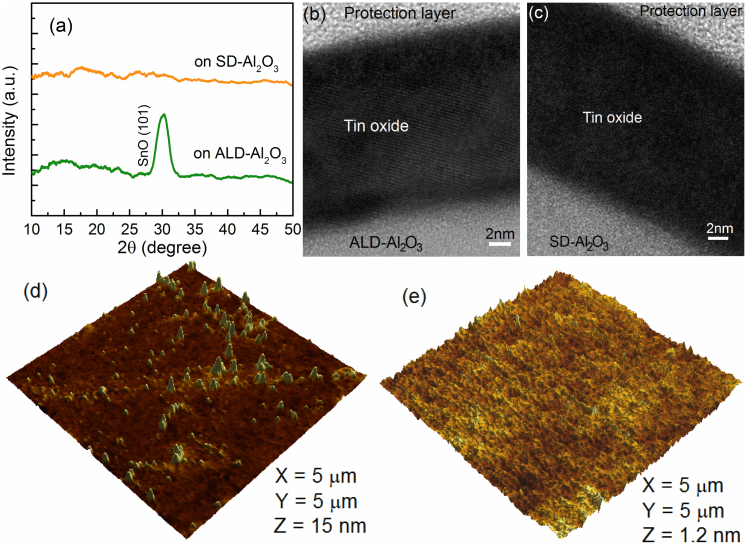
For material characterizations, tin oxide films were prepared on ALD-Al2O3 and SD-Al2O3 under the same deposition conditions, as used in case of TFT fabrication. Figure 4(a) shows the x-ray diffraction (XRD) patterns of the tin oxide films deposited on both types of gate dielectrics using grazing-incidence geometry with a fixed incident angle of 1°. The XRD pattern of the tin oxide film deposited on ALD-Al2O3 reveals a crystalline structure, with a Bragg's peak corresponding to the (101) reflection of tin monoxide (SnO)18. The absence of any other peaks of SnO in this case suggests the preferential orientaion of crystallites along the [101] direction. Interestingly, however, no Bragg's peaks were found in case of the tin oxide film deposited on SD-Al2O3, suggesting an amorphous nature of the corresponding film. High resolution cross-sectional transmission electron microscope (TEM) images were obtained to further investigate the crystallinity of aforementioned tin oxide films. Clear lattice fringes were observed in case of the TEM image of the tin oxide film deposited on ALD-Al2O3 (Figure 4 (b)), confirming the formation of crystalline tin monoxide film on ALD-Al2O3. The measured interplanar spacing (d) was found to be ~3.02 Å which is close to the reported d-value (2.986 Å) of (101) planes of tin monoxide (SnO) (JCPDS card No. 00-006-0395). The appearance of well-defined lattice fringes corresponding to only (101) planes confirms the preferential orientation of tin oxide crystallites along the [101] direction and is consistent with the XRD results. However, no lattice fringes were observed in case of the tin oxide film deposited on SD-Al2O3 (Figure 4(c)), which is consistent with the XRD results, and confirms the amorphous nature of the corresponding tin oxide film. Figure 4(d) and (e) show the atomic force microscope images of the tin oxide films deposited on ALD-Al2O3 and SD-Al2O3, respectively. The root-mean-square (rms) surface roughness of the bare ALD-Al2O3 and SD-Al2O3 films were found to be ~0.4 nm and ~0.2 nm, respectively (results are not shown here). However, the rms surface roughness of the tin oxide film depsoited on ALD-Al2O3 (~0.9 nm) was found to be higher than that of the tin oxide film depsoited on SD-Al2O3 (~0.3 nm), which can be attributed to the crystalline nature of the former.
Figure 4.
Properties of tin oxide films on ALD-Al2O3 and SD-Al2O3 (a) XRD patterns of the tin oxide films deposited on Si/ALD-Al2O3 and Si/SD-Al2O3. High resolution cross-sectional TEM images of tin oxide films deposited on (b) Si/ALD-Al2O3 and (c) Si/SD-Al2O3. AFM images of tin oxide films deposited on (d) Si/ALD-Al2O3 and (e) Si/SD-Al2O3.
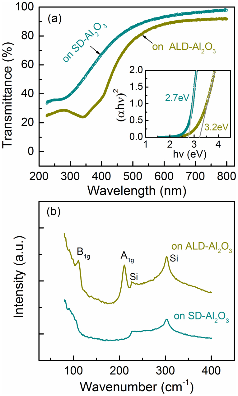
The UV-VIS transmittance spectra of the tin oxide films deposited on glass/ALD-Al2O3 and glass/SD-Al2O3 are shown in Figure 5(a). The transparency of the tin oxide film deposited on SD-Al2O3 is higher than that of the tin oxide film deposited on ALD-Al2O3. The optical bandgap, Eg, was estimated by extrapolating the linear portion of the (αhν)2 vs hν plot as shown in the inset to Figure 5(a), where α is the absorption coefficient and hν is the incident photon energy. The estimated value of Eg for the tin oxide film deposited on ALD-Al2O3 was found to be ~2.7 eV, which is well consistent with the reported optical band gap of tin monoxide (SnO)18,20. Interestingly, the value of Eg for the tin oxide film deposited on SD-Al2O3 was found to be ~3.2 eV, which is close to the optical band gap (~3.6 eV) of tin dioxide (SnO2)22. Raman spectra of the tin oxide films deposited on Si/ALD-Al2O3 and Si/SD-Al2O3 are shown in Figure 5(b). The Raman spectra of the tin oxide film deposited on ALD-Al2O3 shows two peaks, one at ~111.2 cm−1 and another at ~211 cm−1 corresponding to the A1g and B1g mode of vibrations of tin monoxide, respectively23,24. The peaks at 226.5 cm−1 and 302.8 cm−1 belong to the silicon substrate. Interestingly, no peaks were observed in case of the tin oxide film deposited on SD-Al2O3, the absence of A1g and B1g peaks in the measured wavenumber range have been reported to be a signature of conversion of SnO to SnO2 phase23. From the TFT and material characterization results, it is clearly observed that although the tin oxide films were prepared simultaneously under same deposition and annealing conditions, however, different phases of tin oxide are formed on ALD-Al2O3 and SD-Al2O3 films. Thus, it is important to investigate the chemical composition of ALD-Al2O3 and SD-Al2O3 films, which are solely responsible for the different tin oxide phase formation.
Figure 5.
Optical properties of tin oxide films (a) UV-VIS spectra of tin oxide films deposited on glass/ALD-Al2O3 and glass/SD-Al2O3. (b) Raman spectra of tin oxide films deposited on Si/ALD-Al2O3 and Si/SD-Al2O3. Excitation wavelength of 473 nm laser was used for the Raman spectra measurements.
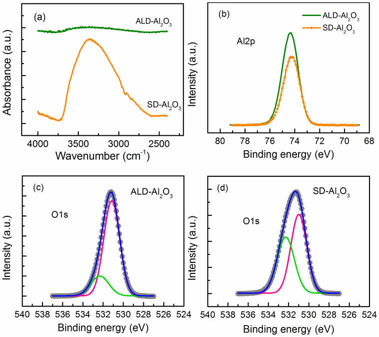
Fourier transform infrared (FT-IR) spectroscopy and x-ray photoelectron spectroscopy (XPS) tests of the bare ALD-Al2O3 and SD-Al2O3 films deposited on silicon substrates were performed to investigate their chemical composition and to understand their effects on different tin oxide phase formation. Figure 6(a) shows the FT-IR spectrums of the ALD-Al2O3 and SD-Al2O3 films in the wavenumber range of 4000 cm−1 to 2400 cm−1. In case of the ALD-Al2O3 film, a very weak and broad peak was observed in the wavenumber range of 3750 cm−1 to 2600 cm−1. However, a very intense and broad peak centered at 3368 cm−1 corresponding to the stretching vibration of the OH-group25 was observed in case of the SD-Al2O3 film, indicating the presence of a large number of OH-groups. The presence of large amount of OH-in the SD-Al2O3 gate dielectric is believed to be due to water absorbed from the environment into the solution-derived aluminum oxide films (SD-Al2O3) after the final annealing treatment and subsequent exposure to air. It is expected that the SD-Al2O3 film crystallized at 350°C is not completely oxidized, which make more prone to water absorption from ambient after annealing. Evidence for this conclusion can be found in the fact that the intensity of the aformentioned FT-IR peak (at ~3368 cm−1) was found to dcrease significantly with increasing SD- Al2O3 annealing tempearature ≥500°C.
Figure 6. FT-IR and XPS spectra of aluminum oxide dielectrics.
(a) FT-IR spectra of ALD-Al2O3 and SD-Al2O3 thin films, (b) XPS Al2p peaks of ALD-Al2O3 and SD-Al2O3 thin films, XPS O1s peak of ALD-Al2O3 (c) and SD-Al2O3 thin films.
The XPS Al2p peaks of the ALD-Al2O3 and SD-Al2O3 films are shown in Figure 6(b). A single Al2p peak at ~74.4 eV and ~74.3 eV was found in case of the ALD-Al2O3 and SD-Al2O3, respectively. The appearance of Al2p peak at lower binding energy in case of the SD-Al2O3 compared to the ALD-Al2O3, may be attributed to the incomplete oxidation of the SD-Al2O3 film as evident from the FT-IR results. XPS O1s peaks of the ALD-Al2O3 and SD-Al2O3 are shown in Figure 6(c) and (d), respectively. The open circles show the measured data and the solid lines represents the Gaussian peak fitting results. In both cases, the deconvolution of O1s peak exhibited one peak at ~531.0 eV, attributed to the O−2 in Al2O3 and another peak at ~532.3 eV, attributed to oxygen associated to the OH− in aluminum hydroxide26.Interestingly, however, the intensity of the peak at ~532.3 eV in case of the SD-Al2O3 was found to be significantly higher than that of the ALD-Al2O3, suggesting the presence of a large number of OH-groups in the former case and this observation is well consistent with the FT-IR results.
Considering the FT-IR and XPS results of ALD-Al2O3 and SD-Al2O3 films, the formation of different tin oxide phases can be explained as follows. It is important to note that, the tin oxide films were simultaneously deposited on both ALD-Al2O3 and SD-Al2O3 and all the films were subjected to thermal annealing together at the same temperature. It has been reported that tin monoxide (SnO) is a metastable phase and it can easily transform to tin dioxide (SnO2) phase in the presence of excess oxygen and temperature by the local disproportionate redistribution of internal oxygen18,27. Thus, we believe that the large number of OH-groups present in the SD-Al2O3 film act as additional oxygen source during annealing, which helps to convert the metastable SnO phase to an n-type amorphous SnO2 phase. In contrast, tin oxide films deposited on ALD-Al2O3 remain as SnO phase with p-type semiconductor characteristics, due to the presence of very negligible OH-content in the ALD-Al2O3 film. It has been reported that tin vacancies are the most likely defects that are responsible for the p-type conduction in tin monoxide film18,19,28. Whereas, oxygen vacancies are the dominant defects responsible for n-type conduction in tin dioxide29. Although, the OH-groups in the SD-Al2O3 provided the extra oxygen to form a tin dioxide phase as observed from the UV-VIS and Raman spectroscopy results, we believe that a sufficiently large concentration of oxygen vacancies remain in the SnO2 film, which cause the n-type channel conduction in case of the tin oxide film deposited on SD-Al2O3.
Performance of CMOS inverter
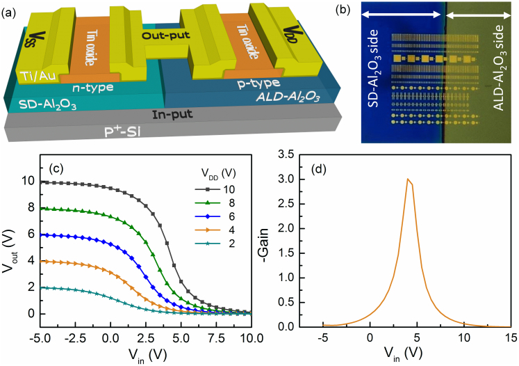
Having established the fabrication of n- and p-channel TFTs from a single step deposition of tin oxide film, we took advantage of this novel finding to fabricate functional CMOS inverters. Figure 7(a) shows the conceptual design of the CMOS inverter device used in this study and Figure 7(b) shows the top-view optical image of the actual sample having both n-channel TFTs in the left hand side (on SD- Al2O3) and p-channel TFTs in the right hand side (on ALD-Al2O3) on a single p+-Si substrate. The common gate (p+-Si) electrode was used as the input terminal (Vin) of the CMOS inverter. The drain of the n-channel TFT and source of the p-channel TFT were connected together and was used as the output terminal (Vout) of the CMOS inverter. The voltage transfer curves of the CMOS inverter measured at different supply voltages (VDD) as shown in Figure 7(c), exhibited typical response of an inverter. The fabricated complementary inverter exhibited a gain (−∂Vin/∂Vout) of ~3 (Figure 7(d)). While this gain is admittedly low, the fabricated devices clearly demonstrate the validity of our novel approach for simultaneous formation of n- and p-type tin oxide thin film channel layers. The gain of these inverters may be increased by using appropriate channel dimensions of the n- and p-channel TFTs, further optimization of the tin oxide film process, and using another gate dielectric.
Figure 7.
Performance of CMOS inverter (a) Conceptual CMOS inverter device structure and (b) top-view image of the actual sample with both n- and p-type tin oxide TFTs used for CMOS inverter measurements. (c) Voltage transfer and (d) gain characteristics of the CMOS inverter.
Discussion
A novel single step deposited tin oxide thin film is used to achieve both n- and p-type channel layers using Al2O3 dielectrics deposited by two different routes. Our study reveals that the presence of OH-groups in the solution derived aluminum oxide dielectric layer is responsible for the formation of an amorphous tin dioxide phase, with a very stable n-type semiconductor characteristic. In contrast, tin monoxide phase with p-type semiconductor characteristics, is formed on ALD deposited aluminum oxide (or other dielectric films having no or very less amount of OH-groups). Compared to the previously reported growth processes of individual n- or p-type semiconducting thin films, our approach is very advantageous since both n- and p-type channel layers can be prepared in a single step deposition process using the same host tin oxide semiconducting film.
In conclusion, we have reported a novel approach for the formation of both n and p-channel layers, using a single semiconductor layer deposition step. A functional CMOS inverter was successfully fabricated, demonstrating the feasibility of our approach. The realization of this simple process for transparent oxide CMOS is an important step in the development of power-efficient transparent circuits.
Methods
Aluminum oxide thin film preparation
Aluminum oxide dielectric thin films were deposited on heavily doped p-type silicon substrates using atomic layer deposition and spin coating techniques. The atomic layer deposited aluminum oxide (ALD-Al2O3) thin films (120 nm) were prepared at 200°C by a Cambridge Nanotech ALD system using trimethylaluminum and water as precursors. The solution-derived aluminum oxide (SD-Al2O3) thin films (~110 nm) were deposited by spin coating technique at 350°C, details of the deposition process can be found elsewhere30.
n- and p-channel tin oxide TFT fabrication
Tin oxide thin films were deposited simultaneously on aforementioned ALD-Al2O3 and SD-Al2O3 by direct current (DC) reactive magnetron sputtering (Angstrom Science, Canada) using 2 inch tin metal target (purity ~99.99%). The reactive DC sputtering was performed at room temperature using a mixture of argon and oxygen gases with oxygen partial pressure (Opp) of 9% and at a deposition pressure of 1.8 mTorr. A bilayer of titanium (10 nm) and gold (70 nm) source and drain electrodes were deposited on top of the tin oxide film using shadow mask and e-beam evaporation. The channel width (W) and length (L) of the TFTs were fixed as 500 μm and 100 μm, respectively. Then the devices were subjected to thermal annealing at 210°C for about 30 min using a tube furnace in air atmosphere. For material characterizations, tin oxide thin films without Ti/Au were prepared under similar deposition conditions. To decrease the gate to source leakage current (IGS) and to minimize the current due to electric fringing effects, the tin oxide semiconductor layer was mechanicaly scratched to create individual channel pads of size ~550 μm × ~300 μm, which led to a low IGS of ~10−9 A in the entire sweeping range in both cases of n- and p-type tin oxide TFTs.
CMOS fabrication
ALD-Al2O3 was first deposited on a p+-Si substrate and then SD-Al2O3 was deposited on the half portion of the same p+-Si substrate using Kapton-tape as protection mask. Tin oxide and Ti/Au thin films were then deposited under similar conditions of TFTs as mentioned above and then the whole device was subjected to annealing at 210°C for 30 min in air.
Material and device characterizations
Fourier transform infrared spectra (FT-IR) of the aluminum oxide films were obtained by a Nicolet iS10 FT-IR (Thermo Scientific) Spectrometer. Crystallinity and cross-sectional images of tin oxide films was investigated by a Titan ST (FEI) transmission electron microscope. The chemical composition of the aluminum oxide films was analyzed by x-ray photoelectron spectroscopy (XPS) using an Axis Ultra DLD spectrometer (Kratos Analytical, UK). The electrical properties of tin oxide TFTs and CMOS inverters were performed at room temperature in dark using a semiconductor characterization system (Keithley 4200-SCS) and a Cascade Microtech (Summit-11600 AP) microprobe station.
Author Contributions
P.K.N., J.A.C. and H.N.A. designed the study. P.K.N., J.A.C. and Z.W. carried out the device fabrications and characterizations. M.N.H. and Q.X.W. contributed with film characterizations by XPS and TEM, respectively. P.K.N. and H.N.A. analyzed the data and co-wrote the manuscript.
Acknowledgments
The authors acknowledge the generous support of the KAUST baseline fund.
References
- Fortunato E., Barquinha P. & Martins R. Oxide semiconductor thin-film transistors: A review of recent advances. Adv. Mater. 24, 2945–2986 (2012). [DOI] [PubMed] [Google Scholar]
- Nomura K. et al. Room-temperature fabrication of transparent flexible thin-film transistors using amorphous oxide semiconductors. Nature 432, 488–492 (2004). [DOI] [PubMed] [Google Scholar]
- Fortunato E. M. C. et al. Fully transparent ZnO thin-film transistor produced at room temperature. Adv. Mater. 17, 590–594 (2005). [Google Scholar]
- Park J. C., Lee H. N. & Im S. Self-aligned top-gate amorphous indium zinc oxide thin-film transistors exceeding low-temperature poly-Si transistor performance. ACS Appl. Mater. Inter. 5, 6990–6995 (2013). [DOI] [PubMed] [Google Scholar]
- Nayak P. K., Hedhili M. N., Cha D. K. & Alshareef H. N. High performance solution-deposited amorphous indium gallium zinc oxide thin film transistors by oxygen plasma treatment. Appl.Phys. Lett. 100, 202106 (2012). [Google Scholar]
- Banger K. K. et al. Low-temperature, high-performance solution-processed metal oxide thin-film transistors formed by a ‘sol-gel on chip' process. Nat. Mater. 10, 45–50 (2011). [DOI] [PubMed] [Google Scholar]
- Nayak P. K., Pinto J. V., Goncalves G., Martins R. & Fortunato E. Environmental, optical, and electrical stability study of solution-processed zinc-tin-oxide thin-film transistors. J. Disp. Technol. 7, 640–643 (2011). [Google Scholar]
- Sakai T. et al. A 128 × 96 pixel, 50 μm pixel pitch transparent readout circuit using amorphous In-Ga-Zn-O thin-film transistor array with indium-tin oxide electrodes for an organic image sensor. Jpn. J. Appl. Phys. 51, 010202 (2012). [Google Scholar]
- Kim B. S. et al. Solution-processed zinc-indium-tin oxide thin-film transistors for flat-panel displays. Appl. Phys. Lett. 103, 072110 (2013). [Google Scholar]
- Liu P. T., Chou Y. T., Teng L. F. & Fuh C. S. High-gain complementary inverter with InGaZnO/pentacene hybrid ambipolar thin film transistors. Appl. Phys. Lett. 97, 083505 (2010). [Google Scholar]
- Debnath P. C. & Lee S. Y. Full swing logic inverter with amorphous SiInZnO and GaInZnO thin film transistors. Appl. Phys. Lett. 101, 092103 (2012). [Google Scholar]
- Kim K. H., Kim Y. H., Kim H. J., Han J. I. & Park S. K. Fast and stable solution-processed transparent oxide thin-film transistor circuits. IEEE Electr. Device Lett. 32, 524–526 (2011). [Google Scholar]
- Na J. H., Kitamura M. & Arakawa Y. Organic/inorganic hybrid complementary circuits based on pentacene and amorphous indium gallium zinc oxide transistors. Appl. Phys. Lett. 93, 213505 (2008). [Google Scholar]
- Smith J. et al. Air-stable solution-processed hybrid transistors with hole and electron mobilities exceeding 2 cm2V−1s−1. Adv. Mater. 22, 3598–3602 (2010). [DOI] [PubMed] [Google Scholar]
- Pattanasattayavong P., Thomas S., Adamopoulos G., McLachlan M. A. & Anthopoulos T. D. p-channel thin-film transistors based on spray-coated Cu2O films. Appl. Phys. Lett. 102, 163505 (2013). [Google Scholar]
- Yao Z. Q. et al. Room temperature fabrication of p-channel Cu2O thin-film transistors on flexible polyethylene terephthalate substrates. Appl. Phys. Lett. 101, 042114 (2012). [Google Scholar]
- Zou X. A. et al. Top-gate low-threshold voltage p-Cu2O thin-film transistor grown on SiO2/Si substrate using a high-κ HfON gate dielectric. IEEE Electr. Device Lett. 31, 827–829 (2010). [Google Scholar]
- Caraveo-Frescas J. A. et al. Record mobility in transparent p-type tin monoxide films and devices by phase engineering. ACS Nano 7, 5160–5167 (2013). [DOI] [PubMed] [Google Scholar]
- Fortunato E. et al. Transparent p-type SnOx thin film transistors produced by reactive rf magnetron sputtering followed by low temperature annealing. Appl. Phys. Lett. 97, 052105 (2010). [Google Scholar]
- Ogo Y. et al. p-channel thin-film transistor using p-type oxide semiconductor, SnO. Appl. Phys. Lett. 93, 032113 (2008). [Google Scholar]
- Hu H. et al. MIM capacitors using atomic-layer-deposited high-kappa (HfO2)(1-x)(Al2O3)(x) dielectrics. Ieee Electr Device L 24, 60–62 (2003). [Google Scholar]
- Wager J. F., Keszler D. A. & Presley R. E. Transparent electronics. (Springer, 2007). [Google Scholar]
- Geurts J., Rau S., Richter W. & Schmitte F. J. SnO films and their oxidation to SnO2 - Raman-scattering, IR reflectivity and X-ray-diffraction studies. Thin Solid Films 121, 217–225 (1984). [Google Scholar]
- Sanal K. C. & Jayaraj M. K. Growth and characterization of tin oxide thin films and fabrication of transparent p-SnO/n-ZnO p-n hetero junction. Mater. Sci. Eng. B 178, 816–821 (2013). [Google Scholar]
- Al-Abadleh H. A. & Grassian V. H. FT-IR study of water adsorption on aluminum oxide surfaces. Langmuir 19, 341–347 (2003). [Google Scholar]
- Brand J. V. D., Sloof W. J., Terryn H. & Wit J. H. W. D. Correlation between hydroxyl fraction and O/Al atomic ratio as determined from XPS spectra of aluminium oxide layers. Surf. Interface Anal. 36, 81–88 (2004). [Google Scholar]
-
Pan X. Q. & Fu L.
Oxidation and phase transitions of epitaxial tin oxide thin films on (
 ) sapphire. J. Appl. Phys.
89, 6048–6055 (2001). [Google Scholar]
 - Togo A., Oba F., Tanaka I. & Tatsumi K. First-principles calculations of native defects in tin monoxide. Phys. Rev. B 74 (2006). [Google Scholar]
- Handbook of Transparent Conductors. (Springer, 2011). [Google Scholar]
- Nayak P. K., Hedhili M. N., Cha D. & Alshareef H. N. High performance In2O3 thin film transistors using chemically derived aluminum oxide dielectric. Appl. Phys. Lett. 103, 033518 (2013). [Google Scholar]


