Abstract
Graphene is promising as a transparent, flexible, and possibly cost-effective substrate for nanowire-based devices. We have investigated Au-seeded III–V nanowire growth with graphite as a model substrate. The highest yield of undoped vertical nanowires was found for InAs, but we also observed vertical nanowires for the InP, GaP, and GaAs materials. The yield of vertical nanowires for GaP and GaAs was strongly improved by supplying the p-dopant DEZn before nanowire growth but not by supplying H2S or HCl. In-plane GaAs and GaP nanowire growth exhibited an unexpected behavior, where the seed particles seemingly reflected on the side facets of other nanowires. These results pave the way for vertical and in-plane hybrid graphene- nanowire devices.
Keywords: Nanowire, epitaxy, graphite, graphene, semiconductor
The rising interest in graphene has mainly been driven by its unique electronic properties.1 Originally produced in a manual and very small-scale peel-off process, large-area graphene sheets can now be routinely grown on low-cost copper substrates.2 For electronics applications using graphene as the active layer, it is crucial to control the number of layers as well as the transfer to insulating substrates. Both of these tasks are still challenging, however.
An alternative application is to grow nanowires (NWs) directly on graphene substrates and let the NWs form the active regions of devices.3 III–V NWs have shown promising performance in solar cells,4−8 electronics,9−12 and light emitting diodes,13,14 but the commercial development is partially hampered by the high cost of III–V substrates. There is an increasing interest in lateral or in-plane NWs,31,32 but for many devices it is more natural to use vertically arranged NWs in a three-dimensional (3D) architecture. Although CVD-grown graphene layers show variation in the number of layers, they are always aligned with the substrate. This is an important difference compared with polycrystalline substrates in which the randomly oriented grains induce random growth directions of the NWs.16 Neither precise control of the number or layers nor transfer to insulating substrates should be necessary for vertically or laterally defined NW devices on graphene. Such hybrid NW-graphene devices can be made flexible, possibly using the graphene as a transparent electrical contact to the NWs.17,18
The arguably most developed material for NW growth on graphene is ZnO, first demonstrated by Kim et al.,19 and recently used to create solar cells20 and LEDs on flexible substrates.17 More recently, InAs NWs have been grown using selective-area epitaxy (SAE),21 as well as GaAs22 and InGaAs NWs23 by a self-seeded vapor–liquid–solid (VLS) growth mechanism. The perhaps highest degree of control of NW growth on regular crystalline substrates is based on Au-seeded VLS growth, which allows precise control of diameter, density, position,24 and complete prevention of unwanted radial growth.25 Reports on Au-seeded growth of III–V NWs on graphene are scarce,23,26 but in this Letter we demonstrate that it is possible to grow vertical and in-plane Au-seeded NWs of all four regular III–V materials on graphite.
Growing vertical NWs on graphene or graphite is far from straightforward. The first challenge is the small size of the graphene lattice, whose bond length of 1.4 Å is less than half than that of the III–Vs. Instead of the traditional atom-to-atom lattice matching, the III–V atoms must occupy positions where only some of the available sites in the graphene lattice are occupied, possibly with an in-plane lattice rotation.21,22 The second challenge is the inert nature of graphene layers. Hong and Fukui attributed InAs NW growth to relatively weak van der Waals bonding between the carbon atoms in the graphene and the semiconductor atoms, rather than covalent bonding.21 The weak bonding is manifested as a high interfacial energy between the two materials.
In this Letter, we investigate Au-seeded NW growth of the four common III–V materials InAs, InP, GaP, and GaAs. For practical reasons, we used highly ordered pyrolytic graphite (HOPG) as substrates. Despite a large variation in lattice parameters, and therefore lattice matching to graphite, we find that it is possible to grow vertical NWs of all four materials. For GaP and GaAs, we report a strong improvement in the yield of vertically grown NWs by adding Zn before growth. The challenges of growing III–V NWs by VLS on graphite or graphene in general and our results in particular are discussed using a classical nucleation model based on the interfacial energies of the VLS system.
First, we investigated Au-seeded growth of undoped InAs, InP, GaAs and GaP NWs on HOPG. Regular precursors for metal–organic vapor phase epitaxy (MOVPE) were used (trimethyl gallium (TMGa), trimethyl indium (TMIn), arsine (AsH3), and phosphine (PH3)), and typical NW growth temperatures (see Methods for details). After growth, samples were investigated by scanning electron microscopy (SEM) and X-ray diffraction (XRD). Vertical NWs were identified by changing the sample tilt to zero while tracking individual NWs.
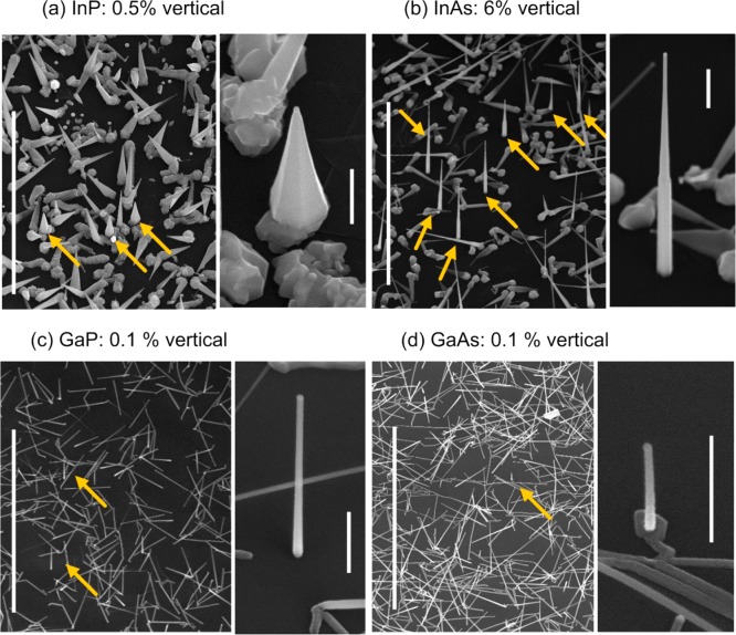
All materials showed a clear, but low, density of vertical NWs (Figure 1). There was no measurable substrate growth, except at the base of nucleated NWs, and the NW growth rates were high as compared to growth on III–V substrates. The group III diffusion lengths are presumably long on the graphite substrate, suggested by the absence of substrate growth. The InAs NWs showed a bottle-like morphology with a thick, straight base and a tapered upper part. Similar InAs NW morphology has been reported from growth on InAs substrates and has been related to surface diffusion.27 Previous reports of InAs NWs on graphene have shown different morphology, probably due to using a different growth mode.28 The nucleation of InAs NWs has been related to graphene layer steps.28 Although we found steps on the graphite substrate, we did not observe higher densities of vertical NWs at these. We also made very limited investigations of InAs NW growth using 30 and 80 nm Au seed particles and saw similar yield as with the 40 nm particles.
Figure 1.
SEM of undoped NWs on graphite: (a) InP, (b) InAs, (c) GaP, and (d) GaAs. Scale bars 10 μm, tilt 30 degrees. Insets show magnifications, scale bars 0.5 μm. Arrows indicate vertical NWs.
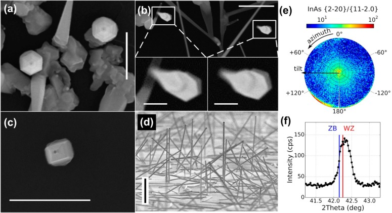
Two samples were analyzed with XRD. We found signal in the center of the pole figure (Figure 2e) for which the radial scan reveals that it corresponds to diffraction from the InAs zincblende (ZB) {2-20} or equivalent wurtzite (WZ) {11-2.0} lattice planes (Figure 2f). The diffraction experiment therefore confirms the presence of crystalline InAs on the sample. Similarly, X-ray diffraction measurements confirmed the presence of crystalline GaP on those samples. III–V NWs often show a mixture of ZB and WZ, and we note that the peak position in Figure 2f fits better to the WZ lattice spacing than to the ZB one.29
Figure 2.
(a) Top view SEM image of two aligned InP NWs. Scale bar 1 μm. (b) Top view SEM image of two InAs NWs, which are rotationally misaligned by about 6°. Scale bar 1 μm. The insets show magnified parts from the same SEM image, scale bars 200 nm. (c) SEM image of InAs NW with rectangular cross-section, scale bar 1 μm. (d) Grazing incidence SEM image of GaP NWs, scale bar 1 μm. (e) X-ray diffraction pole figure and (f) radial scan, of the {2-20} Bragg peak of InAs. The pole figure measurement gives the distribution of ⟨110⟩ direction in a stereographic projection. The center of the plot corresponds to signal from lattice planes parallel to the substrate surface, whereas signal on the outer rim corresponds to lattice planes perpendicular to the substrate.
The facets and the in-plane rotation of the NWs were studied in top-view SEM (Figure 2). Regarding the rotation, Hong et al. found that the side facets of different InAs NWs were aligned,21 while Munshi et al. found either complete alignment or 30 degree rotation of different GaAs NWs.22 In contrast, we found examples of rotationally aligned NWs (Figure 2a), but also some examples of nonaligned NWs (Figure 2b). Most NWs showed 6-fold symmetry of the sidewalls, which is typical for NWs growing in the commonly observed ⟨111⟩B directions. We also observed some InAs NWs with rectangular cross sections (Figure 2c), a morphology that has been observed in InP NWs growing in ⟨001⟩ directions.30
The yield was estimated by inspecting medium-resolution SEM images in randomly selected areas (showing about 500 to 1000 NWs each) and counting the number of vertical NWs and the total number of NWs. Comparing the different materials, we found the highest yield of vertical NWs for InAs (about 6%). InP was significantly worse than InAs with about 0.5% vertical NWs. GaP and GaAs showed a low yield of vertical NWs (about 0.1%). For all materials, there was significant variation over the substrate area with areas of lower and higher density of vertical NWs. In certain areas of about 50 μm2 size, the yield of vertically grown InAs NWs was found to be around 20%. The reason for this variation is unclear. Because of the large variations and low yields, these numbers should merely be seen as rough indications. However, it is clear that the growth of InAs yields a much higher yield of vertical NWs than the other materials. A quantitative yield for self-seeded and SAE NW growth is not easily defined, which prevents a direct comparison with previous reports. Even for GaP, the yield of vertical NWs was too high to be explained by growth in a random orientation. This can be seen in grazing incidence SEM (Figure 2d), where also a few other directions than the vertical one are quite prevalent.
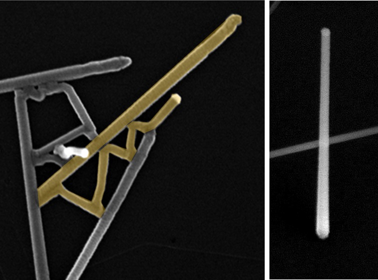
The in-plane NWs were growing in straight but seemingly random directions, which led to seed particles making contact with other NWs. For the In-based materials InAs and InP, this usually led to NWs merging into crystallites. The Ga-based materials GaP and GaAs showed a different and surprising behavior after making contact with other NWs. The seed particles remained intact and were seemingly “reflected” (Figure 3), which created complex patterns of lateral NWs. Such planar NWs have recently attracted increasing scientific interest.31,32 The interfaces between the seed particle and the in-plane GaP NWs were vertical, that is, orthogonal to the growth direction (Figure 3).
Figure 3.
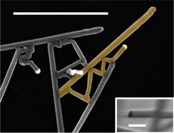
In-plane GaP NW growth. Top view SEM image, scale bar 1 μm. One NW has been false-colored for clarity. The inset shows a grazing incidence SEM image of a NW from the same sample, showing the interface between the seed particle (dark) and the NW. Note that the NW in the inset is not completely orthogonal to the viewing direction, which makes the interface seem slightly tilted.
In situ doping has shown strong effects on NW growth,33,34 for instance, on axial growth rate,35 radial growth,36 crystal structure37 and the interfacial energies at the seed particle–NW interface.37,38 Therefore, we investigated the effects of DEZn, H2S and the in situ etchant HCl on the yield of vertical NWs on graphite with focus on GaP.
No improvements were found with H2S35 or HCl,25 which have previously been shown to affect contact angles and radial growth rates of InP NWs. In contrast, we observed a strong improvement with DEZn (Figure 4). When a high concentration of DEZn (dopant/group III-ratio of molar fraction 1.7) was supplied during NW growth, simultaneously with TMGa and PH3, we observed 1.1% vertical NWs which all curled after about 1 μm length (Figure 4a). This is about 1 order of magnitude better than the reference sample (Figure 1c). Curling has been observed with DEZn-doped InP NWs,38 presumably because the high contact angle induced by Zn makes the seed particle wet the side facets. When the DEZn was supplied 1 min before TMGa (Figure 4b) and in the NW, no straight NWs, vertical nor lateral, were observed. The problem of unstable NW growth was circumvented by switching off the DEZn at the same time as TMGa and PH3 were switched on (Figure 4c). The yield of vertical GaP NWs was about 3.5% with this method and, similar to the results of growing undoped InAs NWs, there were small areas with about 20% yield. With GaAs, we saw a similar improvement with DEZn but not for InAs. The use of DEZn probably affects electronic and structural properties of the III–V NWs39−41 but that issue is outside the scope of this Letter.
Figure 4.
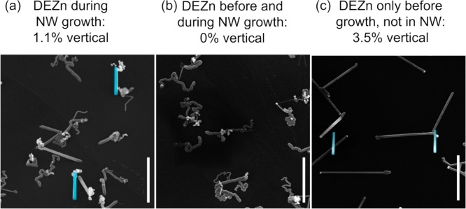
GaP NW growth assisted by DEZn. Scale bars 1 μm, tilt 30°. Vertical NWs have been false-colored in blue.
The overall result from our investigations is that it is possible to grow vertical III–V NWs on graphite irrespective of material but that the yield of vertically grown NWs is quite low or very low. Often NWs were observed after growth to have been growing along the substrate. Note that the NWs that started growing vertically were normally stable and continued in the same direction.
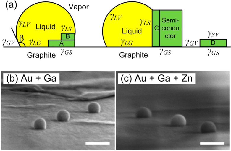
NW growth on graphite and graphene has previously been discussed specifically in terms of lattice matching21,22 but here we use a more general classical nucleation model where lattice matching is indirectly accounted for in the interfacial energies. We consider nucleation and growth at three different positions, as shown in Figure 5a. In a classical nucleation model, there is a reduction in Gibbs free energy by the crystallization from a supersaturated vapor or liquid. The barrier for nucleation is determined by the increase in interfacial energies by forming the crystal. With a smaller relative increase in interfacial energy, the nucleation barrier is lower and the probability higher that the crystal will grow at this position.
Figure 5.
(a) Sketch of metal seed particle (yellow) on graphite substrate, showing possible positions for crystallization (green, lettered A–D). The various interfacial energies, γ, and the contact angle, β, are also shown. (b,c) Grazing incidence SEM of Au nanoparticles on graphite. In (b), TMGa was supplied for 1 min at 500 °C, and in (c) TMGa and DEZn were supplied for 1 min at 500 °C. Scale bars 100 nm.
In order to grow vertical NWs, the desirable growth is in the A position at the interface between the liquid seed particle and the graphite substrate (Figure 5a). However, as soon as a small layer of type A has been grown, it is also possible to nucleate in the B position at the newly formed liquid-semiconductor interface. The ideal scenario for vertical NW growth is that first a complete “A” layer forms after which vertical NW growth can proceed with “B”-type layers. On the other hand, if sufficient layers of type B form it is possible for the NW to grow in-plane with type “C” layers. We assume here that both A and B start at the so-called triple phase boundary (TPB), as is normally the case for VLS growth,42,43 although it is not important for the conclusions. Finally, vapor–solid substrate growth, type D, should be considered.
The A nucleus creates two new interfaces, graphite–semiconductor (γGS) and liquid–semiconductor (γLS), and removes part of the liquid–graphite interface (γLG). The D nucleus instead creates a graphite–semiconductor and a semiconductor–vapor (γSV) interface and removes part of the graphite–vapor interface (γGV). Ignoring the vertical facets, which are small if single layer growth is considered, the changes in interfacial energy per unit area are
| 1A |
| 1B |
| 1C |
| 1D |
Note that classical nucleation theory applied to NW growth often only considers the vertical facets in different variations of “B” nuclei.43
To be able to estimate the relevant interfacial energies, we use Young’s equation at the graphite–liquid–vapor boundary
| 2 |
Here, γGV is very small, about 0.06 J/m2,44 compared with III–Vs, which usually have semiconductor–vapor interfacial energies (γSV) in the range 1 to 2 J/m2.43
To investigate the influence of Zn on the interfacial energies, we annealed Au particles on graphite substrates, providing TMGa with and without DEZn (but no PH3), for 1 min at 500 °C. Although we cannot observe the particles at the growth conditions, the wetting observed after growth (Figure 5b,c) should give an indication of the contact angle. The flatter profile shows that Zn improves the wetting compared with just Ga, although the effect is difficult to quantify. For the annealed particles, we observe contact angles in the order of 120°. That is, cos β ≈ −0.5. The γLV for the metals we have investigated ranges from 0.54 J/m2 (In), 0.72 J/m2 (Ga), 0.79 J/m2 (Zn), to 1.15 J/m2 (Au).45 Assuming γLV = 0.9 J/m2, we can roughly estimate γLG ≈ 0.5 J/m2. This is close to estimated values for γLS.38
The γGS is more difficult to estimate, because it is a solid–solid interface. Molten GaSb46 and GaAs47 show high contact angles (129 to 153°) on graphite, and it was observed that the molten GaSb completely dewets upon freezing.46 Note that GaSb has been predicted to have a relatively good lattice matching with graphene.22 Thus, in this case γGS > γSV = 1.1 J/m2, and we assume similar values for other III–Vs. The high interfacial energy reflects the weak interaction between graphite and III–Vs, which is also manifested in the lack of substrate growth in our experiments.
With these estimates of the interfacial energies, we can use eq 1 to roughly estimate the changes in interfacial energies for the different types of nuclei ΔγA≈ 1 J/m2, ΔγB≈ ΔγC ≈ 0, ΔγD≈ 2 J/m2. Even if these estimates are rough, the large differences allow us to conclude with some certainty that in most cases the following relation holds: ΔγD> ΔγA> ΔγB≈ ΔγC.
Comparing with our experimental results, we note first that ΔγD is the highest, which fits with the observed lack of substrate growth. Previous work has also shown that is difficult to grow a continuous thin film of GaAs on graphite.48 The second conclusion from the estimates of interfacial energies, ΔγA> ΔγC, is also supported by experiments. Most seed particles generate lateral in-plane NWs, rather than vertical NWs. Particularly in the case of GaP, the seed particles crawl on the graphite while the crystal growth proceeds at the vertical liquid–semiconductor interface. Note however that vertical or inclined NW growth is stable once it has started, since the A layer is complete and ΔγB≈ 0. Thus, the unfavorable differences in interfacial energies can explain the overall low yield of vertical NWs.
To increase the vertical NW yield, ΔγA must be reduced, which can be done by decreasing γGS or γLS or by increasing γLG. We observe that Zn strongly improves the vertical NW nucleation for GaP and GaAs. From the annealing experiments, however, we find that Zn reduces the contact angle of Au–Ga particles on graphite, which according to eq 2 suggests that γLG is reduced. At the same time, the curling NW growth at high DEZn concentrations indicates that the contact angle on the NWs increase, consistent with an increased γLS. These findings therefore suggest that Zn should hamper vertical NW growth, which is in stark contrast to our observations.
However, previous experiments of growth of GaAs thin films on graphite have shown strong improvements using Zn.48 Undoped GaAs showed almost spherical crystallites but with in situ doping with Zn a rough thin film was created. Because thin film growth relies on type D nucleation, the improvement with Zn suggests that the key change was a reduction in γGS. From eq 1, we expect that a reduction of γGS would lower both ΔγA and ΔγD. Indeed, inspection of recent reports indicates that a high yield of vertical NW growth on graphene is paired with significant substrate growth.22,23
We can only speculate about the physical mechanism behind a reduced γGS. Munshi et al. discussed the lattice matching between the III–V NW and the graphite substrate,22 and one possibility is that a good lattice matching expresses itself as a low γGS. This could be the case for undoped InAs NWs, which shows by far the highest yield of undoped vertical NWs here. The predicted lattice matching of ZnO to graphite22 could also contribute to the excellent results with this material.19 The addition of dopants, which have different sizes from the host atoms, could allow for a better matching of the III–V lattice to the graphite substrate. The large mismatches, especially of GaAs,22 together with the similar sizes of Ga and Zn atoms, however, makes a size effect an unlikely explanation for the improvement using DEZn. Note also that the reported complete dewetting of frozen GaSb46 occurred despite the excellent lattice matching to graphite.22
An alternative, but not mutually excluding, explanation is based on the strength of the atomic bindings between the semiconductor and graphite. Unlike Ga atoms in GaAs, Zn acceptors in the lattice are charged and may bond with a stronger electrostatic coupling to the carbon atoms in the graphite. A similar explanation was recently proposed for the strong interaction between ZnO and graphite.49
These results suggest that a strategy for improving the yield of vertical NWs is to first seek good growth conditions for thin film growth on graphite. Then, these conditions can be applied to a short nucleation step. Once a layer of semiconductor has grown and the type A layers are complete, the growth conditions can be changed to promote NW growth and suppress substrate growth. Indeed Munshi et al. used a two-step growth sequence, where a 10 s nucleation step, which promoted vertical NW growth but also substrate growth, was followed by NW growth at higher temperature.22 Similarly, we see the best results supplying DEZn before, but not during, GaP NW growth.
In conclusion, we have shown that Au-seeded vertical InP, InAs, GaP, and GaAs NWs can be grown on graphite. While most NWs grow in-plane, the yield of vertical GaP and GaAs NWs could be strongly improved by supplying DEZn before growth. We find that a classical nucleation model can explain the overall low yield of vertical NWs. With further developments, these results pave the way for hybrid graphene–III–V devices, which could take advantage of the unique properties of these two classes of materials.
Methods
Highly ordered pyrolytic graphite (HOPG, grade SPI-2) substrates were obtained from SPI Supplies, Inc. Au nanoparticles (40 nm) were deposited using an aerosol technique,50 which gives Au particles in random positions but with a homogeneous density (1 particle per μm2). The NWs were grown in a low-pressure (100 mbar) metal organic vapor phase epitaxy (MOVPE) system with a total flow of 6 L/min using hydrogen as carrier gas. The precursors were trimethylindium (TMIn), trimethylgallium (TMGa), arsine (AsH3), and phosphine (PH3). The reactor was heated to the growth temperature, and growth was initiated by supplying group III and group V precursors simultaneously. The growth was interrupted by turning off all sources except the group V source and lowering the temperature. High-temperature annealing was normally not used because graphite does not have any surface oxide to desorb, and direct comparisons did not show any difference from such annealing.
The following growth conditions were used:
InAs: Growth temperature, T = 450 °C, χTMI = 7.9 × 10⁻⁶, χAsH3 = 5.5 × 10⁻⁴, growth time t = 5 min.
InP: T = 450 °C, χTMI = 5.1 × 10⁻⁶, χPH3 = 2.5 × 10⁻², t = 10 min.
GaP: T = 475 °C, χTMGa = 1.3 × 10⁻⁵, χPH3 = 2.5 × 10⁻², t = 3 min.
GaAs: T = 450 °C, χTMGa = 1.3 × 10⁻⁵, χAsH3 = 2.2 × 10⁻³, t = 3 min.
For the doped GaP NWs, a DEZn molar fraction of χTMGa = 2.3 × 10⁻⁵ and a growth time of 1 min was used.
XRD pole figure measurements were recorded using Cu Kα radiation in a laboratory diffractometer. Several square millimeters of the sample are illuminated by the X-ray beam, corresponding to a large number of grains of the HOPG substrates. Therefore no in-plane orientation of the nanowires with respect to the substrate lattice can be determined. These pole figure measurements show the orientation of lattice directions for the probed Bragg peaks in the ensemble of nanowires.
Selectivity to the nanowire material is achieved by setting the detector angle to a Bragg angle of the respective material and changing the sample orientation until a diffraction signal from the sample is found. The shown plots represent the stereographic projection of the measured intensity, where the center of the plot corresponds to the surface normal and the outer rim to the directions in the plane of the substrate.
Acknowledgments
This work was performed within the Nanometer Structure Consortium at Lund University (nmC@LU) and was supported by the Swedish Research Council (Vetenskapsrådet), by the Knut and Alice Wallenberg Foundation, by the Swedish Energy Agency, and by the Austrian Science Fund (FWF P23706-N19).
Author Present Address
(J.W.) Institute for X-ray Physics, University of Göttingen Friedrich-Hund-Platz 1, 37077 Göttingen, Germany.
Author Contributions
The manuscript was written through contributions of all authors. All authors have given approval to the final version of the manuscript.
The authors declare no competing financial interest.
References
- Geim A. K.; Novoselov K. S.; Morozov S. V.; Jiang D.; Zhang Y.; Dubonos S. V.; Grigorieva I. V.; Firsov A. A. Electric field effect in atomically thin carbon films. Science 2004, 3065696666–669. [DOI] [PubMed] [Google Scholar]
- Bae S.; Kim H.; Lee Y.; Xu X. F.; Park J. S.; Zheng Y.; Balakrishnan J.; Lei T.; Kim H. R.; Song Y. I.; Kim Y. J.; Kim K. S.; Ozyilmaz B.; Ahn J. H.; Hong B. H.; Iijima S. Roll-to-roll production of 30-in. graphene films for transparent electrodes. Nat. Nanotechnol. 2010, 58574–578. [DOI] [PubMed] [Google Scholar]
- Mazid Munshi A.; Weman H. Advances in semiconductor nanowire growth on graphene. Phys. Status Solidi RRL 2013, 710713–726. [Google Scholar]
- Garnett E. C.; Brongersma M. L.; Cui Y.; McGehee M. D. Nanowire Solar Cells. Annu. Rev. Mater. Res 2011, 41, 269–295. [Google Scholar]
- LaPierre R. R.; Chia A. C. E.; Gibson S. J.; Haapamaki C. M.; Boulanger J.; Yee R.; Kuyanov P.; Zhang J.; Tajik N.; Jewell N.; Rahman K. M. A. III–V nanowire photovoltaics: Review of design for high efficiency. Phys. Status Solidi RRL 2013, 710815–830. [Google Scholar]
- Wallentin J.; Anttu N.; Asoli D.; Huffman M.; Åberg I.; Magnusson M. H.; Siefer G.; Fuss-Kailuweit P.; Dimroth F.; Witzigmann B.; Xu H. Q.; Samuelson L.; Deppert K.; Borgström M. T. InP Nanowire Array Solar Cells Achieving 13.8% Efficiency by Exceeding the Ray Optics Limit. Science 2013, 33961231057–1060. [DOI] [PubMed] [Google Scholar]
- Mariani G.; Scofield A. C.; Hung C.-H.; Huffaker D. L. GaAs nanopillar-array solar cells employing in situ surface passivation. Nat. Commun. 2013, 4, 1497. [DOI] [PMC free article] [PubMed] [Google Scholar]
- Colombo C.; Heibeta M.; Grätzel M. Fontcuberta i Morral, A. Gallium arsenide p-i-n radial structures for photovoltaic applications. Appl. Phys. Lett. 2009, 9417173108–3. [Google Scholar]
- Wernersson L. E.; Thelander C.; Lind E.; Samuelson L. III-V Nanowires-Extending a Narrowing Road. Proc. IEEE 2010, 98122047–2060. [Google Scholar]
- Tomioka K.; Yoshimura M.; Fukui T. A III-V nanowire channel on silicon for high-performance vertical transistors. Nature 2012, 4887410189–192. [DOI] [PubMed] [Google Scholar]
- Thelander C.; Agarwal P.; Brongersma S.; Eymery J.; Feiner L. F.; Forchel A.; Scheffler M.; Riess W.; Ohlsson B. J.; Gösele U.; Samuelson L. Nanowire-based one-dimensional electronics. Mater. Today 2006, 91028–35. [Google Scholar]
- Appenzeller J.; Knoch J.; Björk M. I.; Riel H.; Schmid H.; Riess W. Toward Nanowire Electronics. IEEE Trans. Electron Devices 2008, 55112827–2845. [Google Scholar]
- Duan X. F.; Huang Y.; Cui Y.; Wang J. F.; Lieber C. M. Indium phosphide nanowires as building blocks for nanoscale electronic and optoelectronic devices. Nature 2001, 409681666–69. [DOI] [PubMed] [Google Scholar]
- Minot E. D.; Kelkensberg F.; van Kouwen M.; van Dam J. A.; Kouwenhoven L. P.; Zwiller V.; Borgström M. T.; Wunnicke O.; Verheijen M. A.; Bakkers E. P. A. M. Single quantum dot nanowire LEDs. Nano Lett. 2007, 72367–371. [DOI] [PubMed] [Google Scholar]
- Fortuna S. A.; Wen J.; Chun I. S.; Li X. Planar GaAs Nanowires on GaAs (100) Substrates: Self-Aligned, Nearly Twin-Defect Free, and Transfer-Printable. Nano Lett. 2008, 8124421–4427. [DOI] [PubMed] [Google Scholar]
- Tsivion D.; Schvartzman M.; Popovitz-Biro R.; von Huth P.; Joselevich E. Guided Growth of Millimeter-Long Horizontal Nanowires with Controlled Orientations. Science 2011, 33360451003–1007. [DOI] [PubMed] [Google Scholar]
- Keitaro I.; Fumiya I.; Katsuhiro T.; Takashi F. GaAs nanowire growth on polycrystalline silicon thin films using selective-area MOVPE. Nanotechnology 2013, 2411115304. [DOI] [PubMed] [Google Scholar]
- Lee C. H.; Kim Y. J.; Hong Y. J.; Jeon S. R.; Bae S.; Hong B. H.; Yi G. C. Flexible Inorganic Nanostructure Light-Emitting Diodes Fabricated on Graphene Films. Adv. Mater. 2011, 23, 4614–4619. [DOI] [PubMed] [Google Scholar]
- Hwang J. O.; Lee D. H.; Kim J. Y.; Han T. H.; Kim B. H.; Park M.; No K.; Kim S. O. Vertical ZnO nanowires/graphene hybrids for transparent and flexible field emission. J. Mater. Chem. 2011, 21103432–3437. [Google Scholar]
- Kim Y.-J.; Lee J.-H.; Yi G.-C. Vertically aligned ZnO nanostructures grown on graphene layers. Appl. Phys. Lett. 2009, 9521213101–3. [Google Scholar]
- Park H.; Chang S.; Jean J.; Cheng J. J.; Araujo P. T.; Wang M.; Bawendi M. G.; Dresselhaus M. S.; Bulović V.; Kong J.; Gradečak S. Graphene Cathode-Based ZnO Nanowire Hybrid Solar Cells. Nano Lett. 2012, 131233–239. [DOI] [PubMed] [Google Scholar]
- Hong Y. J.; Fukui T. Controlled van der Waals Heteroepitaxy of InAs Nanowires on Carbon Honeycomb Lattices. ACS Nano 2011, 597576–7584. [DOI] [PubMed] [Google Scholar]
- Munshi A. M.; Dheeraj D. L.; Fauske V. T.; Kim D.-C.; van Helvoort A. T. J.; Fimland B.-O.; Weman H. Vertically Aligned GaAs Nanowires on Graphite and Few-Layer Graphene: Generic Model and Epitaxial Growth. Nano Lett. 2012, 1294570–4576. [DOI] [PubMed] [Google Scholar]
- Katal Mohseni P.; Behnam A.; Wood J. D.; English C.; Lyding J. W.; Pop E.; Li X. In(x)Ga(1-x)As Nanowire Growth on Graphene: van der Waals Epitaxy Induced Phase Segregation. Nano Lett. 2013, 1331153–1161. [DOI] [PubMed] [Google Scholar]
- Mårtensson T.; Borgström M.; Seifert W.; Ohlsson B. J.; Samuelson L. Fabrication of individually seeded nanowire arrays by vapour-liquid-solid growth. Nanotechnology 2003, 14121255–1258. [Google Scholar]
- Borgström M. T.; Wallentin J.; Trägårdh J.; Ramvall P.; Ek M.; Wallenberg L. R.; Samuelson L.; Deppert K. In Situ Etching for Total Control Over Axial and Radial Nanowire Growth. Nano Res. 2010, 34264–270. [Google Scholar]
- Tateno K.; Takagi D.; Zhang G.; Gotoh H.; Hibino H.; Sogawa T. VLS Growth of III-V Semiconductor Nanowires on Graphene Layers. MRS Online Proc. Libr. 2012, 1439, 45–50. [Google Scholar]
- Dayeh S. A.; Yu E. T.; Wang D. Surface Diffusion and Substrate-Nanowire Adatom Exchange in InAs Nanowire Growth. Nano Lett. 2009, 951967–1972. [DOI] [PubMed] [Google Scholar]
- Hong Y. J.; Lee W. H.; Wu Y.; Ruoff R. S.; Fukui T. van der Waals Epitaxy of InAs Nanowires Vertically Aligned on Single-Layer Graphene. Nano Lett. 2012, 1231431–1436. [DOI] [PubMed] [Google Scholar]
- Kriegner D.; Panse C.; Mandl B.; Dick K. A.; Keplinger M.; Persson J. M.; Caroff P.; Ercolani D.; Sorba L.; Bechstedt F.; Stangl J.; Bauer G. Unit Cell Structure of Crystal Polytypes in InAs and InSb Nanowires. Nano Lett. 2011, 1141483–1489. [DOI] [PubMed] [Google Scholar]
- Krishnamachari U.; Borgstrom M.; Ohlsson B. J.; Panev N.; Samuelson L.; Seifert W.; Larsson M. W.; Wallenberg L. R. Defect-free InP nanowires grown in [001] direction on InP(001). Appl. Phys. Lett. 2004, 85112077–2079. [Google Scholar]
- Givargizov E. I. Periodic Instability in Whisker Growth. J. Cryst. Growth 1973, 203217–226. [Google Scholar]
- Wallentin J.; Borgström M. T. Doping of semiconductor nanowires. J. Mater. Res. 2011, 26172142–2156. [Google Scholar]
- Wallentin J.; Mergenthaler K.; Ek M.; Wallenberg L. R.; Samuelson L.; Deppert K.; Pistol M. E.; Borgström M. T. Probing the Wurtzite Conduction Band Structure Using State Filling in Highly Doped InP Nanowires. Nano Lett. 2011, 1162286–2290. [DOI] [PubMed] [Google Scholar]
- Lauhon L. J.; Gudiksen M. S.; Wang C. L.; Lieber C. M. Epitaxial core-shell and core-multishell nanowire heterostructures. Nature 2002, 420691157–61. [DOI] [PubMed] [Google Scholar]
- Algra R. E.; Verheijen M. A.; Borgström M. T.; Feiner L.-F.; Immink G.; van Enckevort W. J. P.; Vlieg E.; Bakkers E. P. A. M. Twinning superlattices in indium phosphide nanowires. Nature 2008, 4567220369–372. [DOI] [PubMed] [Google Scholar]
- Wallentin J.; Ek M.; Wallenberg L. R.; Samuelson L.; Deppert K.; Borgström M. T. Changes in Contact Angle of Seed Particle Correlated with Increased Zincblende Formation in Doped InP Nanowires. Nano Lett. 2010, 10124807–4812. [DOI] [PubMed] [Google Scholar]
- Gutsche C.; Regolin I.; Blekker K.; Lysov A.; Prost W.; Tegude F. J. Controllable p-type doping of GaAs nanowires during vapor-liquid-solid growth. J. Appl. Phys. 2009, 1052024305. [Google Scholar]
- Novak J.; Šoltýs J.; Eliáš P.; Hasenöhrl S.; Stoklas R.; Dujavová A.; Mikulics M. Electrical properties of individual GaP nanowires doped by zinc. Phys. Status Solidi a 2012, 209122505–2509. [Google Scholar]
- Algra R. E.; Verheijen M. A.; Feiner L.-F.; Immink G. G. W.; Enckevort W. J. P. v.; Vlieg E.; Bakkers E. P. A. M. The Role of Surface Energies and Chemical Potential during Nanowire Growth. Nano Lett. 2011, 1131259–1264. [DOI] [PubMed] [Google Scholar]
- Wacaser B. A.; Dick K. A.; Johansson J.; Borgström M. T.; Deppert K.; Samuelson L. Preferential Interface Nucleation: An Expansion of the VLS Growth Mechanism for Nanowires. Adv. Mater. 2009, 212153–165. [Google Scholar]
- Dubrovskii V. G.; Sibirev N. V.; Harmand J. C.; Glas F. Growth kinetics and crystal structure of semiconductor nanowires. Phys. Rev. B 2008, 7823235301. [Google Scholar]
- Wang S.; Zhang Y.; Abidi N.; Cabrales L. Wettability and Surface Free Energy of Graphene Films. Langmuir 2009, 251811078–11081. [DOI] [PubMed] [Google Scholar]
- Mills K. C.; Su Y. C. Review of surface tension data for metallic elements and alloys: Part 1 - Pure metals. Int. Mater. Rev. 2006, 516329–351. [Google Scholar]
- Harter I.; Dusserre P.; Duffar T.; Nabot J. P.; Eustathopoulos N. Wetting of III–V melts on crucible materials. J. Cryst. Growth 1993, 1311–2157–164. [Google Scholar]
- König U.; Keck W. Contact Angles Between III–V Melts and Several Substrates. J. Electrochem. Soc. 1983, 1303685–686. [Google Scholar]
- Johnston W. D.; Callahan W. M. Properties of Polycrystalline AlAs/GaAs on Graphite Heterojunctions for Solar Cell Applications. J. Electrochem. Soc. 1978, 1256977–983. [Google Scholar]
- Galan U.; Sodano H. A. Molecular dynamics prediction of interfacial strength and validation through atomic force microscopy. Appl. Phys. Lett. 2012, 10115151603–4. [Google Scholar]
- Magnusson M. H.; Deppert K.; Malm J. O.; Bovin J. O.; Samuelson L. Size-selected gold nanoparticles by aerosol technology. Nanostruct. Mater. 1999, 121–445–48. [Google Scholar]


