

Significance
It is widely believed that surface area-to-volume ratio is directly related to the sensitivity of field-effect transistor-based biosensors; this has led to a massive drive to use nanowires, which are costly and difficult to make, for use in such sensors. Although nanowires do exhibit superior performance in certain situations, we believe increased surface area-to-volume ratio is not the cause. We find that in general, smaller wires do worse, unless they are placed on an insulating substrate. In the corners between the nanowire and the substrate, the electrolyte exhibits weaker Debye screening and smaller capacitance density, causing the sensor to have larger charge sensitivity. Our understanding enables researchers to design better biosensors, possibly using large-scale structures that are cheaper to make.
Keywords: nanowire, Debye screening, scaling, bioFET, electric-double-layer
Abstract
Electrostatic counter ion screening is a phenomenon that is detrimental to the sensitivity of charge detection in electrolytic environments, such as in field-effect transistor-based biosensors. Using simple analytical arguments, we show that electrostatic screening is weaker in the vicinity of concave curved surfaces, and stronger in the vicinity of convex surfaces. We use this insight to show, using numerical simulations, that the enhanced sensitivity observed in nanoscale biosensors is due to binding of biomolecules in concave corners where screening is reduced. We show that the traditional argument, that increased surface area-to-volume ratio for nanoscale sensors is responsible for their increased sensitivity, is incorrect.
In recent years, there has been a major drive to use field-effect transistor (FET)-based devices to detect biological molecules in electrolytic environments (1). These biosensors use the charge of biomolecules to gate the current through a transistor (2). Frequently, the transistor is based on a quasi-1D nanostructure, such as a nanowire (NW) or nanotube, and the biomolecules bind directly to the surface of the nanoscale structure (1, 3). The use of such nanostructures is justified by the belief that nanoscale biosensors are more sensitive, with sensitivity defined as the relative change in drain current or a shift in threshold voltage in response to a change in bound biomolecule density. A few experiments specifically studied the effect of shrinking nanowire radii on sensitivity, albeit with varying structures, analytes, and sensing circumstances, and found that shrinking a sensor’s dimensions indeed improves its sensitivity (4–6). The enhanced sensitivity has been loosely attributed to the increase in the sensor’s surface area-to-volume ratio, which is a direct result of shrinking its dimensions. This argument has been analytically justified in the context of gas sensors (7). However, there is a fundamental difference between gas and biomolecule sensing: biomolecule sensing is performed in an electrolyte, and the ions therein will screen the charge of bound biomolecules in a phenomenon known as Debye screening (8, 9). The direct application of the gas sensing result to the biosensing environment implicitly assumes that the screening effect does not change with shrinking dimensions, an assumption we believe to be false. There have been studies that included a rigorous treatment of screening in biosensors, but they studied neither the specific cause of increased sensitivity at the nanoscale, nor the effect of varying size on screening behavior (10). We believe the phenomenon responsible for the increased sensitivity of nanowires in particular, and nanostructured biosensors in general, have not yet been uncovered by the research community.
We have previously dissected the operation of biosensors into two independent parts to better understand the underlying physics (11): first, biomolecule charges cause a change in the local electrostatic potential at the outer surface of the gate dielectric. This potential change in turn causes a change in the drain current of the underlying semiconductor channel. The latter part is simply the transconductance effect of an FET-based transistor; nanoscale biosensors have no advantage in this respect over planar sensors. The nanoscale advantage should therefore lie in the first part of the sensor operation, which is a capacitive transduction effect, dominated by the capacitance of the Debye screening layer. We therefore believe understanding screening behavior at the nanoscale is key to understanding the behavior of nanoscale biosensors.
In this paper, we revisit screening near curved nanostructure surfaces by solving the Poisson–Boltzmann equation that led to the original Debye–Hückel formalism. Our simple analytical arguments will show that screening is stronger near surfaces with convex curvature, and weaker near surfaces with concave curvature. We only consider simple convex and concave surfaces because almost all nonplanar surfaces can be decomposed into local areas with either convex or concave curvature.
Next, we apply the basic insight we gain from the previous step to understand and analyze the specific case of nanowire biosensors. Increasing the surface area-to-volume ratio of nanowire sensors actually means increasing their convexity, which should result in increased Debye screening and reduced sensitivity. However, nanowires placed on insulating substrates create concave corners between the nanowire and the substrate. We believe biomolecules bound in such concave corners are responsible for the increased sensitivity experimentally observed in nanowires.
Methods
Analytical Calculations.
We begin by noting that biosensor sensitivity has been shown to be maximum when the biosensor is operated in the subthreshold regime (11, 12). In this regime, sensitivity can be defined as either a change in effective gate potential (or threshold voltage) or a relative change in drain current. These definitions are proportional to one another, as shown below. We will therefore treat them as equivalent for the purposes of assessing the effects of nanowire radius on sensitivity.
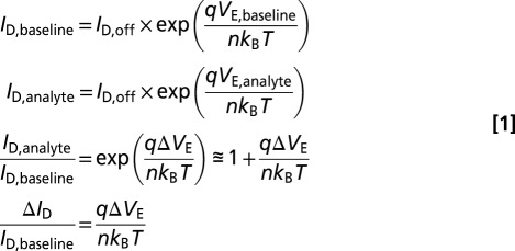 |
In the above expressions,  ,
,  , and
, and  represent the drain current in the off-state, the baseline drain current in the absence of target analytes, and the drain current in the presence of target analytes, respectively. Variables n, q, kB, and T represent the subthreshold ideality factor, elementary charge, Boltzmann’s constant, and temperature, respectively. VE denotes the electrode potential in extended-gate biosensors, which corresponds to the potential at the electrolyte/oxide interface for nanowire FET biosensors; this potential acts upon a biosensor’s channel as the gate voltage would in a regular FET.
  and
and  represent the change in drain current and electrode potential due to target biomolecule binding. We have assumed that the target analyte concentration is small, resulting in
 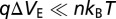 .
.
In a previous paper (11), we dissected a generic FET-based biosensor’s response into four parts, as follows:
 |
Here,  is the change in target analyte concentration and
  is the change in surface charge density due to the target analytes; these are unaffected by geometry. The third term in the equation above represents capacitive transduction, whose geometry dependence is dealt with elsewhere in this paper. The final term captures the transistor action of a biosensor. This term is none other than the familiar
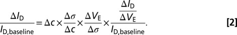
  of a transistor, which is largest when the FET is operated in the subthreshold regime, and is the main reason why sensitivity is maximum under subthreshold operation. However, it should be noted that in subthreshold,
  has a theoretical maximum:
 |
The above maximum for  is simply the familiar 60-mV per decade limitation for the subthreshold swing of thermionic FETs. Reducing nanowire diameter will improve sensitivity by improving
  . However, once the fundamental maximum has been reached, further reduction in size does not provide any improvement. Biosensing nanowires are typically doped at ∼
 , for which the maximum depletion width is ∼300 nm at room temperature; this is far larger than the typical dimensions of the nanowires, most of which are thinner than 100 nm. Nanowires used in most biosensing experiments are therefore already fully depleted, and further reduction in size will not noticeably change or improve subthreshold swing. Once a nanowire is fully depleted, changing its radius will only change the third term in Eq. 2, which represents the capacitive transduction of biomolecule charge into surface potential at the electrolyte/oxide interface. We can therefore safely ignore the FET action of the nanowire, and focus our analysis on the capacitive term and its variations due to surface curvature. It should be noted that most nanowires do not exhibit the 60-mV per decade ideal swing, even though they are fully depleted; this is due to the large number of interface trap states created during processing.
To describe sensing near generic curved surfaces, it is sufficient to solve the Poisson–Boltzmann equation, subject to the proper boundary conditions; this method is known as the Gouy–Chapman model (8). This model neglects the finite size of the ions in the electrolyte. It is adequate for gaining insight into the qualitative behavior of electric double layers; for low surface potentials and dilute electrolytes, it is also quantitatively acceptable (13). Calculations using more sophisticated modified Poisson–Boltzmann formalisms have arrived at potential distributions similar to ours (14).
To make the problem analytically tractable, we solve the equation in 1D, and extend it to 3D using cylindrical and spherical symmetries. We consider five different types of structures: (i) flat, (ii) convex spherical, similar to a nanoparticle, (iii) convex cylindrical, similar to a nanowire, (iv) concave spherical, similar to a cavity in an otherwise solid electrode, and (v) concave cylindrical, similar to a cylindrical pore through an electrode, such as those used in nanopore translocation sensing. We vary the radii of curvature in the curved structures, and extract sensitivity as a function of radius. Cross-sections of concave, flat, and convex structures are shown in Fig. 1, respectively; the cross-sections of concave cylindrical and spherical structures look identical, as do their convex counterparts.
Fig. 1.

Cross-sectional schematics of the structures that were analytically studied. The concave, flat, and convex structures are shown in A, B, and C, respectively; the cross-sections of concave cylindrical and spherical structures look identical, as do their convex counterparts. The gold areas represent the sensing electrode, the teal areas represent the electrolyte, and the dotted red lines represent the charged target biomolecules.
All structures are composed of a 1:1 electrolyte in contact with a polarizable sensing electrode. A grounded reference electrode immersed in the electrolyte is modeled by fixing the electrolyte Fermi level at 0 V. For the convex and flat cases, the electrostatic potential from the sensing electrode is required to vanish far away from the electrode surface. For the concave cases, the electric field is required to vanish at the center of the structure, due to symmetry.
For the next steps, we refer the reader to Fig. 2. We solve Poisson’s equation, find the electrostatic potential in the electrolyte in terms of the electrode potential VE, and find the total ionic charge in the electrolyte as a function of the VE. The derivative of this charge with respect to VE gives the capacitance density of the diffuse ionic layer, denoted by CDL. The calculation is straightforward, and the details are given in the accompanying Supporting Information.
Fig. 2.

Schematic depiction of the potential diagram across a generic nanowire biosensor, as well as the capacitive divider that is seen by the biomolecules. This generic diagram applies to all structures of interest. CDL, COX, and CNW represent the capacitances due to the diffuse layer in the electrolyte, the gate dielectric, and the mobile carriers in the nanowire, respectively. The blue and red potential diagrams correspond to the prebinding and postbinding states of the sensor; i.e., the blue diagram has only charged receptors at the oxide surface, whereas the red curve has both charged receptors and charged analytes. The analytes cause a potential change  at the outer surface of the gate dielectric, which we consider to be the sensor’s sensitivity. The potential change is screened, and decays with distance into the nanowire and electrolyte regions.
The charges brought by biomolecules to the electrode surface are modeled as a uniform layer of sheet charge of density  ; these can be viewed as a small-signal disturbance, with the sensing and reference electrodes representing small-signal ground. The capacitance between the biomolecule charges and ground is therefore the parallel combination of the diffuse layer capacitance, CDL, and the capacitance to the sensing electrode, CE. The justification for such an equivalent circuit model is given in Supporting Information. The local potential change near the biomolecules is determined by the following equation:
In a real system such as a nanowire FET-based biosensor, CE includes the “gate” dielectric capacitance between the FET and the electrolyte, COX, in series with the semiconductor capacitance of the underlying FET, CNW. If the FET part of the sensor is made of silicon, and is operated in the subthreshold regime as recommended (11, 12), the Debye length in the FET channel will be on the order of 40 μm, and the relative permittivity will be 11.7. The gate dielectric capacitance can be neglected when in series with the much smaller semiconductor capacitance. In stark contrast, the Debye length in the electrolyte, assuming physiological ionic strength, will be on the order of 1 nm, with a relative permittivity of 80. The electrolyte capacitance CDL is therefore almost always dominant, allowing us to forego calculating the potential and capacitance of the sensor itself. At this point, the only meaningful dependence of a nanowire biosensor’s sensitivity on its radius is through changes in electrolyte screening, i.e., the capacitance of the diffuse ionic layer, CDL.
Numerical Calculations.
Taking advantage of symmetry allows simple structures to be reduced to 1D and solved analytically. However, for more complex geometries, the analytical calculation becomes intractable. We therefore used a numerical simulator (15) to solve Poisson’s equation. The use of this simulator has the added benefit of solving drift-diffusion equations in the semiconductor regions, allowing us to directly extract drain currents, threshold voltages, and sensitivities.
We simulate two types of 3D nanowires: (i) suspended in solution [suspended nanowire (SNW)], and (ii) placed on an insulating substrate [nanowire-on-insulator (NWoI)]. The former is not commonly encountered in real biosensor systems, whereas the latter is very common. We also consider two cases of biomolecule binding: uniform functionalization (UF), where biomolecules bind to all dielectric surfaces, and selective functionalization (SF), where biomolecules bind only to the outer surfaces of the nanowires’ gate dielectrics (16). Overall the three structures depicted in Fig. 3 A–C are considered: (i) UF–SNW, (ii) UF–NWoI, and (iii) SF–NWoI. The lack of a dielectric substrate makes selective functionalization meaningless for suspended nanowires. We vary the nanowire width in these structures and study the sensitivity behavior.
Fig. 3.
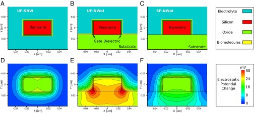
Two-dimensional cross-sectional plots of the simulation structures (A–C) and simulation results of the change in electrostatic potential due to the charge of the biomolecules, taken across the center of the channel (D–F). Structures A and D depict the suspended nanowire case (UF–SNW) surrounded by electrolyte; B and E depict the NWoI case with biomolecules at all dielectric/electrolyte interfaces (UF–NWoI); and C and F depict the selectively functionalized NWoI case with biomolecules on the gate dielectric/electrolyte interface only (SF–NWoI). Note how the potential change is larger near the concave corners, and smaller near convex corners. The lower (concave) corners in F behave like a flat surface (for screening purposes), because there are charges only on the nanowire side of the corner. The yellow biomolecule layers in A–C are artificially added for clarity to denote the locations where biomolecules are present; the simulated biomolecules have no thickness.
The nanowires are presumed to be silicon, covered by a thin dielectric; the outer surface of the gate dielectric is exposed to the electrolyte. The biomolecules were modeled as a sheet charge of uniform density of  at the electrolyte/dielectric interface. Although in reality the molecules are discrete, the random nature of their binding will, on average, resemble a uniform layer of charge. The justification for our choice of biomolecule model is given in Supporting Information. The biomolecule density and electrode potentials were chosen to ensure that the sensor surface potential remained low enough to justify neglecting the finite size of the ions (13), and high enough to ensure accuracy in the presence of quantization errors. Further details of the simulation structure are given in Supporting Information. The sensitivity, in the form of threshold voltage change
  , which is proportional to
  , is extracted and plotted as a function of nanowire radius for our different structure types.
Results
Analytical Results.
First, we look at the electrostatic potential in the electrolyte as a function of distance from various simple surfaces, shown in Fig. 4. The electrostatic potential is normalized to the electrode potential VE. The distances are normalized to the Debye length λ. All of the curved surfaces in this figure have the same radius, equal to five Debye lengths. Note that this figure serves merely to compare the strength of screening near various surface geometries for a given electrode potential; in real biosensors, the electrode potential is measured, not fixed.
Fig. 4.

Plot of electrostatic potential in the electrolyte vs. distance from the surface of the electrodes. The distance is normalized to the Debye length λ, and the potential is normalized to the electrode potential VE. The radius of curvature of the curved surfaces is  .
.
The diffuse layer capacitances for the various geometries that were analyzed are given in Table 1 as a function of the radius of curvature. Here, I and K denote the modified Bessel functions of the first and second kinds, respectively; λ denotes the Debye length in the electrolyte, ϵ denotes the permittivity of the electrolyte, R is the radius of curvature, and  is a dimensionless radius variable. The capacitance densities, normalized to that of the flat case, are plotted in Fig. 5 as a function of the dimensionless radius variable x.
Table 1.
Capacitance of the diffuse layer near electrode with various geometries
| Structure | Screening capacitance |
| Convex spherical |  |
| Convex cylindrical |  |
| Flat |  |
| Concave cylindrical |  |
| Concave spherical | 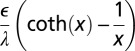 |
Fig. 5.

Plot of electrolyte capacitance density vs. radius of curvature of electrode. The radius is normalized to the Debye length λ, and the capacitances are normalized to that of the flat electrode. Note that the vertical axis is on a logarithmic scale.
Simulation Results.
The simulations offer two sets of results. The first is a set of 2D cross-sectional plots of the change in electrostatic potential due to the charge of the biomolecules, taken across the center of the channel; these are shown in Fig. 3 D–F, for the three structure types, UF–SNW, UF–NWoI, and SF–NWoI, respectively. Contour lines are provided as a visual guide. Note how the potential change is smaller near convex corners, i.e., all of the corners of the UF-SNW structure, and the top corners of both NWoI structures. Conversely, the potential change is larger near the concave corners, i.e., the bottom corners of the UF-NWoI structure. It is important to note that the bottom corners of the SF-NWoI structure do not behave like corners at all, because there are no biomolecules on the substrate, so there is no screening contribution from the substrate facets of these corners.
The second set of results is shown in Fig. 6 as a plot of the sensitivity vs. nanowire width for all three structure types.
Fig. 6.

Plot of the simulated sensitivity vs. nanowire width for the UF–SNW (blue line with square markers), UF–NWoI (green line with diamond markers), and SF–NWoI (red line with circular markers). The sensitivity of the UF–NWoI improves with shrinking width, but those of the UF–SNW and SF–NWoI degrade. The sensitivities of all structures converge to the same value at large widths.
Discussion
We begin our discussion with the analytical results in Fig. 4. This plot shows that the electrostatic potential drops more quickly to its bulk value when the surfaces are convex, and more gradually when the surfaces are concave. Both effects are more drastic for the spherical curvatures. A similar result was obtained by Dickinson and Compton (17) for hemispherical electrodes in the context of electrochemistry. This trend is a direct indicator of screening strength: concave surfaces experience less screening than a flat surface, whereas convex surfaces see more screening. It seems that the more the electrolyte surrounds the surface, the stronger the screening will be. Conversely, the more the surface surrounds the electrolyte, the weaker the screening will be.
Next, we calculated the capacitance due to the electrolyte, and from that, the sensitivity of the electrolyte to biomolecule charges. The results are plotted in Fig. 5 as a function of the radius of curvature of the surface. The increased screening near the convex structures is seen once again, this time in the form of increased capacitance, and over all radii. Similarly, concave structures always exhibit lower screening. Unsurprisingly, the effect is once again more drastic for the spherical surfaces. The potential change is intimately and inversely related to the capacitance, so concave surfaces exhibit higher sensitivity than convex surfaces over all radii.
Intuitively, this trend can be explained as follows: a convex curvature will allow a larger volume of solution to approach the surface, carrying with it more ions, leading to more screening. The opposite happens for the concave curvature. Moreover, a convex spherical surface allows more solution ions to approach a unit of surface area than a convex cylindrical surface, explaining the increased screening for the spherical convex case. A similar argument can be made for the spherical concave case.
We can extend our intuition further by loosely defining a Debye volume as the volume of electrolyte within one Debye length of a surface, similar to a Debye sphere in plasma physics (18). This concept is depicted in Fig. 7, where we have two electrodes with cylindrical surfaces: one convex (similar to a nanowire) and one concave (similar to a pore). For clarity, we omit the bulk of the electrolyte environment from the drawing, and consider the Debye volume for only a fraction of the electrode surfaces. Due to the direction of the curvature, a patch of the surface of the concave electrode has a larger Debye volume than an equally sized patch on the convex electrode, even though the Debye lengths are the same. Because this Debye volume is filled with counter ions, it makes intuitive sense that the convex surface will have more counter ions near it than the concave surface, and consequently will have stronger screening as well. To roughly compare the screening strength near surfaces with arbitrary geometry, we can compare the surface area-to-Debye-volume ratio: the smaller it is, the stronger the screening will be. Of course, there is no rigorous quantitative use for such a quantity; it is only an intuitive guide to help us design electrode structures with appropriate screening. For biosensing purposes, we should seek to increase the surface area-to-Debye-volume ratio of electrodes. In nanoscale sensors where the semiconductor region shares a surface with the electrolyte, downscaling dimensions and increasing the surface area-to-volume ratio are inevitably accompanied by reduced surface area-to-Debye-volume ratio, and hence increased screening and reduced sensitivity.
Fig. 7.

A sketch of the imaginary Debye volume of two electrodes. (Left) Convex electrode. (Right) The pore of this structure is a concave electrode. The electrolyte environment has been omitted for clarity. The Debye volumes are part of the electrolyte environment, and are sketched here for one-quarter of the electrode surfaces. The radii of curvature are equal, and so the surface areas under consideration are equal as well (marked with black curved double-sided arrows). The Debye length is marked with a straight double-sided arrow. Although the Debye lengths and surface areas under consideration are equal, the Debye volume belonging to the convex surface (Debye vol. 1) is larger than that of the concave surface (Debye vol. 2). The variation in Debye volume depends on the relative size of the radius of curvature compared with the Debye length. The Debye volume is correlated with the screening strength, which is stronger near the convex surface relative to the concave surface. By qualitatively evaluating the Debye volume of arbitrary surfaces, one can get a rough idea of the relative screening strength near those surfaces.
The simulation results convey the same idea. In all cases, the charge density is constant, so the potential change in Fig. 3 is a direct indicator of screening strength. In the UF-SNW structure, the corners can be viewed as extremely small areas of extreme convexity; this results in increased screening and smaller potential change, which is directly apparent in the figure. Conversely, in the UF-NWoI structure, the corner between the NW and substrate is concave, giving rise to reduced screening and increased potential change. In the SF-NWoI structure, there are no charges on the substrate, so the lower corners have charges only on one of their sides. The contour lines are nearly parallel to the vertical side of the NW, indicating that the screening is similar to screening near a flat vertical surface; this indicates that the substrate side merely serves as an end to what otherwise behaves like a flat vertical surface.
In all structures, as the NW width is varied, the size of the corner regions remains unchanged. As the nanowires become wider, these corners constitute a smaller fraction of the total sensor surface, and their effect diminishes; eventually, all three structures begin to resemble a flat electrode, seen in the plots of sensitivity vs. width in Fig. 6, where all three curves converge to the same value for large widths. Conversely, as the width shrinks, the relative importance of the corner effect increases. The sensitivity of the UF–SNW structure decreases, because this structure has four convex corners. The SF–NWoI structure has two convex corners and two neutral, so its sensitivity fares better than that of the UF–SNW structure. The UF–NWoI structure has two concave corners whose effect apparently dominates the convex corners, resulting in increased sensitivity with reduced width.
It is worth noting that the sensitivity of the UF-SNW structure decreases with shrinking width, even though its conventional surface area-to-volume ratio increases; this indicates that contrary to conventional wisdom, increased surface area-to-volume ratio does not cause enhanced sensitivity in nanowires.
Although we have only varied width in this study, similar results are expected for varying thickness: for a structure with more overall convexity, reducing surface area harms sensitivity and should be avoided; conversely, if the structure has more overall concavity, reducing the total surface area will increase sensitivity. The latter case applies to nanowires, so long as biomolecules can bind to the substrate as well.
There is an alternative way to analyze the results above, as follows: of all of the biomolecules that bind to the substrate, the few who are within a certain distance of the nanowire are capable of influencing it. The quantity of these biomolecules is independent of the nanowire size; they provide an extra boost to the sensitivity in addition to the biomolecules that bind directly to the nanowire. As the nanowire shrinks, the relative importance of the substrate-bound biomolecules increases, increasing the overall sensitivity.
Conclusions
Although the Gouy–Chapman model is over a century old, the results of its application to nonplanar structures is not well known in the biosensor community. The conclusion is rather simple: screening is weaker near concave surfaces, and stronger near convex surfaces. We believe understanding the effects of curvature on Debye screening enables us to design better electrode surfaces. Although such optimizations have not been discussed here, the surface area-to-Debye-volume ratio is a concept that could be of use in such optimization efforts. We hope the insight gained here will be useful for other sensor systems in which electrostatics are important, such as FET-based sequencing technologies (19) or nanopore sensors (20).
Our analysis has also enabled us to determine that increased surface area-to-volume ratio is not responsible for the sensitivity enhancement that accompanies quasi-1D nanoscale biosensor structures. Instead, it is the overall concavity of the structure, and the binding of biomolecules in concave areas, which results in higher sensitivity. This finding has important implications for the future of biosensors: efforts are underway to increase the limit of detection of biosensors by ensuring that biomolecules bind only to the NW directly (16, 21). However, the conventional wisdom—that nanoscale structures are more sensitive—fails in this regime. It should be noted, however, that our crude modeling of the biomolecules as a uniform sheet of charge neglects many factors that become important when one seeks to detect samples with very low concentrations of analytes. Further studies should include the intricacies of ion and biomolecule size, and the finite supply of biomolecules when analyte concentrations are near the limit of detection.
Supplementary Material
Acknowledgments
The authors thank Mr. Andrew Pan for devoting his time to discussions that helped crystallize the ideas in this paper. Support for this work was provided by National Science Foundation Grant 1128673.
Footnotes
The authors declare no conflict of interest.
This article is a PNAS Direct Submission. M.B. is a guest editor invited by the Editorial Board.
This article contains supporting information online at www.pnas.org/lookup/suppl/doi:10.1073/pnas.1315485111/-/DCSupplemental.
References
- 1.Wang J. Electrochemical biosensors: Towards point-of-care cancer diagnostics. Biosens Bioelectron. 2006;21(10):1887–1892. doi: 10.1016/j.bios.2005.10.027. [DOI] [PubMed] [Google Scholar]
- 2.Gotoh M, Suzuki M, Kubo I, Tamiya E, Karube I. Immuno-FET sensor. J Mol Catal. 1989;53(3):285–292. [Google Scholar]
- 3.Jacobs CB, Peairs MJ, Venton BJ. Review: Carbon nanotube based electrochemical sensors for biomolecules. Anal Chim Acta. 2010;662(2):105–127. doi: 10.1016/j.aca.2010.01.009. [DOI] [PubMed] [Google Scholar]
- 4.Elfström N, et al. Surface charge sensitivity of silicon nanowires: Size dependence. Nano Lett. 2007;7(9):2608–2612. doi: 10.1021/nl0709017. [DOI] [PubMed] [Google Scholar]
- 5.Li J, Zhang Y, To S, You L, Sun Y. Effect of nanowire number, diameter, and doping density on nano-FET biosensor sensitivity. ACS Nano. 2011;5(8):6661–6668. doi: 10.1021/nn202182p. [DOI] [PubMed] [Google Scholar]
- 6.Stern E, et al. Label-free immunodetection with CMOS-compatible semiconducting nanowires. Nature. 2007;445(7127):519–522. doi: 10.1038/nature05498. [DOI] [PubMed] [Google Scholar]
- 7.Fan Z, Lu J. Chemical sensing with ZnO nanowire field-effect transistor. IEEE Trans Nanotechnol. 2006;5(4):393–396. [Google Scholar]
- 8.Bard AJ, Faulkner LR. Electrochemical Methods: Fundamentals and Applications. New York: Wiley; 2001. [Google Scholar]
- 9.McLaughlin S. Electrostatic potentials at membrane-solution interfaces. Curr Top Membr Transp. 1977;9:71–144. [Google Scholar]
- 10.Sørensen MH, Mortensen NA, Brandbyge M. Screening model for nanowire surface-charge sensors in liquid. Appl Phys Lett. 2007;91(10):102105. [Google Scholar]
- 11.Shoorideh K, Chui CO. Optimization of the sensitivity of FET-Based biosensors via biasing and surface charge engineering. IEEE Trans Elect Dev. 2012;59(11):3104–3110. [Google Scholar]
- 12.Gao XPA, Zheng G, Lieber CM. Subthreshold regime has the optimal sensitivity for nanowire FET biosensors. Nano Lett. 2010;10(2):547–552. doi: 10.1021/nl9034219. [DOI] [PMC free article] [PubMed] [Google Scholar]
- 13.Torrie GM, Valleau JP. Electrical double layers. I. Monte Carlo study of a uniformly charged surface. J Chem Phys. 1980;73:5807–5816. [Google Scholar]
- 14.Wang H, Pilon L. Accurate simulations of electric double layer capacitance of ultramicroelectrodes. J Phys Chem Comm. 2011;115(33):16711–16719. [Google Scholar]
- 15. Synopsys (2011) TCAD Sentaurus Suite, version F-2011.09 (Synopsys, Research Triangle Park, NC)
- 16.Park I, Li Z, Pisano AP, Williams RS. Selective surface functionalization of silicon nanowires via nanoscale joule heating. Nano Lett. 2007;7(10):3106–3111. doi: 10.1021/nl071637k. [DOI] [PubMed] [Google Scholar]
- 17.Dickinson EJF, Compton RG. Diffuse double layer at nanoelectrodes. J Phys Chem C. 2009;113(41):17585–17589. [Google Scholar]
- 18.Jackson JD. Classical Electrodynamics. New York: Wiley; 1975. [Google Scholar]
- 19.Rothberg JM, et al. An integrated semiconductor device enabling non-optical genome sequencing. Nature. 2011;475(7356):348–352. doi: 10.1038/nature10242. [DOI] [PubMed] [Google Scholar]
- 20.Reiner JE, et al. Disease detection and management via single nanopore-based sensors. Chem Rev. 2012;112(12):6431–6451. doi: 10.1021/cr300381m. [DOI] [PubMed] [Google Scholar]
- 21.Kim JY, et al. Surface engineering for enhancement of sensitivity in an underlap-FET biosensor by control of wettability. Biosens Bioelectron. 2013;41:867–870. doi: 10.1016/j.bios.2012.08.036. [DOI] [PubMed] [Google Scholar]
Associated Data
This section collects any data citations, data availability statements, or supplementary materials included in this article.