Abstract
Localization of large electric fields in plasmonic nanostructures enables various processes such as single molecule detection, higher harmonic light generation, and control of molecular fluorescence and absorption. High-throughput, simple nanofabrication techniques are essential for implementing plasmonic nanostructures with large electric fields for practical applications. In this article we demonstrate a scalable, rapid, and inexpensive fabrication method based on the salting-out quenching technique and colloidal lithography for the fabrication of two types of nanostructures with large electric field: nanodisk dimers and cusp nanostructures. Our technique relies on fabricating polystyrene doublets from single beads by controlled aggregation and later using them as soft masks to fabricate metal nanodisk dimers and nanocusp structures. Both of these structures have a well-defined geometry for the localization of large electric fields comparable to structures fabricated by conventional nanofabrication techniques. We also show that various parameters in the fabrication process can be adjusted to tune the geometry of the final structures and control their plasmonic properties. With advantages in throughput, cost, and geometric tunability, our fabrication method can be valuable in many applications that require plasmonic nanostructures with large electric fields.
Keywords: Nanoparticle Dimers, Nanocusp Structures, Colloidal Lithography, Large Electric Field, Surface Enhanced Raman Scattering (SERS), Salting-out Quenching, Colloidal Doublets
Free electrons in metallic nanoparticles can be driven to resonance by electromagnetic radiation in the same way a spring-mass system can be driven to mechanical resonance.1 These optical resonances, commonly referred as localized surface plasmon resonances, enable the localization of electromagnetic energy at the nanoscale.2 The energy that is localized in the vicinity of the nanoparticles is a function of shape,3 size,4 and surrounding environment5, 6 of the nanoparticles. The optical resonances of individual metal nanoparticles can also be significantly altered through near-field electromagnetic coupling between neighboring nanoparticles. This phenomenon has been demonstrated in the simple case of two nanoparticles separated by a small gap, commonly referred as nanoparticle dimers.7 Not only is the extinction (scattering + absorption) of nanoparticle dimers different from individual nanoparticles, but there is also a large enhancement of the electric field in the nanogap between nanoparticles.8–10 These enhancements in electric field are important in many applications, such as surface enhanced Raman scattering (SERS),11, 12 fluorescence spectra reshaping,13 and higher harmonic light generation.14, 15
Nanoparticle dimers generally have been fabricated by e-beam lithography16, 17 or focused ion beam milling.15 These top-down methods provide a well controlled, precise means to fabricate nanoparticle dimers. Using these methods, nanorod dimers,16 nanoprism dimers (bowtie structure),17 and nanodisk dimers18 have been demonstrated. However, e-beam and focused ion beam are unscalable, expensive, time-consuming, and require conductive substrates.19 Alternatively, inexpensive, scalable bottom-up methods have been reported that involve the assembly of nanoparticles to nanoparticle dimers using surface modification20 by organic molecules (multivalent thiol linkers) or biological molecules (DNA linkers).21–23 However, DNA based methods require careful separation using electrophoresis to attain high yield. And the use of molecular linkers is not suitable for applications such as SERS, as they might block the entry of analyte molecules into hotspot.24 Solid-phase synthesis techniques that utilize a solid substrate to synthesize metal nanoparticle dimers have been demonstrated by Worden et al.25 and Sardar et al.26 Recently, Wang et al.27 used controlled aggregation, encapsulation, and purification to synthesize metal nanosphere dimers with large yields. Although this process is scalable, the presence of an encapsulation layer could prevent large SERS enhancements. Li et al.24 recently reported silver nanosphere dimer formation with a yield of 58% by adding salt during a polyol-based synthesis process. The aforementioned bottom-up fabrication methods are primarily applied to metal nanosphere dimers, which are limited in the tunability of their plasmon resonance wavelength. In addition, the fabricated nanoparticle dimers are loosely attached to the substrates and do not have the robustness needed for certain applications.
Here, we report a combination of bottom-up and top-down methods to fabricate nanodisk dimer structures (two nanodisks separated by small gap) over a large area. We use “salting-out quenching”, a novel bottom-up technique, to synthesize colloidal doublets from single polystyrene particles; the polystyrene doublets are then used as templates in the top-down fabrication of nanodisk dimer structures. In addition to nanodisk dimers, cusp nanostructures with sharp tips (i.e., two nanoholes in thin film with a separation smaller than their diameter) can be fabricated with only simple alterations in the method. Compared to single nanohole structures, cusp nanostructures exhibit both large transmission and significantly larger electric field intensity. Our method has the advantages of being rapid, scalable, inexpensive, and highly geometrically tunable.
RESULTS AND DISCUSSION
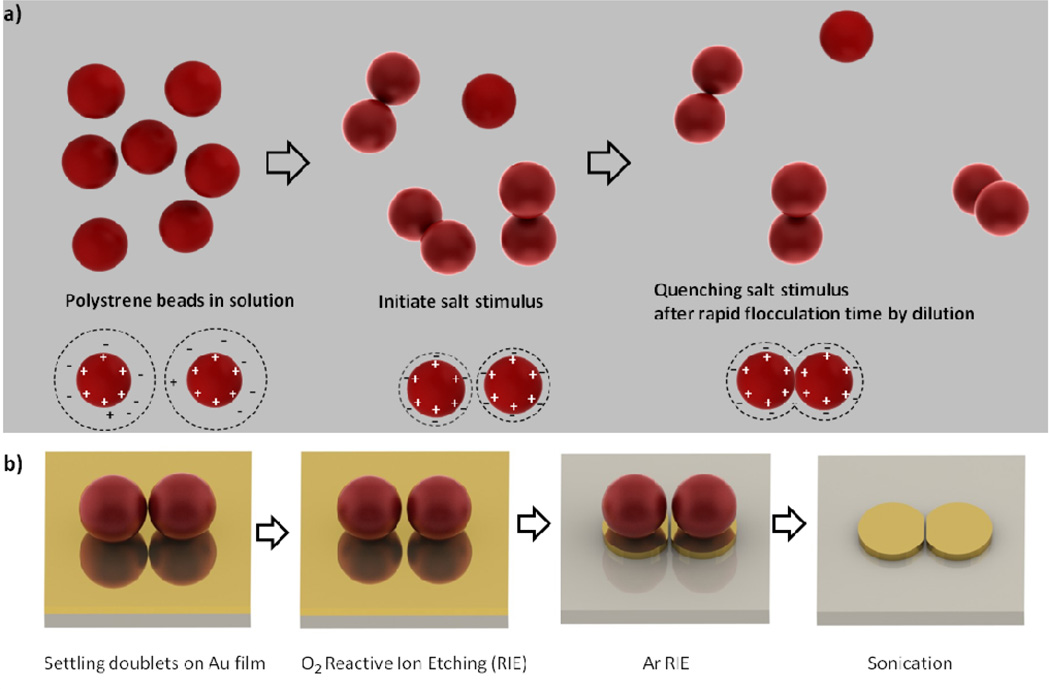
The nanodisk dimers are fabricated in a two-step method. In the first step (scheme 1a), doublets of polystyrene latex beads are fabricated in solution. Doublets of polymeric colloidal particles have been previously synthesized using a variety of techniques;28–32 most of these methods have challenges in either extending the doublet formation to a variety of materials (e.g., metals, polymers, semi-conductors) or scaling the synthesis process with reasonable yields. Recently, a simple and robust technique, salting-out quenching, was developed in our lab to synthesize sub-micron/micron size colloidal doublets by controlled aggregation of colloidal particles.33, 34 This rapid and scalable method relies on temporally controlling interparticle forces35 to achieve doublet formation and has been successfully utilized to synthesize doublets of various materials. The Derjaguin, Landau, Verwey and Overbeek (DLVO) forces35–38 between similarly charged colloidal particles can be made attractive by increasing the ionic strength of the solution, due to the dominance of the van der Waals forces.. The attractive forces lead to aggregation of the particles, which would give large clusters if not properly controlled.39 However, control over the aggregation is obtained by adding de-ionized (DI) water, thus restoring the electrostatic repulsion and “quenching” the aggregation. As shown in scheme 1a, the salting-out quenching process involves increasing the ionic strength of an otherwise stable colloidal solution of positively charged polystyrene latex beads (typically of 200/100 nm in diameter) by initiating a salt stimulus. The increased ionic strength decreases the Debye length of the electric double layer and weakens the inter-particle, charge-based repulsive forces. During the Brownian aggregation process between the polystyrene beads, the beads adhere to one another due to the attractive van der Waals forces. A simple estimate of the time required for the particles to aggregate (and form doublets) is given by the Smoluchowski rapid flocculation equation,38 , where η is the viscosity of the solution, a is the radius of the colloidal particles, k is the Boltzmann constant, T is the temperature of the solution, W is the stability ratio (which identifies how many times particles must collide on average, before they adhere), and ϕ is the volume fraction of particles in the solution. After allowing the diffusion-limited aggregation for a specific duration of time, the “stimulus” is quenched by mixing in a large quantity of DI water, which lowers the ionic strength and prevents further aggregation by restoring the electrostatic repulsion. At this point, the suspension consists primarily of single particles and doublets.
Scheme 1.
Schematic showing (a) synthesis of doublets from polystyrene singlet beads using salting-out quenching technique and (b) fabrication of nanodisk dimers using colloidal lithography, where polystyrene doublets are used as soft masks during etching processes.
In the second step (scheme 1b), we use the doublets fabricated by the salting-out quenching technique to make nanodisk dimers by colloidal lithography. Colloidal lithography uses colloidal beads as masks to fabricate nanoparticles; it is scalable, rapid, and inexpensive. Various plasmonic nanoparticle geometries, including nanoprisms,40, 41 nanorings,42, nanohemishells43, and nanodisk arrays44, 45 have been fabricated using colloidal lithography. These particle geometries, however, were fabricated from isolated beads or with closely packed hexagonally arranged monolayers of beads that do not support large electric fields. Doublets made from the salting-out quenching technique, when used in colloidal lithography, can be used to fabricate nanodisk dimers by transferring the shape of doublets onto a thin metallic film. The process involves using electrostatic interactions to settle polystyrene doublets on a glass slide coated with a thin layer of gold (typically 30 nm) and reducing their diameter by oxygen reactive ion etching (RIE). During the oxygen RIE process, the gold beneath the beads and the distance between the centers of the beads remains unaffected. The reduction of diameter, however, opens up a narrow gap between the polystyrene beads. This is followed by Argon reactive ion etching, where the colloidal doublets act as etch masks, and the gold is removed in the regions that are not covered by the beads. Finally, the beads are removed by sonication to expose the nanodisk dimers on glass substrates. Our method produces nanodisk dimers with excellent tunability in parameters such as nanodisk size, gap, thickness, and choice of metal. This geometric tunability is essential as it helps match the resonance position to excitation light for best performance. In addition to doublets, longer flocculation time will enable higher order aggregates such quadramers and heptamers46, which can be used to fabricate plasmonic clusters that exhibit Fano-like resonances47, 48.
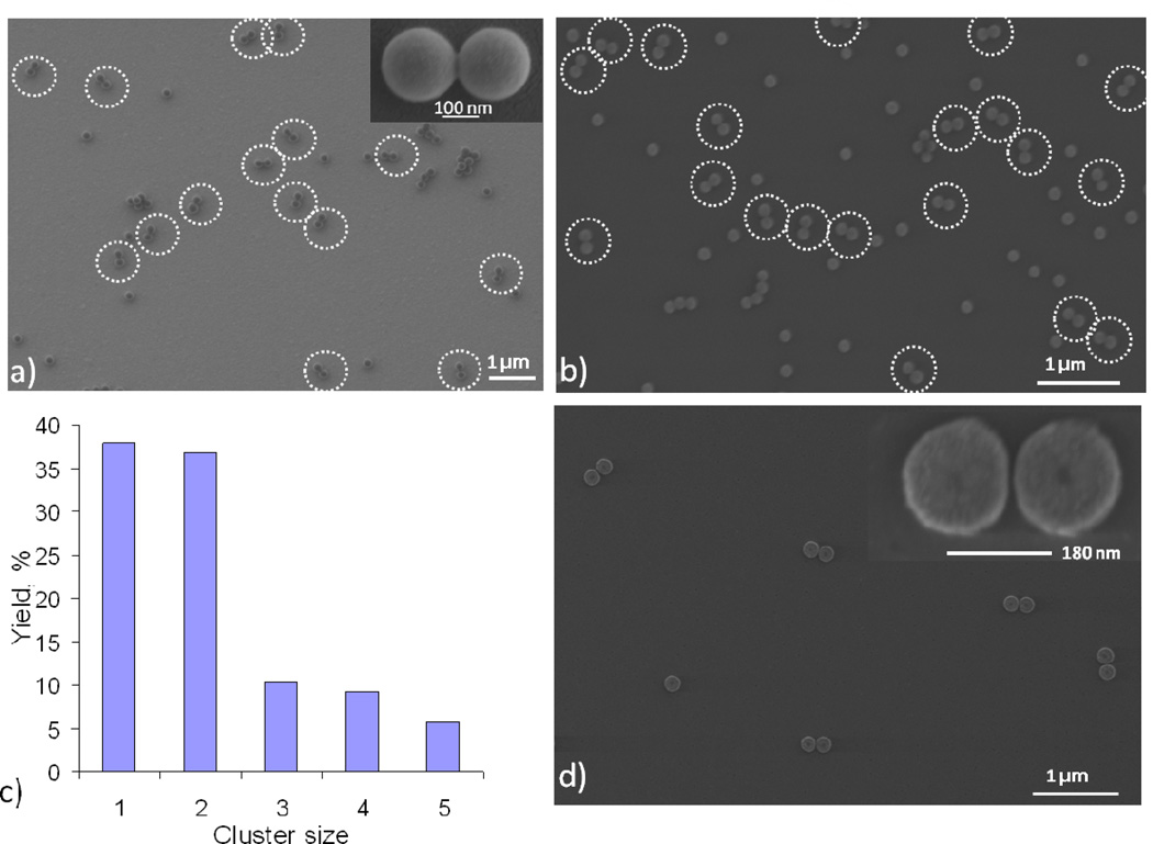
Figures 1a and 1b show representative field emission scanning electron microscopy (FE-SEM) images of polystyrene doublets synthesized with the salting-out-quenching method. Clear contact between two polystyrene beads is seen in all the doublets. Using the salting-out quenching method, we have achieved a reasonably high yield of doublets (~36%), compared to the yield (~1%) without salting-out quenching technique, evidenced by SEM images with >150 particles as shown in Figure 1c. The remaining particles are either isolated or higher order aggregates. The doublet yield could be potentially increased to 70–80%34 by thermally fusing the doublets and further purifying them using density gradient centrifugation49, 50 or hydrodynamic chromatography.51 Separating doublets and higher order aggregates from single particles will be the subject of further studies. Figure 1d shows a representative FE-SEM image of nanodisk dimers resulting from oxygen and Ar RIE process, with an inset showing a magnified view of an individual nanodisk dimer separated by a nanogap.
Figure 1.
FESEM images of polystyrene doublets synthesized using salting-out quenching technique from beads of (a) 200 nm diameter and (b) 100 nm diameter. (c) Yield as function of cluster size after salting-out quenching technique for 200 nm beads. (d) FESEM image of nanodisk dimers fabricated from polystyrene doublets after colloidal lithography. Inset shows enlarged images.
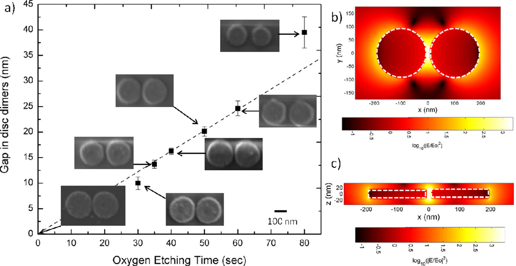
The magnitude of the electric field enhancement and position of the plasmon resonance wavelength in nanodisk dimers strongly depends upon the gap and nanodisk diameter. For surface enhanced Raman spectroscopy applications, it is essential to achieve large electric field enhancements, while simultaneously tuning the plasmon resonance wavelength to match the Raman excitation laser wavelength. Our method allows precise control of the gap/diameter ratio by varying the oxygen RIE time. Longer etch times correspond to smaller beads and subsequently larger gaps between the beads. Figure 2a shows the dependence of the nanogap size on the etch time. In the absence of oxygen etching, the nanodisks touch each other and thus are in the conducting coupled regime.10, 18 Such structures are potentially useful for broad-band energy harvesting applications as proposed by Aubry et al.52, 53 As the RIE time increases, the gap between nanodisks increases from 10 nm to 40 nm with a reasonable standard deviation nearly following a linear trend. A minimum etching time of 30 sec was required to consistently open a 10 nm gap between two polystyrene beads. An etching time interval below 25 sec resulted in two beads still in contact with each other (details can be found in the Supporting Information). Dimer gaps below 10 nm can, in principle, be achieved (not attempted in this current work) by etching for a time interval between 25 and 30 sec. To determine the effects of particle size on electric field intensity with a constant gap, we calculated the electric field intensity distribution and maximum electric field in the nanodisk dimers for various diameters using finite different time domain (FDTD) methods.54 Figure 2b shows electric field distribution at the plasmon resonance frequency for incident light polarized along the dimer axis for a nanodisk dimer geometry corresponding to 30 sec of etching (190 nm disks and separated by 10 nm gap). The figure shows approximately three orders of enhancement in the electric field intensity due to dipole-dipole interaction plasmon modes. The maximum electric field enhancements occur in nanodisk dimers that have large disk diameters and separated by smaller gaps. Such nanodisk dimers can be achieved when larger polystyrene beads are used with short oxygen RIE times.
Figure 2.
(a) Control over nanogap size as a function of oxygen etching time. Insets show representative FESEM images of the nanodisk dimers at various etching times. Calculated electric field intensity distribution in Au nanodisk dimer within (b) in-plane cross-section and (c) out-of-plane cross-section for nanodisk dimer corresponding to 30 sec of oxygen RIE (190 nm diameter, 30 nm height and 10 nm gap) with incident light polarized along the axis of disk dimers.
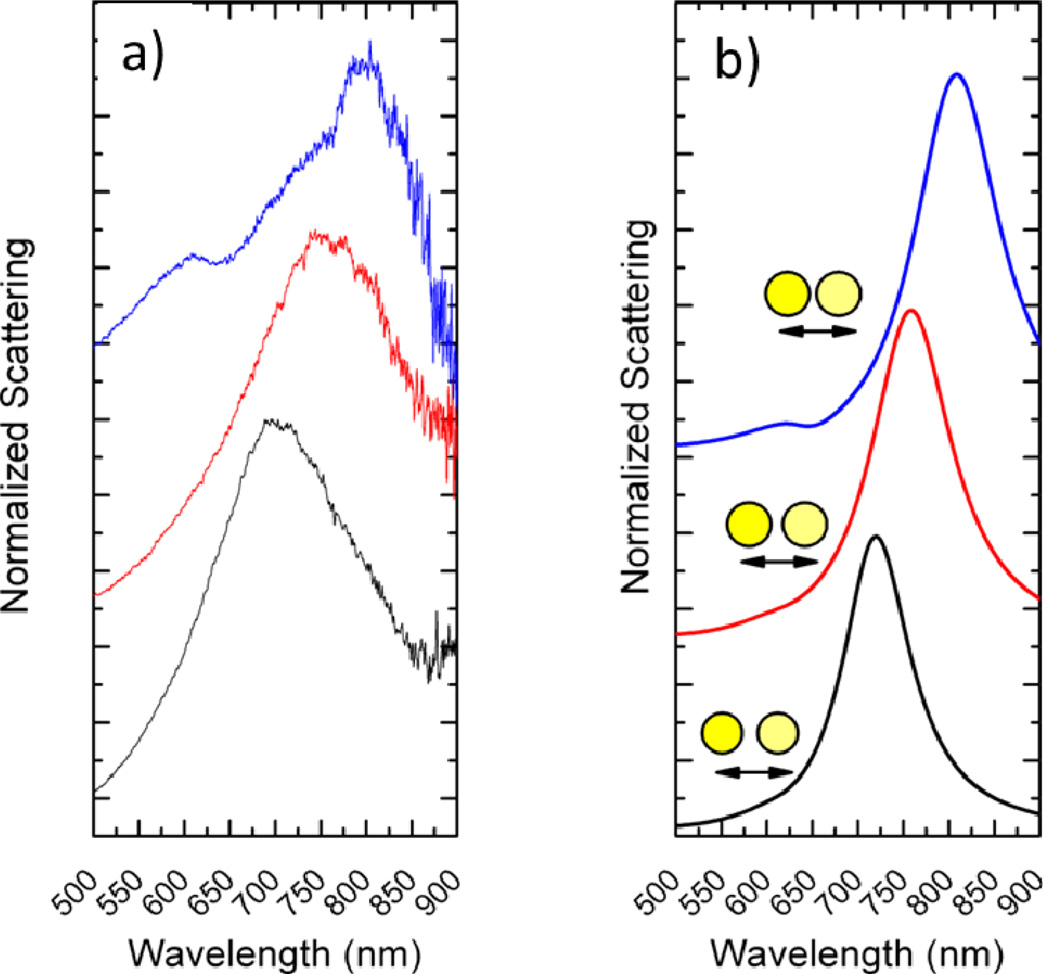
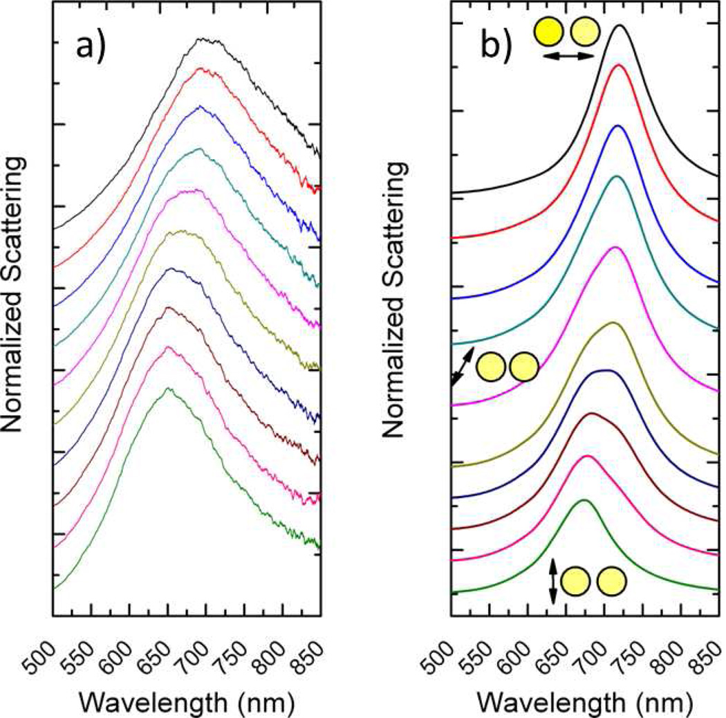
We further investigated the plasmonic resonances of nanodisk dimers using dark field micro-spectroscopy. It has been revealed from previous studies that as the gap between nanoparticle dimers decreases, the dipolar plasmon resonance redshifts due to a decreased restoring force between the charge separations in individual particles.7 To understand the nature of plasmon resonances in these structures, we fabricated nanodisk dimers from 100 nm polystyrene beads. Although nanodisk dimers fabricated from 200 nm polystyrene beads and with short oxygen etch time possess large electric field enhancements, their plasmon resonances are in the infrared range (1200 nm), making their characterization difficult. Figure 3a shows the dark field scattering spectra of nanodisk dimers with various gap/diameter ratio fabricated from 100 nm polystyrene beads and 30 nm thin gold films with light polarized along the axis of dimer. We can see that the longitudinal plasmon peak position blueshifts from 800 nm to 700 nm with increased etch time, a result of increased gap/diameter ratio. To characterize the experimentally observed scattering responses, we performed FDTD simulations of nanodisk dimers with corresponding gap/diameter geometry. The peak positions and widths of the experimentally observed scattering responses (Figure 3b) match well with the FDTD results (Figure 3b). In the case of larger nanodisk diameters with smaller gaps, a quadrapolar plasmon mode at 600 nm emerges in the scattering response of both the experiments and simulations. Plasmon resonances of nanodisk dimers can also be shifted by adjusting the thickness of the film (details can be found in the Supporting Information). In some doublets, the diameter of one bead is slightly larger or smaller than the other. This is due to the inherent size distribution of polystyrene beads following their synthesis by the manufacturer. Even though small, these heterogeneities may affect the plasmon resonances and electric fields in the dimers. Using FDTD calculations, we show (details can be found in the Supporting Information) that heterogeneity changes the peak of the scattering spectra (plasmon resonance) of disc dimer to a lower wavelength, but does not significantly change the magnitude of the electric field that is localized in the dimer gap at plasmon resonance. We also investigated the effect of polarization on the plasmon resonance of the nanodisk dimers. It is known that there are two orthogonal plasmons modes in dimers, one parallel to the dimer axis and other perpendicular. As the polarization changes from parallel to the dimer axis to perpendicular to the dimer axis, these modes are excited at varying degrees. Our results from polarization-dependent dark field spectroscopy are consistent with previous reports as shown in Figure 4a and agree well with FDTD simulations (Figure 4b). With large localization of electric fields, ease of fabrication, and very well defined geometry, the nanodisk dimers fabricated by our method can be readily used as alternatives for large electric field nanostructures fabricated by e-beam lithography or focused ion beam milling. The large electric field exhibited in the gap will be valuable in applications such as SERS sensing, second harmonic and continuum light generation, nanolithography, and microfluidics.
Figure 3.
(a) Experimentally obtained scattering intensity vs. wavelength for nanodisk dimers resulting from 100 nm polystyrene doublets and etched for different time periods (10 sec, 15 sec, 20 sec, from top to bottom). (b) Corresponding FDTD-calculated scattering cross-sections. Incident light is polarized along the axis of the dimer.
Figure 4.
(a) Experimentally obtained scattering intensity vs. wavelength for different polarization angles of incident light (from normal to along the dimer axis in 10°steps) in nanodisk dimer resulting from 100 nm polystyrene doublets with 20 sec of oxygen etching. (b) Corresponding FDTD-calculated scattering cross-section.
In addition to the fabrication of nanodisk dimers, our method can be conveniently modified to fabricate cusp-shaped nanostructures. Such structures, composed of two nanoholes of the same diameter with center-to-center distance smaller than their diameter, were proposed by Reuven Gordon and colleagues.55, 56 Nanoholes in thin metal films have attracted immense interest among researchers after the discovery of extra-ordinary transmission in nanohole arrays by Ebessen et al.57 Various methods, both theoretical and experimental, have been reported in an attempt to understand the origin of this enhanced transmission through single nanoholes in thin films.58–60 A common understanding is that interactions between localized surface plasmons and propagating plasmon modes in these systems dictate the optical performance of the nanoholes. The cusp-shaped nanostructures, when compared to separate nanoholes, exhibit larger electric fields and transmission similar to bowtie slot nanoantennas.61–63 Reuven Gordon and colleagues fabricated arrays of cusp nanostructures by focused ion beam milling in these studies. Large electric fields in cusp nanostructures were also studied by Onuta et al. using second harmonic generation imaging.64 In their study, cusp nanostructures were obtained by random formation of colloidal doublets by using large concentrations of polystyrene beads followed by gold evaporation.
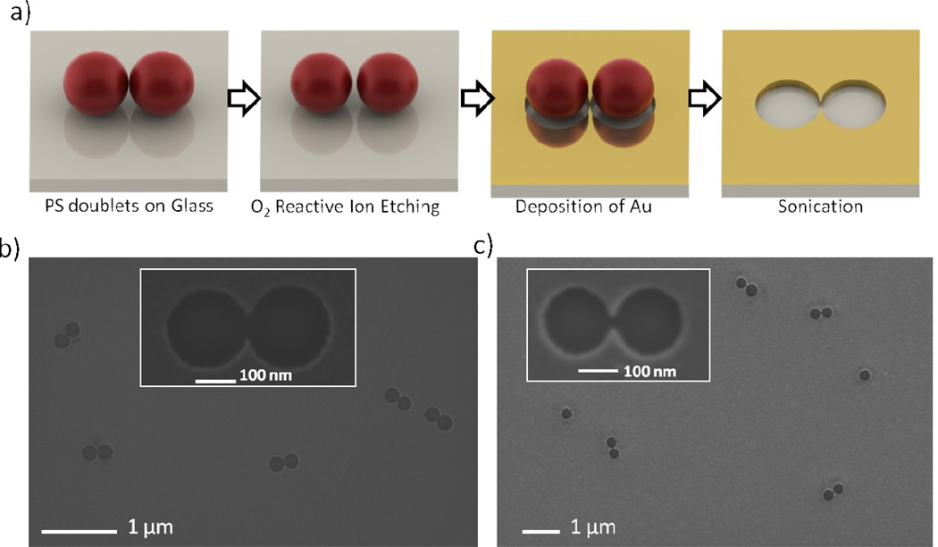
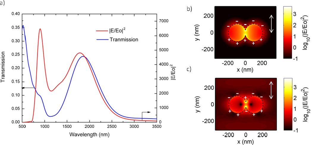
To fabricate cusp-shaped nanostructures (Figure 5a), polystyrene doublets fabricated using the salting-out quenching technique are settled on a glass slide and then etched by oxygen RIE. This etching opens up a gap between the polystyrene beads. A thin film of gold is deposited and the beads are later removed by sonication. Opening a gap between polystyrene beads allows the metal to deposit between beads resulting in the formation of smaller separation between sharp tips in the aperture. Figures 5b and 5c show FESEM images of cusp nanostructures fabricated from 200 nm polystyrene beads using this method without and with oxygen RIE respectively. In the case without oxygen RIE, sharp tips in the aperture are separated by a larger distance than the ones with oxygen etching. Control of the tip separation is important as it dictates the magnitude of the electric field intensity and transmission peak position. To understand the magnitude of electric field enhancements and transmission improvements, we performed FDTD calculations on isolated cusp nanostructures. When excited with an incident light polarized along the axis of the sharp tips, these structures exhibit a sharp transmission peak at 1860 nm with a shoulder at 905 nm (Figure 6a). We also calculated the maximum electric field intensity as a function of wavelength and see that they also peak near these wavelengths. Plots of electric field distribution in the nanostructures at these wavelengths show distinct plasmon modes and represent different charge density distributions as shown in Figures 6b and 6c. The strong transmission peak at lower energy (1860 nm) corresponds to a plasmon mode with electric field spreading throughout the nanostructures, whereas the small shoulder at 905 nm represents a plasmon mode that is tightly confined to the tips. The field distributions and the charge distributions seen in these structures are very similar to the ones reported by Onuta et al. However, the magnitude of the field enhancement in the structures reported here are larger than the ones reported by Onuta et al. This is due to two reasons, 1) the structures reported here are made from smaller polystyrene doublets, and 2) the distance between the two sharp tips is smaller due to oxygen etching of polystyrene beads. These differences lead to larger magnitudes of electric field enhancements, especially at the high energy mode. This is verified by FDTD simulations (details can be found in the Supporting Information), where the effect of disc diameter in cusp structures and distance between two tips on the maximum electric field enhancements is studied. In addition, compared to the earlier studies, the reported fabrication method allows better control of the shape of the cusp nanostructure. Such control is a result of using beads as evaporation templates, which naturally allow uniformity in the shape of the nanoholes and tips. In addition, the possibility to etch polystyrene beads allows fine control over the gap between tips. With enhanced transmission and large localization of electric fields, cusp nanostructures fabricated by our method can be useful in applications such as secondary harmonic light generation,56 highly sensitive chemical sensing,65, 66 and secondary continuum generation.67
Figure 5.
(a) Schematic showing fabrication of cusp nanostructures by using polystyrene doublets as soft masks for evaporation. Representative FESEM images of cusp nanostructures fabricated (b) without oxygen etching and (c) with 15 sec of oxygen etching. Inset shows enlarged images.
Figure 6.
(a) Calculated transmission and maximum electric field intensity vs. wavelength for a nanocusp structure made of nanoholes of 208 nm diameter, 30 nm height and separated by 200 nm gap with incident light polarized along the sharp tips. Electric field intensity distribution in the x-y plane at (b) 1790 nm and (c) 900 nm.
CONCLUSIONS
In summary, we have demonstrated the fabrication of nanodisk dimers and nanocusp structures by the controlled aggregation of polystyrene beads through the salting-out quenching technique and further soft-lithography processing. Our method allows various means of control, such as bead diameter, etch time, and film thickness, which can be employed to finely tune the geometry of the structures and subsequently control their plasmonic properties. Numerical simulations were found to be in good agreement with the experiments. Both nanodisk dimers and nanocusp structures fabricated with our method provide large electric field localization that is geometry and polarization dependent. Our method is rapid, scalable, inexpensive, and results in structures that can be attached to both conducting and non-conducting substrates. We believe that these advantages make our method a promising technique to fabricate nanodisk dimers and nanocusp structures and to be valuable in many applications (such as single molecule detection, second harmonic generation, and broad wavelength energy harvesting) that require plasmonic nanostructures with large electric fields.
MATERIALS AND METHODS
Fabrication of Doublets by Salting-out Quenching Technique
Monodisperse, surfactant-free, amidine-functionalized polystyrene latex (APSL) microspheres (average molecular weight: 70 000 g/mol) were purchased from Invitrogen. Specifically, 100 nm and 200 nm APSL microspheres (2% w/v) were used in the experiments. In order to fabricate 100 (200) nm APSL doublets, 5 µL of APSL colloids were added to 1 mL of 100 (250) mM KCl solution in a centrifuge tube. The rapid flocculation time for this system is approximately 10 sec. This estimate provided a good starting point for forming doublets, and a few rounds of refinement showed that a reaction time of 60 sec for the salting out technique provided enough time for a significant number of doublets to form. The centrifuge tube, with the particles in high ionic strength solution, was rolled for 60 sec, after which 100 mL DI water was added to quench the aggregation, thereby making mostly doublets while limiting the formation of higher order aggregates.
Substrate Preparation
Glass substrates were pre-cleaned by immersion in piranha solution (H2SO4:H2O2 (35%) = 3:1) at 80°C for 30 min and later rinsed with DI water. Samples were further sonicated in H20:NH4OH:H202 (35%) = 5:1:1, rinsed with DI water, and dried with N2 gas.
Fabrication of Nanodisk dimers
Gold was deposited with a Chromium adhesion layer on cleaned glass slides at normal incidence using E-beam evaporation method (Semicore E-gun evaporator). 15 mL of the APSL doublet solution were added to a petridish that contained a precleaned, gold-coated slide, and the particles were allowed to settle for 12 h. The excess liquid and unsettled particles were decanted off, and the dish was washed 8 to 10 times with DI water to remove any particles not strongly attached to the surface. The resulting monolayer of APSL singlets and doublets adhered electrostatically to the gold-coated glass slide. Oxygen RIE (Plasma-Therm 720) was performed at 20 sccm gas flow, 100 mT and 100 W power density for different durations of time. Ar RIE (Plasma-Therm 720) was performed at 30 sccm of argon plasma for 200 sec at 10 mT pressure and 300 W RF generated power. Finally, the slides were sonicated in Toulene/DI Water. The nanodisk dimers were then imaged using Field Emission Scanning Electron Microscope (FESEM JOEL 6700F).
Fabrication of Nanocusp Structures
15 mL of the APSL doublet solution was added to a petridish that contained a cleaned glass slide, and the particles were allowed to settle for 12 h. The excess liquid and unsettled particles were decanted off, and the dish was washed 8 to 10 times with DI water to remove any unadhered particles. Oxygen RIE was performed to etch the polymer colloids at 20 SCCM gas flow, 100 mT and 100 W power density for different time periods. Gold and Chromium layers were deposited at normal incidence using E-beam evaporation method (Semicore E-gun evaporator). Finally, the slides were sonicated in Toulene/DI Water. Cusp Nanostructures were imaged using Field Emission Scanning Electron Microscope (FESEM JOEL 6700F).
Optical Characterization
A transmission mode microscope (Nikon Eclipse TE-2000U) with an oil contact dark-field condenser (NA: 1.3–1.45) and a 100× wet objective with adjustable internal iris were used to obtain scattering spectra of nanodisk dimers. A polarizer was placed at the objective exit to measure polarization dependent scattering.68 The light from the objective was sent to an imaging monochromator (Acton Research MicroSpec 2300i) equipped with a CCD camera (CoolSnap HQ2). Spectra were obtained by collecting samples of light from a region that contained nanodisk dimers (Is) and samples from dark regions (Id). Reference spectra (Ir) were obtained by increasing the iris of objective to allow direct coupling of incident light into the objective. The scattering spectra was obtained by following transformation, (Is-Id)/(Ir-Id) .
Finite Difference Time Domain (FDTD) Method
Plasmonic properties such as size/gap dependent scattering in nanodisk dimers, enhanced transmission in cusp nanostructures, and electric field enhancements in both types of nanostructures were calculated by FDTD method using commercially available software (Lumerical Solution Inc., British Columbia). Perfect matching layers were used to absorb non-physical reflections from the boundaries, and symmetry relations were used to reduce the simulation time. Scattering cross-sections in the case of nanodisk dimers were calculated by a total-field-scattering-field formulation. Both nanodisk dimers and cusp nanostructures were simulated on glass substrates (n=1.45) and exposed to a surrounding environment of water (n=1.33). Plane wave sources were incident from the glass slide and scattering/transmission monitors were placed in the surrounding medium. The experimental dielectric function of gold69 was fitted by a polynomial with 10 coefficients and used for all the simulations.
Supplementary Material
Acknowledgements
We gratefully acknowledge the help from B. Kiraly in manuscript preparation and the financial support from Air Force Office of Scientific Research (AFOSR), NIH Director’s New Innovator Award (1DP2OD007209-01), National Science Foundation (0824183, and 0801922), and the Penn State Center for Nanoscale Science (MRSEC). Components of this work were conducted at the Penn State node of the NSF-funded National Nanotechnology Infrastructure Network.
Footnotes
Supporting Information Available: Information related to: 1) minimum oxygen etching time to open a dimer gap, 2) effect of diameter heterogeneity on plasmon resonances and electric fields in nanodisc dimers, 3) effect of thickness on plasmon resonances in nanodisc dimers, and 4) effect of nanohole diameters and oxygen etching on electric field enhancements in cusp nanostructures are provided in the supporting information. This material is available free of charge via the Internet at http://pubs.acs.org.
REFERENCES
- 1.Zuloaga J, Nordlander P. On the Energy Shift Between Near-Field and Far-Field Peak Intensities in Localized Plasmon Systems. Nano Lett. 2011;11:1280–1283. doi: 10.1021/nl1043242. [DOI] [PubMed] [Google Scholar]
- 2.Maier SA, Atwater HA. Plasmonics: Localization and Guiding of Electromagnetic Energy in Metal/dielectric Structures. J. Appl. Phys. 2005;98:011101. [Google Scholar]
- 3.Halas NJ. Plasmonics: An Emerging Field Fostered by Nano Letters. Nano Lett. 2010;10:3816–3822. doi: 10.1021/nl1032342. [DOI] [PubMed] [Google Scholar]
- 4.Link S, El-Sayed MA. Size and Temperature Dependence of the Plasmon Absorption of Colloidal Gold Nanoparticles. J. Phys. Chem. B. 1999;103:4212–4217. [Google Scholar]
- 5.Zheng YB, Yang YW, Jensen L, Fang L, Juluri BK, Flood AH, Weiss PS, Stoddart JF, Huang TJ. Active Molecular Plasmonics: Controlling Plasmon Resonances with Molecular Switches. Nano Lett. 2009;9:819–825. doi: 10.1021/nl803539g. [DOI] [PubMed] [Google Scholar]
- 6.Mayer KM, Lee S, Liao H, Rostro BC, Fuentes A, Scully PT, Nehl CL, Hafner JH. A Label-Free Immunoassay Based upon Localized Surface Plasmon Resonance of Gold Nanorods. ACS Nano. 2008;2:687–692. doi: 10.1021/nn7003734. [DOI] [PubMed] [Google Scholar]
- 7.Rechberger W, Hohenau A, Leitner A, Krenn JR, Lamprecht B, Aussenegg FR. Optical Properties of Two Interacting Gold Nanoparticles. Opt. Commun. 2003;220:137–141. [Google Scholar]
- 8.Lassiter JB, Aizpurua J, Hernandez LI, Brandl DW, Romero I, Lal S, Hafner JH, Nordlander P, Halas NJ. Close Encounters Between Two Nanoshells. Nano Lett. 2008;8:1212–1218. doi: 10.1021/nl080271o. [DOI] [PubMed] [Google Scholar]
- 9.Futamata M, Maruyama Y, Ishikawa M. Local Electric Field and Scattering Cross Section of Ag Nanoparticles Under Surface Plasmon Resonance by Finite Difference Time Domain Method. J. Phys. Chem. B. 2003;107:7607–7617. [Google Scholar]
- 10.Slaughter LS, Wu Y, Willingham BA, Nordlander P, Link S. Effects of Symmetry Breaking and Conductive Contact on the Plasmon Coupling in Gold Nanorod Dimers. ACS Nano. 2010;4:4657–4666. doi: 10.1021/nn1011144. [DOI] [PubMed] [Google Scholar]
- 11.Jiang J, Bosnick K, Maillard M, Brus L. Single Molecule Raman Spectroscopy at the Junctions of Large Ag Nanocrystals. J. Phys. Chem. B. 2003;107:9964–9972. [Google Scholar]
- 12.Xu H, Bjerneld EJ, Kall M, Borjesson L. Spectroscopy of Single Hemoglobin Molecules by Surface Enhanced Raman Scattering. Phys. Rev. Lett. 1999;83:4357–4360. [Google Scholar]
- 13.Ringler M, Schwemer A, Wunderlich M, Nichtl A, Kurzinger K, Klar T, Feldmann J. Shaping Emission Spectra of Fluorescent Molecules with Single Plasmonic Nanoresonators. Phys. Rev. Lett. 2008;100:1–4. doi: 10.1103/PhysRevLett.100.203002. [DOI] [PubMed] [Google Scholar]
- 14.Ko KD, Kumar A, Fung KH, Ambekar R, Liu GL, Fang NX, Toussaint KC. Nonlinear Optical Response from Arrays of Au Bowtie Nanoantennas. Nano Lett. 2011;11:61–65. doi: 10.1021/nl102751m. [DOI] [PubMed] [Google Scholar]
- 15.Kim S, Jin J, Kim YJ, Park IY, Kim Y, Kim SW. High-Harmonic Generation by Resonant Plasmon Field Enhancement. Nature. 2008;453:757–760. doi: 10.1038/nature07012. [DOI] [PubMed] [Google Scholar]
- 16.Muskens OL, Giannini V, Sanchez-Gil JA, Gomez Rivas J. Optical Scattering Resonances of Single and Coupled Dimer Plasmonic Nanoantennas. Opt. Express. 2007;15:17736–17746. doi: 10.1364/oe.15.017736. [DOI] [PubMed] [Google Scholar]
- 17.Su K, Wei Q, Zhang X. Interparticle Coupling Effects on Plasmon Resonances of Nanogold Particles. Nano Lett. 2003;3:1087–1090. [Google Scholar]
- 18.Atay T, Song J, Nurmikko AV. Strongly Interacting Plasmon Nanoparticle Pairs : From Dipole-Dipole Interaction to Conductively Coupled Regime. Nano Lett. 2004;4:1627–1631. [Google Scholar]
- 19.Aksu S, Yanik AA, Adato R, Artar A, Huang M, Altug H. High-Throughput Nanofabrication of Infrared Plasmonic Nanoantenna Arrays for Vibrational Nanospectroscopy. Nano Lett. 2010;10:2511–2518. doi: 10.1021/nl101042a. [DOI] [PubMed] [Google Scholar]
- 20.Brown LV, Sobhani H, Lassiter JB, Nordlander P, Halas NJ. Heterodimers: Plasmonic Properties of Mismatched Nanoparticle Pairs. ACS Nano. 2010;4:819–832. doi: 10.1021/nn9017312. [DOI] [PubMed] [Google Scholar]
- 21.Maneeprakorn W, Malik MA, O’Brien P. Developing Chemical Strategies for the Assembly of Nanoparticles into Mesoscopic Objects. J. Am. Chem. Soc. 2010;132:1780–1781. doi: 10.1021/ja910022q. [DOI] [PubMed] [Google Scholar]
- 22.Novak JP, Feldheim DL. Assembly of Phenylacetylene-Bridged Silver and Gold Nanoparticle Arrays. J. Am. Chem. Soc. 2000;122:3979–3980. [Google Scholar]
- 23.Sonnichsen C, Reinhard BM, Liphardt J, Alivisatos AP. A Molecular Ruler Based on Plasmon Coupling of Single Gold and Silver Nanoparticles. Nat. Biotechnol. 2005;23:741–745. doi: 10.1038/nbt1100. [DOI] [PubMed] [Google Scholar]
- 24.Li W, Camargo PHC, Lu X, Xia Y. Dimers of Silver Nanospheres : Facile Synthesis and Their Use As Hot Spots for Surface-Enhanced Raman Scattering. Nano Lett. 2009;9:485–490. doi: 10.1021/nl803621x. [DOI] [PMC free article] [PubMed] [Google Scholar]
- 25.Worden JG, Shaffer AW, Huo Q. Controlled Functionalization of Gold Nanoparticles Through a Solid Phase Synthesis Approach. Chem. Commun. 2004;2004:518–519. doi: 10.1039/b312819a. [DOI] [PubMed] [Google Scholar]
- 26.Sardar R, Heap TB, Shumaker-Parry JS. Versatile Solid Phase Synthesis of Gold Nanoparticle Dimers Using an Asymmetric Functionalization Approach. J. Am. Chem. Soc. 2007;129:5356–5357. doi: 10.1021/ja070933w. [DOI] [PubMed] [Google Scholar]
- 27.Wang X, Li G, Chen T, Yang M, Zhang Z, Wu T, Chen H. Polymer-Encapsulated Gold- Nanoparticle Dimers: Facile Preparation and Catalytical Application in Guided Growth of Dimeric ZnO-Nanowires. Nano Lett. 2008;8:2643–2647. doi: 10.1021/nl080820q. [DOI] [PubMed] [Google Scholar]
- 28.Hiddessen AL, Rodgers SD, Weitz DA, Hammer DA. Assembly of Binary Colloidal Structures Via Specific Biological Adhesion. Langmuir. 2000;16:9744–9753. doi: 10.1021/la036416i. [DOI] [PubMed] [Google Scholar]
- 29.Hosein ID, Liddell CM. Convectively Assembled Asymmetric Dimer-Based Colloidal Crystals. Langmuir. 2007;23:10479–10485. doi: 10.1021/la7007254. [DOI] [PubMed] [Google Scholar]
- 30.Liddell CM, Summers CJ. Monodispersed ZnS Dimers, Trimers, and Tetramers for Lower Symmetry Photonic Crystal Lattices. Adv. Mater. 2003;15:1715–1719. [Google Scholar]
- 31.Yi GR, Manoharan VN, Michel E, Elsesser MT, Yang SM, Pine DJ. Colloidal Clusters of Silica or Polymer Microspheres. Adv. Mater. 2004;16:1204–1208. [Google Scholar]
- 32.Yin Y, Lu Y, Gates B, Xia Y. Template-Assisted Self-Assembly: A Practical Route to Complex Aggregates of Monodispersed Colloids with Well-Defined Sizes, Shapes, and Structures. J. Am. Chem. Soc. 2001;123:8718–8729. doi: 10.1021/ja011048v. [DOI] [PubMed] [Google Scholar]
- 33.McDermott JJ, Velegol D. Simple Fabrication of Metallic Colloidal Doublets Having Electrical Connectivity. Langmuir. 2008;24:4335–4339. doi: 10.1021/la703894v. [DOI] [PubMed] [Google Scholar]
- 34.Yake AM, Panella R, Snyder CE, Velegol D. Fabrication of Colloidal Doublets by a Salting Out-Quenching-Fusing Technique. Langmuir. 2006;22:9135–9141. doi: 10.1021/la061339n. [DOI] [PubMed] [Google Scholar]
- 35.Israelachvilli JN. Intermolecular and Surface Forces. 2nd ed. New York: Academic Press; 1992. [Google Scholar]
- 36.Deraguin BV, Landau LD. Theory of the Stability of Strongly Charged Lyophobic Sols and of the Adhesion of Strongly Charged Particles in Solution of Electrolytes. Acta Physicochim:USSR. 1941;14:633–662. [Google Scholar]
- 37.Verwey EJW, Overbeek JTG. Theory of the Stability of Lyophobic Colloids. Amsterdam: Elsevier; 1948. [Google Scholar]
- 38.Russel W, Saville D, Schowalter W. Colloidal Dispersions. Cambride University Press; 1989. [Google Scholar]
- 39.Larmour IA, Faulds K, Graham D. Improved Versatility of Silver Nanoparticle Dimers for Surface-Enhanced Raman Spectroscopy. J. Phys. Chem. C. 2010;114:13249–13254. [Google Scholar]
- 40.Haynes CL, Van Duyne RP. Nanosphere Lithography: A Versatile Nanofabrication Tool for Studies of Size-Dependent Nanoparticle Optics. J. Phys. Chem. B. 2001;105:5599–5611. [Google Scholar]
- 41.Malinsky MD, Kelly KL, Schatz GC, Van Duyne RP. Nanosphere Lithography: Effect of Substrate on the Localized Surface Plasmon Resonance Spectrum of Silver Nanoparticles. J. Phys. Chem. B. 2001;105:2343–2350. [Google Scholar]
- 42.Aizpurua J, Hanarp P, Sutherland DS, Kall M, Bryant GW, Garcia de Abajo FJ. Optical Properties of Gold Nanorings. Phys. Rev. Lett. 2003;90:5–8. doi: 10.1103/PhysRevLett.90.057401. [DOI] [PubMed] [Google Scholar]
- 43.Zheng YB, Huang TJ, Desai AY, Wang SJ, Tan LK, Gao H, Huan ACH. Thermal Behavior of Localized Surface Plasmon Resonance of Au/TiO_2 Core/shell Nanoparticle Arrays. Appl. Phys. Lett. 2007;90:183117. [Google Scholar]
- 44.Zheng YB, Juluri BK, Jensen LL, Ahmed D, Lu M, Jensen L, Huang TJ. Dynamic Tuning of Plasmon-Exciton Coupling in Arrays of Nanodisk-J-Aggregate Complexes. Adv. Mater. 2010;22:3603–3607. doi: 10.1002/adma.201000251. [DOI] [PubMed] [Google Scholar]
- 45.Zheng YB, Juluri BK, Mao X, Walker TR, Huang TJ. Systematic Investigation of Localized Surface Plasmon Resonance of Long-Range Ordered Au Nanodisk Arrays. J. Appl. Phys. 2008;103:014308. [Google Scholar]
- 46.Higashitani K, Matsuno Y. Rapid Brownian Coagulation of Colloidal Dispersions. J. Chem. Eng. Jpn. 1979;12:460–465. [Google Scholar]
- 47.Fan JA, Bao K, Wu C, Bao J, Bardhan R, Halas NJ, Manoharan VN, Shvets G, Nordlander P, Capasso F. Fano-like Interference in Self-Assembled Plasmonic Quadrumer Clusters. Nano Lett. 2010;10:4680–4685. doi: 10.1021/nl1029732. [DOI] [PubMed] [Google Scholar]
- 48.Fan JA, Wu C, Bao K, Bao J, Bardhan R, Halas NJ, Manoharan VN, Nordlander P, Shvets G, Capasso F. Self-Assembled Plasmonic Nanoparticle Clusters. Science. 2010;328:1135–1138. doi: 10.1126/science.1187949. [DOI] [PubMed] [Google Scholar]
- 49.Manoharan VN, Elsesser MT, Pine DJ. Dense Packing and Symmetry in Small Cluster OF Microspheres. Science. 2003;301:483–487. doi: 10.1126/science.1086189. [DOI] [PubMed] [Google Scholar]
- 50.Price CA. Centrifugation in Density Gradients. New York: Academic Press; 1982. [Google Scholar]
- 51.VandeVen TGM. Colloidal Hydrodynamics. San Diego: Academic Press; 1989. [Google Scholar]
- 52.Aubry A, Lei DY, Maier SA, Pendry JB. Interaction Between Plasmonic Nanoparticles Revisited with Transformation Optics. Phys. Rev. Lett. 2010;105:2–5. doi: 10.1103/PhysRevLett.105.233901. [DOI] [PubMed] [Google Scholar]
- 53.Lei DY, Aubry A, Luo Y, Maier SA, Pendry JB. Plasmonic Interaction Between Overlapping Nanowires. ACS Nano. 2010;5:597–607. doi: 10.1021/nn102819p. [DOI] [PubMed] [Google Scholar]
- 54.Taflove A, Hagness S. Computational Electrodynamics: The Finite-Difference Time-Domain Method. Norwood: Artech House; 2000. [Google Scholar]
- 55.Kumar LKS, Lesuffleur A, Hughes MC, Gordon R. Double Nanohole Apex-Enhanced Transmission in Metal Films. Appl. Phys. B. 2006;84:25–28. [Google Scholar]
- 56.Lesuffleur A, Kumar LKS, Gordon R. Enhanced Second Harmonic Generation from Nanoscale Double-Hole Arrays in a Gold Film. Appl. Phys. Lett. 2006;88:261104. [Google Scholar]
- 57.Ebbesen TW, Lezec HJ, Ghaemi HF, Thio T, Wolff PA. Extraordinary Optical Transmission Through Sub-Wavelength Hole Arrays. Nature. 1998;391:667–669. [Google Scholar]
- 58.Hao Q, Zeng Y, Wang X, Zhao Y, Wang B, Chiang I-K, Werner DH, Crespi V, Huang TJ. Characterization of Complementary Patterned Metallic Membranes Produced Simultaneously by a Dual Fabrication Process. Appl. Phys. Lett. 2010;97:193101. [Google Scholar]
- 59.Chang SH, Gray S, Schatz G. Surface Plasmon Generation and Light Transmission by Isolated Nanoholes and Arrays of Nanoholes in Thin Metal Films. Opt. Express. 2005;13:3150–3165. doi: 10.1364/opex.13.003150. [DOI] [PubMed] [Google Scholar]
- 60.Park TH, Mirin N, Lassiter JB, Nehl CL, Halas NJ, Nordlander P. Optical Properties of a Nanosized Hole in a Thin Metallic Film. ACS Nano. 2008;2:25–32. doi: 10.1021/nn700292y. [DOI] [PubMed] [Google Scholar]
- 61.Wang L, Uppuluri SM, Jin EX, Xu X. Nanolithography Using High Transmission Nanoscale Bowtie Apertures. Nano Lett. 2006;6:361–364. doi: 10.1021/nl052371p. [DOI] [PubMed] [Google Scholar]
- 62.Wang L, Xu X. High Transmission Nanoscale Bowtie-Shaped Aperture Probe for Near-Field Optical Imaging. Appl. Phys. Lett. 2007;90:261105. [Google Scholar]
- 63.Wang L, Xu X. Spectral Resonance of Nanoscale Bowtie Apertures in Visible Wavelength. Appl. Phys. A. 2007;89:293–297. [Google Scholar]
- 64.Onuta TD, Waegele M, DuFort CC, Schaich WL, Dragnea B. Optical Field Enhancement at Cusps Between Adjacent Nanoapertures. Nano Lett. 2007;7:557–564. doi: 10.1021/nl0621600. [DOI] [PubMed] [Google Scholar]
- 65.Yanik AA, Huang M, Artar A, Chang T-Y, Altug H. Integrated Nanoplasmonic- Nanofluidic Biosensors with Targeted Delivery of Analytes. Appl. Phys. Lett. 2010;96:021101. [Google Scholar]
- 66.Lesuffleur A, Im H, Lindquist NC, Oh SH. Periodic Nanohole Arrays with Shape- Enhanced Plasmon Resonance As Real-Time Biosensors. Appl. Phys. Lett. 2007;90:243110. [Google Scholar]
- 67.Muhlschlegel P, Eisler HJ, Martin OJF, Hecht B, Pohl DW. Resonant Optical Antennas. Science. 2005;308:1607–1609. doi: 10.1126/science.1111886. [DOI] [PubMed] [Google Scholar]
- 68.Sheikholeslami S, Jun YW, Jain PK, Alivisatos AP. Coupling of Optical Resonances in a Compositionally Asymmetric Plasmonic Nanoparticle Dimer. Nano Lett. 2010;10:2655–2660. doi: 10.1021/nl101380f. [DOI] [PubMed] [Google Scholar]
- 69.Johnson PB, Christy RW. Optical Constants of the Noble Metals. Phys. Rev. B. 1972;6:4370–4379. [Google Scholar]
Associated Data
This section collects any data citations, data availability statements, or supplementary materials included in this article.


