Abstract
We have fabricated porous silicon nanopillar arrays over large areas with a rapid, simple, and low-cost technique. The porous silicon nanopillars show unique longitudinal features along their entire length and have porosity with dimensions on the single-nanometer scale. Both Raman spectroscopy and photoluminescence data were used to determine the nanocrystallite size to be < 3 nm. The porous silicon nanopillar arrays also maintained excellent ensemble properties, reducing reflection nearly fivefold from planar silicon in the visible range without any optimization and approaching superhydrophobic behavior with increasing aspect ratio, demonstrating contact angles up to 138°. Finally, the porous silicon nanopillar arrays were made into sensitive surface enhanced Raman scattering (SERS) substrates by depositing metal onto the pillars. The SERS performance of the substrates was demonstrated using a chemical dye Rhodamine 6G. With their multitude of properties (i.e., antireflection, superhydrophobicity, photoluminescence, and sensitive SERS), the porous silicon nanopillar arrays described here can be valuable in applications such as solar harvesting, electrochemical cells, self-cleaning devices, and dynamic biological monitoring.
1. Introduction
Reducing the dimensions of bulk materials to the nanometer-scale can introduce unique characteristics strongly related to the size of the structures. For example, porous silicon and silicon nanowires and nanopillars have demonstrated that nanoscale dimensions can correspond to important fundamental changes in the electronic band structure of the material, which can influence electronic, optical, and thermal material properties [1–9]. A large number of these studies have been motivated by the possibility of light emission from silicon-based materials, as it presents an attractive opportunity to bridge current gaps between photonic and electronic circuits [10–12]. Indeed, both porous silicon and silicon nanowires have demonstrated luminescent properties, generally attributed to quantum confinement of the electron wave functions inside the nanosized material [13–19]. In a similar regard, nanoscale dimensions can also effectively confine lattice vibrations, or phonons, to significantly alter heat dissipation and improve thermoelectric performance [20,21]. Finally, decreased nanostructure size corresponds to increases in the surface area to volume ratio, which have been exploited for a variety of biochemical surface-based sensing techniques [22–30]. Strong interest in silicon-based nanostructures will continue while it remains the major workhorse of the microelectronics industry.
Both porous silicon and silicon nanopillar/nanowires have been fabricated with nanoscale dimensions during wet etching in the presence of bulk silicon. Generally, a galvanic cell is used to drive an electrochemical reaction to form porous silicon from single-crystalline Si wafers [25]. The porosity is usually initiated at energetically favorable nucleation sites, where a locally enhanced etch rate leads to nanoscale porosity [31]. Metal-catalyzed chemical etching has also demonstrated the production of porous silicon using a random network of metal nanoparticles to define pore etching sites [32,33]. The metal acts as a carrier transport layer to locally remove charge from the adjacent silicon, making it vulnerable to a chemical etchant [34,35]. Nanopatterned metals have utilized this principle to produce ordered arrays of one-dimensional silicon nanostructures by creating relief in a flat Si wafer surface [36–38]. Although improvements in nanofabrication have steadily decreased the size of these nanostructures, it is still difficult to produce uniform size distributions in the sub-10 nm regime where quantum confinement becomes relevant [18,39].
In this regard, multiscale porous nanostructures with size on the order of hundreds of nanometers and porosity on the order of single nanometers can bridge the gap between the mesoscopic and quantum regimes. Although both porous silicon and silicon nanopillars/nanowires have been thoroughly studied [31,40–48], limited studies have been conducted on the combine system, i.e., porous silicon nanopillars. Such a combine system offers the unique possibility of integrating advantages from multiple length scales into a single material or device. Deep subwavelength (<10 nm) porosity, for instance, can have significant effects on the electronic and optical properties of the materials, while wavelength-scale periodicity can affect mechanical and optical surface properties including wetting and reflection [49,50]. Structures with such diverse properties offer exciting potential for use in a variety of applications including optoelectronics, optomechanics, electromechanics, and a number of sensing-based systems [41–53].
In this work, we developed a multifunctional nanoporous silicon nanopillar array through a simple fabrication procedure and characterized it for a variety of potential applications in biology, chemistry, optics, and electronics. Our method can fabricate highly uniform nanoporous silicon nanopillars with ordered arrays covering up to cm2, and it can be realized at very low-cost—an important feature for a variety of potential applications. The pillars reported here have several unique characteristics, including sharp, longitudinal grooves from the metallic mask and nanometer-scale porosity. The nanoporous silicon nanopillar arrays demonstrate a reduction in the reflection from a polished Si wafer and a strong resistance to wetting by water-based solutions due to the long-range periodic nature of the nanopillar array. They were further used as sensitive surface enhanced Raman scattering (SERS) substrates after the deposition of a metal coating. This work demonstrates the versatility of porous silicon nanopillar substrates, and discusses their potential applications in sensors, solar cells, electronics, electrochemical cells, and self-cleaning devices.
2. Experimental details
Fabrication Procedure
The porous silicon nanopillar arrays were fabricated in two major steps: nanosphere lithography [54–57] to fabricate a hexagonal nanohole array in a thin gold film (Fig. 1a–1d) and a subsequent wet chemical etch of the underlying (100) silicon substrate (Fig. 1e). Each step involved in the fabrication procedure (e.g., nanosphere self-assembly, reactive ion etching, metal-catalyzed silicon etch, metal deposition) is described in detail in the following sections. We demonstrate that this procedure can be used to introduce single-nanometer scale porosity and surface features to the nanostructures (Fig. 1f).
Figure 1.
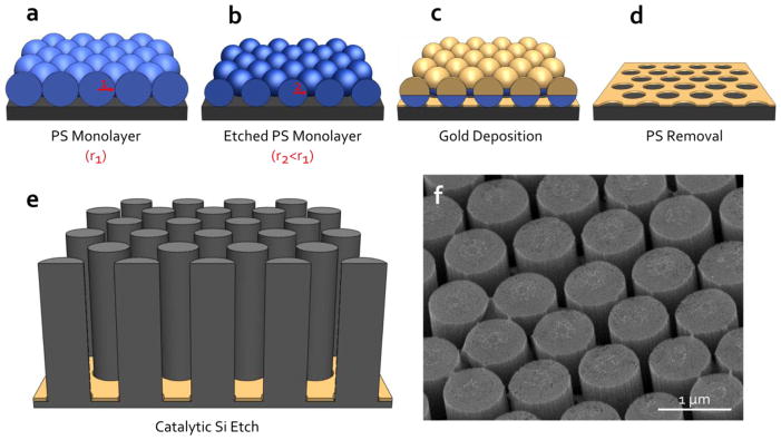
Schematic of the porous silicon nanopillar fabrication procedure: (a) formation of a monolayer of polystyrene (PS) nanospheres, (b) nanosphere etching via reactive ion etching, (c) gold deposition, (d) bead removal, and (e) catalytic chemical etch of the underlying silicon substrate. (f) Tilted SEM image of a porous silicon nanopillar array.
Nanosphere Self-Assembly
In nanosphere self-assembly, the polystyrene monolayer was prepared as previously reported [58–67]. First, Corning glass microscope slides were cut into approximately 1″ squares and ultrasonicated for 1 h in piranha (3:1 H2SO4:H2O2) then 1 h in RCA1 (5:1:1 H2O:NH4OH: H2O2) to thoroughly clean the surface. Later procedures substituted extensive plasma cleaning (20 min in a Harrick Plasma Cleaner at approximately 10.15 W) to achieve comparable surface cleanliness as seen through surface wetting.
The freshly cleaned, superhydrophilic glass slides were mounted into a spin coater with 10–20 μL of stock 1 μm polystyrene beads from Bangs Laboratories. A uniform coating of the beads was achieved by slowly dispersing the beads onto the substrate in a spiral pattern outward from the center. The substrate was then spun between 400 and 600 rpm for 3 min until the majority of the solvent had evaporated. The liquid remaining at the corners was removed with a lint-free tissue. The dried substrate was then slowly immersed into deionized water at an angle of approximately 60° to the surface normal. A polystyrene monolayer was detached from the sample surface and allowed to float on top of the liquid surface. The monolayer was picked up by a piece of a silicon (100) wafer that had been sonicated in ethanol for 10 min. Finally, the silicon substrate and monolayer system was allowed to completely dry in air.
Reactive Ion Etching and Gold Deposition
Before reactive ion etching (RIE), the samples were heated to 110 °C for 10 min to affix their lattice positions by inducing a slight material deformation. A Plasma-Therm 720 was used with various etch time (0.5–5 min), RF power (75–125 W), and base pressure (20–80 mTorr) to reduce the diameter of the polystyrene spheres. Scanning electron microscopy (SEM) (Zeiss Leo 1530) was used to characterize the etch results and examine the resulting surface roughness. Gold was deposited in a Kurt J. Leskar Electron-Beam Evaporation system at base pressures below 2 × 10⁻⁶ Torr; the gold films used for the chemical etch were 10 nm thick and deposited at 0.5 Å/s. Optionally, the polystyrene nanosphere template was removed via scotch tape or sonication in CH2Cl2.
Metal-Catalyzed Silicon Etch
The etchant solution was prepared by adding 160 mL of deionized water to a plastic container, followed by 40 mL of 49% HF and 2 mL of 30% H2O2. During the etch, bubbles were periodically removed from the surface of the samples via gentle agitation in efforts to ensure a homogenous etch. The etch was monitored using the change in color of the silicon substrates, gradually getting darker with increased etch time. Finally, samples were taken out after a specified amount of time (30, 60, or 90 min) and thoroughly rinsed with deionized water and dried.
Optical Measurements
Contact angle measurements were taken with a commercial wetting angle apparatus (FTA 1000B, First Ten Angstroms) equipped with a rotational stage and video camera. The experiments were carried out in ambient laboratory conditions without control of the relative humidity. To measure each static contact angle, a 10 μL droplet was carefully placed on the desired substrate; after a brief pause to let the system equilibrate, the image of the droplet was taken. The contact angle was determined both by the commercial software package included in the wetting angle apparatus and a free software package: ImageJ. Reflection measurements of the porous silicon nanopillar arrays were taken with a Perkin-Elmer Lambda 950 UV-VIS-NIR Spectrophotometer. A specialized accessory allowed the instantaneous collection of the absolute reflectance between 300 and 800 nm. The sample collection area was approximately 4 mm × 4 mm and covered a small portion of the porous silicon nanopillar substrate.
Metal Deposition and SERS Experiments
Two methods were attempted to deposit a thin conformal metal film onto the porous silicon nanopillar substrates. The first was an electrochemical method which used a two-electrode configuration driven by a constant potential. The electrolyte solution was prepared by dissolving 0.4 g AgNO3 and 0.4 g H3BO3 into 40 ml deionized water. The silicon nanopillar array served as the working electrode with a piece of Pt foil used for the counter electrode. All of the samples were driven with a potential of 2 V for 2 min. The second method utilized a thin film sputter coater (Bal-Tec 050 Sputter Coater) without substrate biasing to deposit approximately 20 nm of gold. The gold was sputtered below 5 × 10⁻⁵ in three 180 s intervals to ensure that the system did not build up too much heat. Additionally, the gold-sputtered substrate was heated to 500 °C to alter the film morphology on the pillar surfaces.
To prepare the substrates for SERS measurements, they were incubated in 1 μM of a Rhodamine 6G (R6G) dye overnight and then rinsed with water to ensure monolayer of R6G molecules attached. The SERS measurements were made on a WITec CRM 200 Confocal MicroRaman system equipped with four laser lines. All the measurements taken in this report used a 488 nm laser with a 40× objective. A DV401A-BV He cooled CCD was used in conjunction with a PI Acton 2300i Spectrograph to collect the IR spectra with a resolution of approximately 0.39 nm. Finally the laser power used in the experiment varied from 15 to 30 mW.
3. Results and discussion
Fabrication and Characterization of Porous Silicon Nanopillar arrays
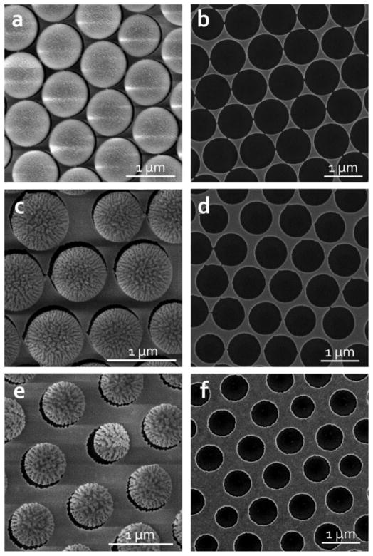
The first step in the fabrication procedure used nanosphere lithography to produce nanoholes in a gold film. The resulting arrays had long-range order on the length of centimeters with large grain sizes and minimal lattice defects. An oxygen-based RIE was used to reduce the diameter of the close-packed polystyrene nanospheres, introducing a tunable gap between the structures based on the duration of the etch. Fig. 2 demonstrates the variation in geometric parameters with etch time, roughly demonstrating a linear etch rate. The capacitively-coupled plasma, in addition to reducing the diameter of the polystyrene beads, also introduces surface roughness to the exposed bead surface that increases with increased etching time. The origin of the surface roughness remains unclear, although it has been proposed that it might originate from highly mobile surface monomers on the polystyrene surface [68]. Regardless of the mechanism, the roughness is highly repeatable and can be carefully controlled using the RIE etch parameters. In this experiment, the sharp nanoscale features associated with the polystyrene roughness were transferred to the circumference of the gold nanohole using a highly directional e-beam PVD deposition method (Fig. 2). These features can be seen in the nanohole patterns in Fig. 2, but are more evident as longitudinal features along the length of the pillars in Fig. 4. Despite the lack of an adhesion layer, omitted because of the gold’s role in the subsequent etch, the gold film maintained the sharp features from the polystyrene mask with excellent precision (Fig. 2b, 2d, and 2f).
Figure 2.
SEM images of PS arrays (coated with gold for imaging purposes) after O2 RIE for (a) 1 min, (c) 3 min, and (e) 5 min. (b), (d), and (f) are the corresponding gold nanohole arrays after removing the PS beads from (a), (c), and (e) respectively.
Figure 4.
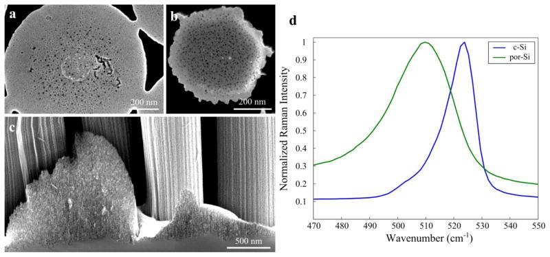
Contrast-enhanced SEM images of the porous silicon nanopillars: (a), (b) at the top surface of the pillars, and (c) along the length of the pillars. (d) Raman spectra of the LO phonon peak for both a crystalline silicon wafer and porous silicon nanopillar sample.
As seen in Fig. 2, the 2-D surface roughness of the etched polystyrene spheres is essentially projected onto the 2-D silicon surface to create the gold nanohole template with line-roughened edges. These features were maintained throughout the wet chemical etching of silicon due to the highly anisotropic nature of the etch in the (100) direction. The directionality of the etch was enhanced by using a very high etch parameter (ρ =0.97 where ρ =[HF]/([HF]+[H2O2]) to ensure that the etch process was limited by the rate of hole injection into the silicon. Minimizing hole diffusion away from the gold-Si interface is vital to confining the Si etch locally to the interface. The longitudinal grooves, produced from the line-edge roughness in the gold nanoholes, are on the order of 1–10 nm in size with little variation along the entire length of the pillar. In fact, these surface features demonstrate aspect ratios well over 2000 and can be tuned via the oxygen RIE in the polystyrene etch step.
To examine the collective effects of periodic silicon nanopillar arrays, the height and subsequently aspect ratio of the silicon nanopillars was controlled by varying the duration of the catalytic etch with constant nanopillar diameter. Figs. 3b, 3c, and 3d show pillars that were created by etching for 30, 60, and 90 min respectively. The corresponding pillar heights were approximately 1.60 μm, 3.69 μm, and 7.38 μm. And the corresponding aspect ratios were approximately 2, 5, and 10. The overall etch rate for these samples was between 50 and 90 nm/min, but was strongly dependent on the etch conditions, including the chemical composition of the etchant, temperature of the bath, development of gaseous byproducts, and substrate itself. The etch rates presented here are lower than some previously reported works, most likely due to the low H2O2 concentration limiting the process speed [32,66]. It is possible to drastically improve the aspect ratios of the structures simply by reducing the radius or increasing the etch time, however, high-aspect-ratio pillars are difficult to dry without introducing tip bundling at the tips.
Figure 3.
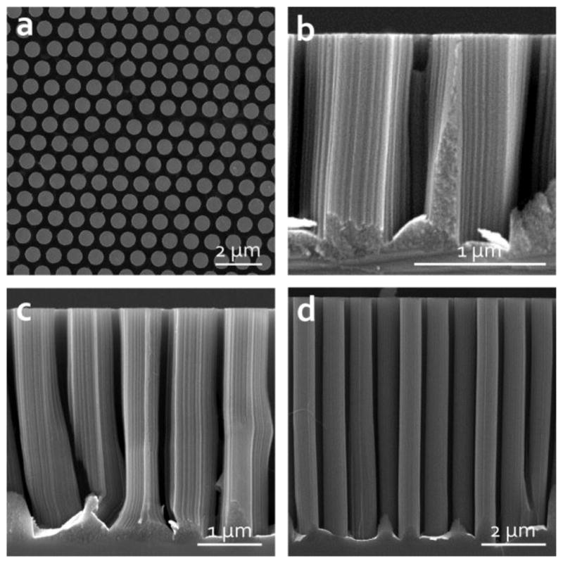
(a) Top-view SEM image of the nanopillar array to illustrate periodicity. Cross-sectional SEM images of the silicon nanopillars etched for (b) 30 min, (c) 60 min, and (d) 90 min.
The silicon nanopillar produced in this report also exhibit unique nanoscale porosity. The thickness of the overall pillar prohibits TEM characterization, but the pore-size appears to be on the order of single nanometers from the high-resolution SEM images (Fig. 4). Additionally, earlier studies have shown that porosity can be characterized by its effect on the energy of the longitudinal optical (LO) phonon in silicon [3]. Fig. 4d shows that the LO peak shifts to lower wavenumbers in the porous silicon nanopillar substrates when compared to the crystalline silicon (c-Si). The energetic shift of the LO peak has been attributed to phonon confinement in quasi-spherical nanocrystallites, and can be used to model the crystallite size. The silicon nanopillars in this experiment demonstrate a LO phonon peak at approximately 509 cm−1 and correspond to a nanocrystallite size of 2–3 nm [3]. These estimations agree well with the photoluminescence data described in later sections (Fig. 8).
Figure 8.
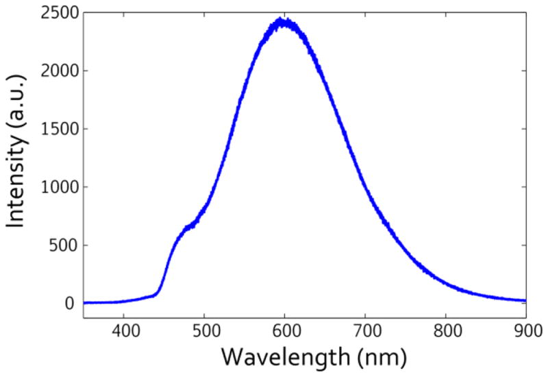
Photoluminescence spectra from the porous silicon nanopillar arrays excited using a 405 nm laser.
Nanoscale porosity in silicon has been reported in the catalytic etching of highly doped silicon substrates (0.01–0.001 Ωcm−1), under highly oxidizing chemical environments (ρ = 0.3), and in Ag-containing solutions. The previously proposed mechanisms for the non-local etching (i.e., etching at defect sites, hole diffusion, and ion diffusion) cannot satisfactorily explain the porosity developed in this work. Generally, defect sites on the silicon surface do provide favorable sites for etch nucleation, however, the lightly doped substrates in this experiment (10–100 Ωcm−1) have much lower defect concentrations than the substrates used in [44]. Additionally, control samples (i.e., clean silicon wafer) do not develop any porosity when subjected to the same etch conditions. Hole diffusion away from the catalytic interface has been demonstrated to cause porosity in Si in experiments where the etching regime is limited by the amount of corrosive element (HF) supplied to the surface, although the reported porosity does not closely resemble the nanoporous structure seen here [32]. Further control experiments with planar thin gold films indicate that the porosity is not confined to the immediate vicinity of the gold-Si interface, but extend up to millimeters away from it. Furthermore, the porosity is uniform regardless of its proximity to the catalytic interface, and should therefore not rely on the diffusion of holes away from the gold surface. Finally, gold has excellent chemical stability, which prevents the dissolution of the catalytic film into free Au+ ions in solution. The extremely high aspect ratios of the surface features also point to the fact that the integrity of the gold film was maintained throughout the etching process. While reasonable explanations have been proposed for the development of porosity in catalytic silicon etching under various conditions, they cannot fully explain the results from these experiments, suggesting that a different underlying mechanism is behind the porosity observed here. Further work needs to be done to fully elucidate the mechanism at work here, however, the presence of the gold and highly non-local nature of the porosity point to transport effects through the etchant solution at the silicon interface.
Antireflection Properties of Porous Silicon Nanopillar Arrays
Fig. 5 plots the absolute reflectance of three porous silicon nanopillar samples etched for 30, 60, and 90 min at both 10° and 45° incidence (θ) over the visible spectrum. The shape of the reflection curves is generally consistent with a polished silicon wafer, although a wafer generally has a reflectance of about 35% in the visible range and nearly 80% in the UV [69]. From Fig. 5, the porous silicon nanopillar structures reduce the reflectance approximately twofold (30 min etch) or nearly fivefold (60/90 min etches) compared to the polished silicon, with the longer pillars generally exhibiting reflectance below 10% in the visible/NIR range. The porous silicon nanopillar geometry used in this work is not optimized for reflection reduction and could be improved by optimizing the aspect ratio and period. Fig. 5 also indicates that the nanostructured substrates effectively reduce reflection for a broad range of incidence angles, shown through the reflectance curves at both 10° and 45° incidence (θ). The reduced reflection is consistent with previous reports on structured silicon arrays and indicates that the porosity does not diminish the ensemble properties of the porous silicon nanopillar arrays [70,71].
Figure 5.
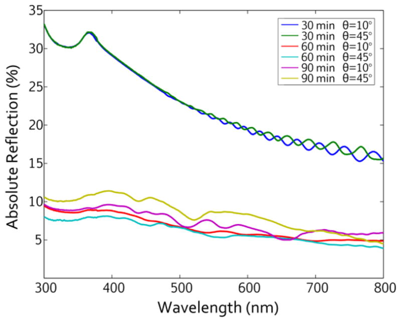
Absolute Reflectance from the porous silicon nanopillar arrays with various etch times (30, 60, 90 min) and incidence angles (10° and 45°).
Superhydrophobicity Properties of Porous Silicon Nanopillar Arrays
Fig. 6a plots the contact angle of a water droplet on substrates with various pillar heights, including an angle of 94° for the water on a flat Si substrate. The images in Fig. 6b, 6c, and 6d are taken for the porous silicon nanopillar samples etched for 30, 60, and 90 min. Our results show that increasing the height of the nanostructures causes the water contact angle to increase, up to nearly 140° in this case—this observation is consistent with other reported works [72,73]. To qualitatively explain the wetting behavior, we fit the data with Cassie and Baxter’s model. Comparing the model to a fit of our data, we were able to extract approximate values of the areal fraction of the liquid-solid interface (red curve in Fig. 6a).
Figure 6.
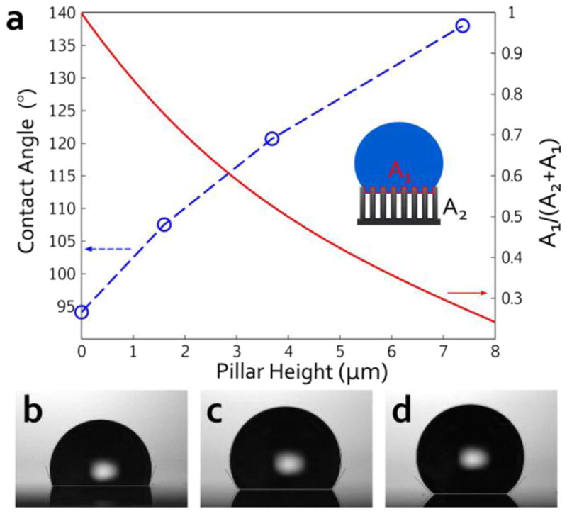
(a) Plot of contact angle (left axis) and areal fraction of liquid-solid interface (right axis) vs. silicon nanopillar height. Contact angle images of water droplets on the silicon nanopillar samples with various etch times: (b) 30 min, (c) 60 min, and (d) 90 min.
The results indicate that increasing the pillar height simply increases the amount of air that is trapped underneath the liquid, and only small portions at the top of the nanopillars are exposed to the liquid. The minimal surface area in contact with the liquid could be invaluable for a variety of biosensing and lab-on-a-chip applications.[74–80] As before, the porous silicon nanopillar arrays developed in this work were not optimized for applications in hydrophobicity and can be further improved by tuning the geometric parameters of the arrays.
SERS Properties of Porous Silicon Nanopillar Arrays
In order to use the porous silicon nanopillar arrays for SERS substrates, metal deposition onto the porous silicon nanopillar surfaces was accomplished via two mechanisms: electrochemical plating and sputtering. These two methods were utilized in an attempt to deposit a conformal film onto the surface of the pillars to utilize their nanoscale features for large volumes of electromagnetic field enhancement.
In the first approach (i.e., electrochemical deposition of Ag), the pillars served as nucleation points for metal particle growth. As growth proceeded, the isolated Ag particles made connections to form a mesoscale Ag network. Characterization indicates that the Ag growth can occur between the silicon nanopillar below the surface of the original substrate, although it is much less common. Precise control of the growth conditions was required to prevent the formation of a continuous Ag film. The second attempt to deposit a thin metal film on the pillar surfaces utilized a thin film sputter coater to coat the substrates with Au. The deposition resulted in a continuous gold film only at the top surface of the silicon nanopillars. A subsequent treatment at 500 °C helped redistribute some of the metal to the nanopillar sidewalls. The resulting morphology is that of a continuous film on the top surfaces of the pillars with a discontinuous nanoscale network of Au particles covering the nanopillar sidewalls. Our results indicate that the silicon nanopillar arrays can perform as excellent SERS substrates and potentially be improved by reducing the nanopillar diameters on the order of 100 nm for stronger plasmonic enhancement.
To examine the SERS performance, we used a popular chemical dye – Rhodamine 6G, because of its well documented Raman transitions. A representative SERS spectrum from the Rhodamine 6G on the Ag-coated silicon nanopillar substrates incubated in R6G is shown in Fig. 7. We note that the prominent peaks at 1651, 1576, 1510, 1362, 1127, 775, and 614 cm−1 are all consistent with literature on the Raman transitions of the Rhodamine 6G molecule [81–83]. We also note that the smaller peaks at 1190, 1305, and 1410 cm−1 can potentially be attributed to unreacted agents or byproducts left behind from the solution-phase electrochemical deposition. The spectrum is given from the Ag-coated substrates because they resulted in a stronger SERS response from the Rhodamine 6G. The strong SERS spectra in Fig. 7 indicates that these substrates can be used for sensitive SERS detection, as the Rhodamine 6G Raman signal on a bare silicon wafer cannot be detected at all with the same setup.
Figure 7.
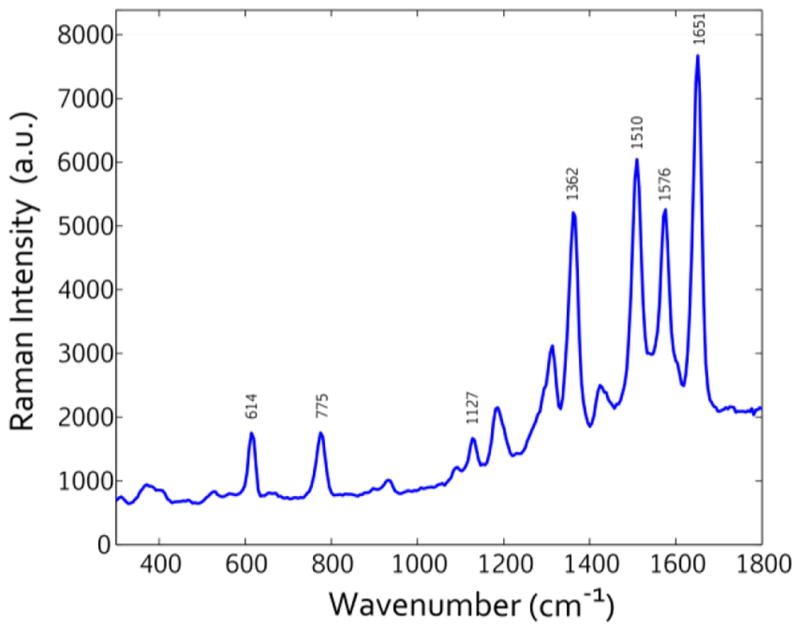
SERS data from electrochemically-deposited silver silicon nanopillar substrates incubated in R6G.
Photoluminescence Properties of Silicon Nanopillar Arrays
Finally, photoluminescence from the nanopillar structures was examined using a laser excitation at 405 nm. The 3 mW laser was coupled through an attenuator and microscope before being filtered out of the collection beam. We noted that the relatively high laser power (mW range) generally caused beam-induced morphology changes localized to the focused laser spot and subsequently utilized the attenuator to diminish these fairly common effects. A representative spectra is given in Fig. 8, with a clear emission band at 600 nm, a peak generally attributed to quantum confinement in the nanocrystallite that agrees well with the 2–3 nm sizes of the Si nanocrystallites estimated from the LO phonon peak shift in the Raman scattering data [84]. A smaller peak at 480 nm is also visible as a shoulder to the 600 nm peak; this peak can be attributed to either luminescence from 2.0 nm crystallites [85,86] or surface recombination states on the Si surface related to oxide defect states or hydroxyl conjugated terminations [87,88]. The photoluminescence emission is consistent across all porous control and nanopillar samples, indicating highly uniform crystallite size.
4. Conclusion
We have demonstrated the fabrication of highly-periodic, well-aligned, porous silicon nanopillar arrays using a metal-catalyzed etch of a (100) Si substrate. The resulting pillars retain nanometer scale features from the template, including grooves along their length that could have significant impacts for SERS sensing. The pillars also have a nanoporous structure that could lead to important applications in batteries and energy storage. Reflection and wetting data show that the porous silicon nanopillar substrates strongly reduce the reflection from the Si surface and discourage the wetting of water-based solutions. To demonstrate the multi-functionality of a single sample, all of the tests were performed on the same porous silicon nanopillar substrate, but the parameters of the silicon nanopillars can certainly be optimized for each property. Finally, the same sample was used in the electrochemical deposition of Ag and served as nucleation sites for Ag nanoparticle growth to demonstrate the ability to be highly sensitive SERS substrate.
The multifunctional nature of the porous silicon nanopillar substrates could play an important role in their future development as optical and electrical sensors, energy storage and harvesting units, electronic biological interfaces, and electronic and photonic materials. For example, the fluidic confinement demonstrated in this work could be used to deliver highly dilute analytes to a very small volume at the top of the porous silicon nanopillar arrays, enabling highly sensitive optical detection schemes. Furthermore, the nanoscale porosity could enable highly sensitive optical and electronic sensors, in addition to efficient Si anodes in the development of Li-ion batteries. Finally, the combination of microscale and nanoscale features could provide important electronic interfaces in biology, and photonic materials with unique dispersive properties.
Acknowledgments
This research was supported by National Institutes of Health (NIH) Director’s New Innovator Award (1DP2OD007209-01), National Science Foundation (NSF), National Science Foundation Graduate Research Fellowship (Grant No. DGE-0750756), and the Penn State Center for Nanoscale Science (MRSEC) under grant DMR-0820404. Components of this work were conducted at the Penn State node of the NSF-funded National Nanotechnology Infrastructure Network.
References
- 1.Wolkin MV, Jorne J, Fauchet PM, Allan G, Delerue C. Phys Rev Lett. 1999;82:197. [Google Scholar]
- 2.Koenigsmann C, Sutter E, Adzic RR, Wong SS. J Phys Chem C. 2012;116:15297. [Google Scholar]
- 3.Zheng YB, Huang TJ, Desai AY, Wang SJ, Tan LK, Gao H, Huan ACH. Appl Phys Lett. 2007;90:183117. [Google Scholar]
- 4.Hu L, Wu H, Gao Y, Cao A, Li H, McDough J, Xie X, Zhou M, Cui Y. Adv Energy Mater. 2011;1:523. [Google Scholar]
- 5.Ye T, Kumar AS, Saha S, Takami T, Huang TJ, Stoddart JF, Weiss PS. ACS Nano. 2010;4:3697. doi: 10.1021/nn100545r. [DOI] [PubMed] [Google Scholar]
- 6.Law M, Goldberger J, Yang P. Annu Rev Mater Sci. 2004;34:83. [Google Scholar]
- 7.Chaki NK, Mandal S, Reber AC, Qian M, Saavedra HM, Weiss PS, Khanna SN, Sen A. ACS Nano. 2010;4:5813. doi: 10.1021/nn101640r. [DOI] [PubMed] [Google Scholar]
- 8.Yao D, Zhang G, Li B. Nano lett. 2008;8:4557. doi: 10.1021/nl802807t. [DOI] [PubMed] [Google Scholar]
- 9.Liu YJ, Hao QZ, Smalley JST, Liou J, Khoo IC, Huang TJ. Appl Phys Lett. 2010;97:091101. [Google Scholar]
- 11.Kang Z, Liu Y, Lee S-T. Nanoscale. 2011;3:777. doi: 10.1039/c0nr00559b. [DOI] [PubMed] [Google Scholar]
- 12.Angelis FD, Gentile F, Mecarini F, Das G, Moretti M, Candeloro P, Coluccio ML, Cojoc G, Accardo A, Liberale C, Zaccaria RP, Perozziello G, Tirinato L, Toma A, Cuda G, Cingolani R, Fabrizio ED. Nat Photonics. 2011;5:2. [Google Scholar]
- 13.Cullis A, Canham LT. Nature. 1991;353:335. [Google Scholar]
- 14.Delerue C, Allan G. Phys Rev B. 1993;48:24. doi: 10.1103/physrevb.48.11024. [DOI] [PubMed] [Google Scholar]
- 15.Nassiopoulos AG, Grigoropoulos S, Papadimitriou D. Appl Phys Lett. 1996;69:2267. [Google Scholar]
- 16.Malinin A, Ovchinnikov V, Novikov S, Tuovinen C, Hovinen A. Mater Sci Eng, B. 2000;74:32. [Google Scholar]
- 17.Cloutier SG, Hsu C-H, Kossyrev PA, Xu J. Adv Mater. 2006;18:841. [Google Scholar]
- 18.Walavalkar SS, Hofmann CE, Homyk AP, Henry MD, Atwater HA, Scherer A. Nano lett. 2010;10:4423. doi: 10.1021/nl102140k. [DOI] [PubMed] [Google Scholar]
- 19.Chern W, Hsu K, Chun IS, de Azeredo BP, Ahmed N, Kim K-H, Zuo J-M, Fang N, Ferreira P, Li X. Nano lett. 2010;10:1582. doi: 10.1021/nl903841a. [DOI] [PubMed] [Google Scholar]
- 20.Tang J, Wang H-T, Lee DH, Fardy M, Huo Z, Russell TP, Yang P. Nano lett. 2010;10:4279. doi: 10.1021/nl102931z. [DOI] [PubMed] [Google Scholar]
- 21.Boukai AI, Bunimovich Y, Tahir-Kheli J, Yu J-K, Goddard Wa, Heath JR. Nature. 2008;451:168. doi: 10.1038/nature06458. [DOI] [PubMed] [Google Scholar]
- 22.Payton OD, Picco L, Robert D, Raman A, Homer ME, Champneys AR, Miles MJ. Nanotechnology. 2012;23:205704. doi: 10.1088/0957-4484/23/20/205704. [DOI] [PubMed] [Google Scholar]
- 23.Juluri BK, Zheng YB, Ahmed D, Jensen L, Huang TJ. J Phys Chem C. 2008;112:7309. [Google Scholar]
- 24.Vaish A, Liao WS, Shuster MJ, Hinds JM, Weiss PS, Andrews AM. Anal Chem. 2011;83:7451. doi: 10.1021/ac2016536. [DOI] [PubMed] [Google Scholar]
- 25.Claridge SA, Castleman AW, Khanna JS, Murray CB, Sen A, Weiss PS. ACS Nano. 2009;3:244. doi: 10.1021/nn800820e. [DOI] [PubMed] [Google Scholar]
- 26.Huang TJ, Liu M, Knight LD, Grody WW, Miller JF, Ho CM. Nucleic Acids Res. 2002;30:e55. doi: 10.1093/nar/gnf054. [DOI] [PMC free article] [PubMed] [Google Scholar]
- 27.Zheng YB, Kiraly B, Weiss PS, Huang TJ. Nanomedicine. 2012;7:751. doi: 10.2217/nnm.12.30. [DOI] [PMC free article] [PubMed] [Google Scholar]
- 28.Zhao YH, Lin SS, Nawaz AA, Kiraly B, Hao QZ, Liu YJ, Huang TJ. Optics Express. 2010;18:23458. doi: 10.1364/OE.18.023458. [DOI] [PubMed] [Google Scholar]
- 29.Yang S, Guo F, Kiraly B, Mao X, Lu M, Leong KW, Huang TJ. Lab Chip. 2012;12:2097. doi: 10.1039/c2lc90046g. [DOI] [PMC free article] [PubMed] [Google Scholar]
- 30.Zhang BX, Zhao YH, Hao QZ, Kiraly B, Khoo IC, Chen SF, Huang TJ. Optics Express. 2011;19:15221. doi: 10.1364/OE.19.015221. [DOI] [PubMed] [Google Scholar]
- 31.Beale MIJ, Benjamin JD, Uren MJ, Chew NG, Cullis AG. J Cryst Growth. 1985;73:622. [Google Scholar]
- 32.Li X, Bohn PW. Appl Phys Lett. 2000;77:2572. [Google Scholar]
- 33.Cruz S, Hönig-d’ Orville A, Müller J Electrochem Soc. 2005;152:C418. [Google Scholar]
- 34.Peng K, Fang H, Hu J, Wu Y, Zhu J, Yan Y, Lee S. Chemistry. 2006;12:7942. doi: 10.1002/chem.200600032. [DOI] [PubMed] [Google Scholar]
- 35.Xia X, Ashruf C, French P, Kelly J. Chem Mater. 2000;12:1671. [Google Scholar]
- 36.Peng K, Wu Y, Fang H, Zhong X, Xu Y, Zhu J. Angew Chem Int Ed. 2005;44:2737. doi: 10.1002/anie.200462995. [DOI] [PubMed] [Google Scholar]
- 37.Choi WK, Liew TH, Dawood MK, Smith HI, Thompson CV, Hong MH. Nano lett. 2008;8:3799. doi: 10.1021/nl802129f. [DOI] [PubMed] [Google Scholar]
- 38.Huang Z, Shimizu T, Senz S, Zhang Z, Zhang X, Lee W, Geyer N, Gösele U. Nano Lett. 2009;9:2519. doi: 10.1021/nl803558n. [DOI] [PubMed] [Google Scholar]
- 39.Guichard AR, Barsic DN, Sharma S, Kamins TI, Brongersma ML. Nano Lett. 2006;6:2140. doi: 10.1021/nl061287m. [DOI] [PubMed] [Google Scholar]
- 40.Wang R-C, Chao C-Y, Su W-S. Acta Mater. 2012;60:2097. [Google Scholar]
- 41.Peng K-Q, Wang X, Lee S-T. Appl Phys Lett. 2009;95:243112. [Google Scholar]
- 42.Chen H, Zou R, Chen H, Wang N, Sun Y, Tian Q, Wu J, Chen Z, Hu J. J Mater Chem. 2011;21:801. [Google Scholar]
- 43.Qu Y, Zhong X, Li Y, Liao L, Huang Y, Duan X. J Mater Chem. 2010;20:3590. doi: 10.1039/c0jm00493f. [DOI] [PMC free article] [PubMed] [Google Scholar]
- 44.Xie YL, Zhao CL, Zhao YH, Li SX, Rufo J, Yang SK, Guo F, Huang TJ. Lab Chip. 2013;13:1772. doi: 10.1039/c3lc00043e. [DOI] [PMC free article] [PubMed] [Google Scholar]
- 45.Hwang HH, Meyyappan M, Mathad GS, Ranade R. J Vac Sci Technol. 2002;20:2199. [Google Scholar]
- 46.Lin L, Sun X, Tao R, Feng J, Zhang Z. Nanotechnology. 2011;22:075203. doi: 10.1088/0957-4484/22/7/075203. [DOI] [PubMed] [Google Scholar]
- 47.Qu Y, Zhou H, Duan X. Nanoscale. 2011;3:4060. doi: 10.1039/c1nr10668f. [DOI] [PMC free article] [PubMed] [Google Scholar]
- 48.Xie YL, Ahmed D, Lapsley MI, Lin SCS, Nawaz AA, Wang L, Huang TJ. Anal Chem. 2012;84:7495. doi: 10.1021/ac301590y. [DOI] [PMC free article] [PubMed] [Google Scholar]
- 49.Liu YM, Zhang X. Nanoscale. 2012;4:5277. doi: 10.1039/c2nr31140b. [DOI] [PubMed] [Google Scholar]
- 50.Yoon S-S, Khang D-Y. J Mater Chem. 2012;22:10625. [Google Scholar]
- 51.Yang S, Guo F, Kiraly B, Mao X, Lu M, Leong KW, Huang TJ. Lab chip. 2012;12:2097. doi: 10.1039/c2lc90046g. [DOI] [PMC free article] [PubMed] [Google Scholar]
- 52.Liu YM, Palomba S, Park Y, Zentgraf T, Yin XB, Zhang X. Nano Lett. 2012;12:4853. doi: 10.1021/nl302339z. [DOI] [PubMed] [Google Scholar]
- 53.Zheng Y, Kiraly B, Huang TJ. Nanomedicine. 2010;5:1309. doi: 10.2217/nnm.10.111. [DOI] [PubMed] [Google Scholar]
- 54.Heo C-J, Jeon HC, Lee SY, Jang SG, Cho S, Choi Y, Yang S-M. J Mater Chem. 2012;22:13903. [Google Scholar]
- 55.He L, Huang J, Xu T, Chen L, Zhang K, Han S, He Y, Lee ST. J Mater Chem. 2012;22:1370. [Google Scholar]
- 56.Haes AJ, Van Duyne RP. J Am Chem Soc. 2002;124:10596. doi: 10.1021/ja020393x. [DOI] [PubMed] [Google Scholar]
- 57.Haes AJ, Chang L, Klein WL, Van Duyne RP. J Am Chem Soc. 2005;127:2264. doi: 10.1021/ja044087q. [DOI] [PubMed] [Google Scholar]
- 58.Li Y, Koshizaki N, Cai W. Coord Chem Rev. 2011;255:357. [Google Scholar]
- 59.Li Y, Cai W, Duan G. Chem Mater. 2007;20:615. [Google Scholar]
- 60.Yang S, Lei Y. Nanoscale. 2011;3:2768. doi: 10.1039/c1nr10296f. [DOI] [PubMed] [Google Scholar]
- 61.Lei Y, Yang S, Wu M, Wilde G. Chem Soc Rev. 2011;40:1247. doi: 10.1039/b924854b. [DOI] [PubMed] [Google Scholar]
- 62.Kosiorek A, Kandulski W, Glaczynska H, Giersig M. Small. 2005;1:439. doi: 10.1002/smll.200400099. [DOI] [PubMed] [Google Scholar]
- 63.Gwinner MC, Koroknay E, Fu L, Patoka P, Kandulski W, Giersig M, Giessen H. Small. 2009;5:400. doi: 10.1002/smll.200800923. [DOI] [PubMed] [Google Scholar]
- 64.Vogel N, Fischer J, Mohammadi R, Retsch M, Butt H-J, Landfester K, Weiss CK, Kreiter M. Nano Lett. 2011;11:446. doi: 10.1021/nl103120s. [DOI] [PubMed] [Google Scholar]
- 65.Fischer J, Vogel N, Mohammadi R, Butt H-J, Landfester K, Weiss CK, Kreiter M. Nanoscale. 2011;3:4788. doi: 10.1039/c1nr10952a. [DOI] [PubMed] [Google Scholar]
- 66.Yao Y, McDowell MT, Ryu I, Wu H, Liu N, Hu L, Nix WD, Cui Y. Nano Lett. 2011;11:2949. doi: 10.1021/nl201470j. [DOI] [PubMed] [Google Scholar]
- 67.Hong G, Li C, Qi L. Adv Funct Mater. 2010;20:3774. [Google Scholar]
- 68.Drotar JT, Zhao Y-P, Lu T-M, Wang G-C. Phys Rev B. 2000;62:2118. [Google Scholar]
- 69.Chao Y-C, Chen C-Y, Lin C-A, He J-H. Energy & Environmental Science. 2011;4:3436. [Google Scholar]
- 70.Diedenhofen SL, Vecchi G, Algra RE, Hartsuiker A, Muskens OL, Immink G, Bakkers EPAM, Vos WL, Rivas JG. Adv Mater. 2009;21:973. [Google Scholar]
- 71.Yao Y, Yao J, Narasimhan VK, Ruan Z, Xie C, Fan S, Cui Y. Nat Commun. 2012;482:278. doi: 10.1038/ncomms1664. [DOI] [PubMed] [Google Scholar]
- 72.Shiu J, Kuo C, Chen P. Chem Mater. 2004;16:561. [Google Scholar]
- 73.Lai KY, Lin Y-R, Wang H-P, He J-H. CrystEngComm. 2011;13:1014. [Google Scholar]
- 74.Neuzil P, Giselbrecht S, Lange K, Huang TJ, Manz A. Nat Rev Drug Discovery. 2012;11:620. doi: 10.1038/nrd3799. [DOI] [PMC free article] [PubMed] [Google Scholar]
- 75.Zhao YH, Stratton ZS, Guo F, Lapsley MI, Chan CY, Lin SCS, Huang TJ. Lab Chip. 2013;13:17. doi: 10.1039/c2lc90127g. [DOI] [PMC free article] [PubMed] [Google Scholar]
- 76.Mao XL, Huang TJ. Lab Chip. 2012;12:4006. doi: 10.1039/c2lc90100e. [DOI] [PMC free article] [PubMed] [Google Scholar]
- 77.Mao XL, Huang TJ. Lab Chip. 2012;12:1412. doi: 10.1039/c2lc90022j. [DOI] [PMC free article] [PubMed] [Google Scholar]
- 78.Nawaz AA, Mao XL, Stratton ZS, Huang TJ. Lab Chip. 2013;13:1457. doi: 10.1039/c3lc90023a. [DOI] [PMC free article] [PubMed] [Google Scholar]
- 79.Li P, Stratton ZS, Dao M, Ritz J, Huang TJ. Lab Chip. 2013;13:602. doi: 10.1039/c2lc90148j. [DOI] [PMC free article] [PubMed] [Google Scholar]
- 80.Mao XL, Juluri BK, Lapsley MI, Stratton ZS, Huang TJ. Microfluid Nanofluid. 2010;8:139. [Google Scholar]
- 81.Yang S, Cai W, Kong L, Lei Y. Adv Funct Mater. 2010;20:2527. [Google Scholar]
- 82.Yang S, Lapsley MI, Cao B, Zhao C, Zhao Y, Hao Q, Kiraly B, Scott J, Li W, Wang L, Lei Y, Huang TJ. Adv Funct Mater. 2013;23:720. doi: 10.1002/adfm.201201466. [DOI] [PMC free article] [PubMed] [Google Scholar]
- 83.Yang S, Xu F, Ostendorp S, Wilde G, Zhao H, Lei Y. Adv Funct Mater. 2011;21:2446. [Google Scholar]
- 84.Yang S, Cai W, Zeng H, Li Z. J Appl Phys. 2008;104:23516o. [Google Scholar]
- 85.Delerue C, Allan G, Lannoo M. Phys Rev B. 1993;48:11024. doi: 10.1103/physrevb.48.11024. [DOI] [PubMed] [Google Scholar]
- 86.Serdiuk T, Lysenko V, Alekseev S, Skryshevsky VA. J Colloid Interface Sci. 2011;364:65. doi: 10.1016/j.jcis.2011.07.068. [DOI] [PubMed] [Google Scholar]
- 87.Yang S, Kiraly B, Wang WY, Shang SL, Cao B, Zeng H, Zhao Y, Li W, Liu Z-K, Cai W, Huang TJ. Adv Mater. 2012;24:5598. doi: 10.1002/adma.201202286. [DOI] [PMC free article] [PubMed] [Google Scholar]
- 88.Yang S, Li W, Cao B, Zeng H, Cai W. J Phys Chem C. 2011;115:21056. [Google Scholar]


