Abstract
The recently developed alumina and Parylene C bi-layer encapsulation improved the lifetime of neural interfaces. Tip deinsulation of Utah electrode array based neural interfaces is challenging due to the complex 3D geometries and high aspect ratios of the devices. A three-step self-aligned process was developed for tip deinsulation of bilayer encapsulated arrays. The deinsulation process utilizes laser ablation to remove Parylene C, O2 reactive ion etching to remove carbon and Parylene residues, and buffered oxide etch to remove alumina deposited by atomic layer deposition, and expose the IrOx tip metallization. The deinsulated iridium oxide area was characterized by scanning electron microscopy, atomic force microscopy, X-ray photoelectron spectroscopy, and electrochemical impedance spectroscopy to determine the morphology, surface morphology, composition, and electrical properties of the deposited layers and deinsulated tips. The alumina layer was found to prevent the formation of micro cracks on iridium oxide during the laser ablation process, which has been previously reported as a challenge for laser deinsulation of Parylene films. The charge injection capacity, charge storage capacity, and impedance of deinsulated iridium oxide were characterized to determine the deinsulation efficacy compared to Parylene-only insulation. Deinsulated iridium oxide with bilayer encapsulation had higher charge injection capacity (240 vs 320 nC) and similar electrochemical impedance (2.5 vs 2.5 kΩ) compared to deinsulated iridium oxide with only Parylene coating for an area of 2 × 10⁻⁴ cm2. Tip impedances were in the ranges of 20 to 50 kΩ, with median of 32 KΩ and standard deviation of 30 kΩ, showing the effectiveness of the self-aligned deinsulation process for alumina and Parylene C bi-layer encapsulation. The relatively uniform tip impedance values demonstrated the consistency of tip exposures.
2 Introduction
Neural interfaces have been developed for therapies applied to neural disorders and diseases [1–4], and in the pursuit of basic neuroscience research. Implanted neural interfaces have a range of invasiveness and for some applications require chronic implantation, and therefore exposed to physiological fluids for long periods. The long-term exposure of devices to the physiological environment requires high-performance encapsulation, particularly as integration of active electronics on the devices become more common. Hermetic enclosures and polymer encapsulation (bulk and thin-film) are the dominant techniques. Encapsulation has been preferred for neural interfaces due to many feedthroughs and volume limitations. Parylene C has been widely used as a encapsulation materials for biomedical implantable devices [5–9] because of its chemical inertness, low dielectric constant (εr=3.15) [10], low water vapor transmission rate (WVTR) of 0.2 g·mm/m2·day [11], high resistivity (~ 1015 Ω·cm), and USP class VI biocompatibility [12]. Parylene C is also an excellent ion barrier [13], which is very important for implants exposed to physiological environment to avoid nucleation of liquid water, electrical shorts, and accelerated electrochemical corrosion and degradation. Failures of Parylene coating have been reported [14] because of moisture penetration, interface contamination, and cracking of the material[15]. We have previously reported that atomic layer deposited (ALD) alumina and Parylene C (A+P) bilayer encapsulation can be an effective encapsulation strategy to prevent the moisture ingress and separate moisture from interface contaminants[16–18]. In this paper, we report a highly effective self-aligned and maskless process to deinsulate the electrode tips of bilayer encapsulated Utah Electrode Arrays (UEAs).
Both ALD and Gorham process for depositing alumina and Parylene C, repesctively, generate extremely conformal films due to the nature of the surface reaction that generates the films [10]. This results in high insulation impedance to the physiological environment due to the high resistivity of these dielectric materials, and the pin-hole free character of the films. However, neural recording and stimulation require information exchange between the neural interface and the adjacent neurons. Selective removal of alumina and Parylene C from the electrode tips is required to generate active recording and stimulation sites for the device [19]. Wet etching is not a viable option for Parylene C since it is inert to most solvents. Historically, tip deinsulation of microelectrodes used high temperatures to burn off the insulation or high-voltage discharge to ablate the insulation [20]. The heating method has been reported to cause damage and degradation to the insulation near the tip and also damage the active electronics. The high-voltage arc based deinsulation technique led to fractures in the Parylene insulation along the electrodes[20], and is also likely not possible with devices that include integrated electronics if required after integration of the components. Also, it was difficult for those methods to accurately control the tip exposure, which is a critical factor in the impedance and selectivity of the electrodes. Several dry etching methods have been investigated, including plasma etching, reactive ion etching (RIE), and deep reactive ion etching (DRIE) [5, 21].
Oxygen plasma etching has been used as a standard Parylene C etching process for UEAs for more than a decade [5]. Due to its complex 3D geometries, precise masking for the electrode tips is a challenge. Both Photoresist and aluminum foil have been used as masks for oxygen plasma etching during UEA manufacturing [22–24]. Use of Photoresist is not applicable to individual UEAs, therefore poking the UEA through a thin aluminum foil to expose the tips is the current process. The major drawback with aluminum foil masking is the low precision and accuracy of the tip exposure control, resulting significant variations in tip impedance and selectivity. Also the poking process is labor intensive and decreases yield through mechanical damage and fractures to the electrode tips. Our group and others have previously reported that laser ablation of Parylene C can be effective and adaptable method to remove Parylene encapsulation [25–29].
The alumina film at the tip of UEA also needs to be removed to obtain the desired electrochemical characteristics of iridium oxide for neural recording/stimulation. Plasma etching has been widely used for etching of Al2O3 [30, 31]. The etching rate was about 1 nm/minutes with RF power of 100 W[32], which is a slow process for a 50 nm thick alumina layer. Alternative wet etching method needs to be adopted to remove alumina. Due to the incorporation of hydrogen in the form of OH groups in the film [33, 34], liquid water is known to slowly corrode ALD Al2O3 thin films [35]. Given the known dissolution of alumina in liquid water and extreme inertness of Parylene C in wet etching, buffered oxide etch (BOE, 6:1 volume ratio of 40% NH4F in water to 49% HF in water) wet etching can be used to remove alumina by utilizing Parylene C as a mask layer.
Compared with traditional deinsulation methods like heat ablation or reactive ion etching for micro-machined biosensors and biomedical devices, the method reported here, combining laser ablation, oxygen plasma and BOE etching, is a self-aligned process and completely eliminates the need of masks. This self-aligned process is extremely beneficial for biomedical devices with complex geometries, which otherwise requires challenging 3-D micromachining. Additionally, this method has better control of the etching area, leading to better uniformity, reproducibility, and performance.
Charge injection capacity (CIC), charge storage capacity (CSC), and electrochemical impedance are critical for neural stimulation/recording. The CIC, CSC, and electrochemical impedance of deinsulated iridium oxide were characterized by chronopotentiometry, cyclic voltammetry (CV), and electrochemical impedance spectroscopy (EIS), respectively. The electrochemical properties of deinsulated iridium oxide with bilayer encapsulation were found to be stable and similar to that of iridium oxide with Parylene C only coating. Analytical techniques were used to optimize the deinsulation quality.
3 Materials and Methods
3.1 Deinsulation Process for Alumina and Parylene Coating
A three-step process was investigated to deinsulate the A+P bilayer encapsulation from active sputtered iridium oxide film (SIROF) electrode sites. Parylene-only test structures were also deinsulated as control samples. First, KrF excimer laser ablation (248 nm) Optec Micromaster was used to remove Parylene C. A detailed description of excimer deinsulation is reported elsewhere [29, 36]. Fluence and number of pulse during laser ablation are the two variables optimizing the deinsulation process. SIROF test structures were deinsulated by using 100 laser pulses with fluence of 1500 mJ/cm2 with pulse duration of 5 ns and frequency of 100 Hz, adopted from Yoo et al. [29].
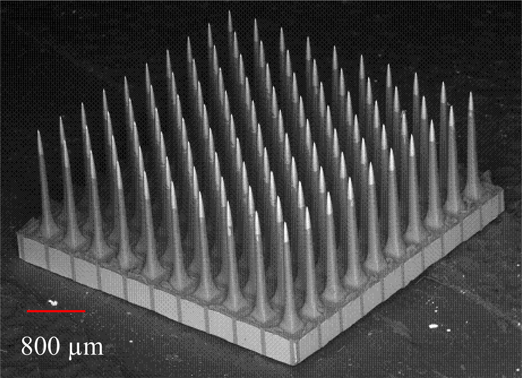
Laser ablation of Parylene C results in redeposition of carbon residue on and around the ablation site. In addition, residual Parylene might be present on the SIROF surface due to roughness, and the variability of incidence angles imposed by the UEA tip geometry, as show in Fig 1. A 2-minute oxygen plasma was used to remove the carbon contamination to improve the electrochemical impedance (Z (Ω)) and CIC (mC/cm2) of SIROF. The oxygen plasma etching used an inductively coupled plasma (ICP) based March Plasmod (March Plasma Systems), with RF power (13.56 MHz) of 150 W and chamber pressure of 400 mTorr. No mask was required for the oxygen plasma etching since it only etches about 500 nm of Parylene C.
Figure 1.
Back scattered scanning electron micrograph of the UEA with 100 (10 by 10) silicon electrodes. The electrode length is 1.5 mm and space between electrodes is 400 µm.
The third step in the process is the removal of alumina film to expose the active tip metal (iridium oxide). An 8-minute BOE etch at room temperature was used to remove alumina on the laser-ablated spots. Again, the Parylene acted as a mask for the BOE etch due to its chemical inertness. Alumina was etched only in the area where Parylene was removed by laser ablation. The BOE etch was found not to affect the electrochemical properties of the iridium oxide.
3.2 Fabrication of SIROF Test Structures and UEAs
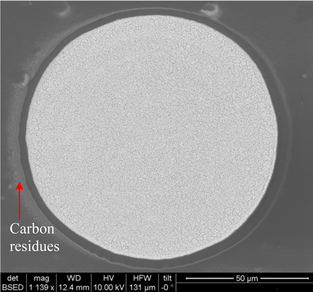
The characterization of this three-step self-aligned deinsulation process was first performed on SIROF planar test structures to allow high accuracy electrochemical impedance spectroscopy measurements due to precise deinsulation geometries (areas) and the simpler planar electrode arrangement. The deposition processes for metal, metal oxide, alumina, and Parylene C on planar test structures are described elsewhere [16, 22, 37, 38]. The test structures were fabricated on a 4 inch Si wafers. 600 nm of silicon nitride was deposited by LPCVD using NH3 and SiCl2H2 at a temperature 825 °C as an insulation layer between the substrate and the subsequent metal traces. A 50 nm titanium film was deposited followed by 200 nm platinum film by DC sputter deposition in Ar ambient (flow rate of 150 sccm) at 10 mTorr with sputtering power of 90 W (T–M Vacuum Super series). The titanium is an adhesion layer and the platinum is the primary trace metalization. The Sputtered Iridium Oxide Film (SIROF) was actively sputtered at a pressure of 10 mTorr with power of 100 W in Ar (flow rate of 100 sccm) and O2 (flow rate of 100 sccm) plasma. Lift-off process was used to pattern the SIROF. SIROF is the active tip metal for UEA electrodes [39]. The test structures were then annealed at 375 °C in Forming gas (Ar: H2 98%: 2%) for 45 minutes in a Linberg furnace. 52 nm of Al2O3 was deposited by plasma assisted atomic layer deposition (PAALD) using trimethylaluminum (TMA) and O2 plasma as precursors at a substrate temperature of 120 °C using a Cambridge Nanotech Fiji 200 ALD reactor. Details of the alumina deposition can be found at [16, 38, 40]. Silane A-174 (Momentive Performance Materials) was used to improve the adhesion between Al2O3 and Parylene C layer. A 6 μm Parylene C film was deposited using the Gorham process [10] in a LabTop 3000 Parylene coater (Para Tech Coating), using DPX-C dimer (Specialty Coating Systems). Silane A-174 (Momentive Performance Materials) was used to improve the adhesion between Al2O3 and Parylene C layer. Fig 2 is a SEM picture of a test structure after three-step deinsulation.
Figure 2.
Back-scattered SEM picture of a test structure after three-step deinsulation: laser ablation, oxygen plasma etching and BOE etch. Carbon residues were observed around the deinsulated SIROF spot.
The characterized three-step deinsulation process was applied to deinsulated bilayer encapsulated UEA electrodes. UEA was first designed and fabricated by Normann for intracortical stimulation [22]. A dicing saw was used to cut silicon wafer and create columns with dimension of 150 μm square, 1.5 mm tall, and pitch of 400 μm. The columns were first thinned and then tapered by wet etching. The fabrication details of UEAs are described elsewhere [22, 37].
3.3 Experiments
The three-step deinsulation process was characterized by scanning electron microscopy (SEM), atomic force microscope (AFM), chronopotentiometry, cyclic voltammetry (CV), and electrochemical impedance spectroscopy (EIS). The surface morphology after each etching step was characterized by SEM using an FEI Quanta600. SEM was also utilized to examine the deinsulated tips of UEA. AFM was used to characterize the surface roughness and “grain” size of laser ablated SIROF, to determine the effect of laser irradiation on the surface morphology. Chemical composition analysis was performed by X-ray photoelectron spectroscopy (XPS) using a Kratos Axis Ultra DLD, to confirm the complete removal of alumina and to determine if the BOE etching process was degrading the properties of SIROF.
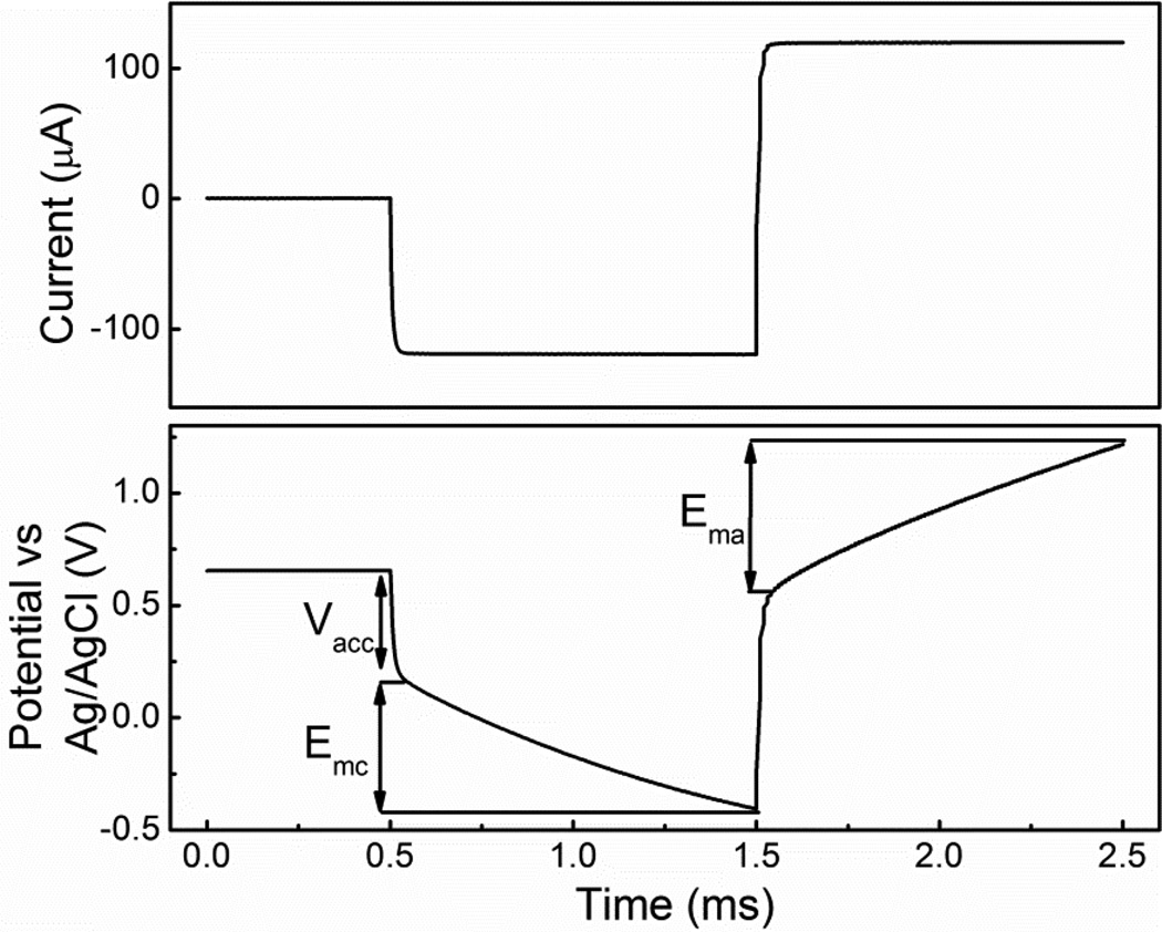
The CIC is used to measure the ability of SIROF to inject charge for stimulation applications in phosphate buffered solution (PBS, 10 mM phosphate buffer, 2.7 mM KCl and 140 mM NaCl). CIC is the total amount of charge per unit area that can be injected into the electrolyte without damaging the SIROF. The CIC measurements were performed within the voltage compliance limits of −0.6 to 0.8 V on top of the access voltage in order to avoid the dissolution of SIROF [41]. The CIC was measured by chronopotentiometry with biphasic cathodal-first pulses generated by a Gamry Reference 600 (Gamry Instruments). Fig 3 shows the measured potential of the 100 µA cathodal current pulse with a length of 1 ms following by a symmetric anodal current pulse. The access voltage (Vacc) is the resistive potential drop across the SIROF and electrolyte. The maximum cathodic and anodic electrochemical potentials (Emc and Ema) of the SIROF were calculated by subtracting Vacc from the maximum negative and positive voltage transient, respectively. The detail of this polarization method are reported by Cogan et al. [42].
Figure 3.
Voltage transient of fully deinsulated SIROF in response to the cathodal first, charge balanced biphasic current pulse in PBS. The iridium oxide working electrode, Ag/AgCl reference electrode and platinum counter electrode were immersed in PBS. The current pulse amplitude was 100 µA with length of 1 ms. The figure illustrates the maximum cathodic potential (Emc = −0.6V) and maximum anodic potential (Ema = 0.7V) during the pulse. The charge injection capacity was obtained by integrating current with time.
The SIROF CSC (mC/cm2) was measured by cyclic voltammetry in PBS solution, from −0.6 to 0.8 V with a scan rate of 50 mV/S. Also, EIS was performed to determine the impedance of SRIOF after each step of the deinsulation process, using a 10-mV sinusoidal signal from 1 Hz to 1 MHz. All the CIC, CSC and EIS measurements were conducted in PBS with a three-electrode arrangement, by using a Ag/AgCl electrode as reference electrode, a thick Pt wire as counter electrode, and iridium oxide as working electrode. Impedances of fully deinsulated electrodes of Utah electrode array (UEA) were measured by a customized automated impedance tester [43] with 10-mV RMS sine wave at 1 kHz.
4 Results and Discussion
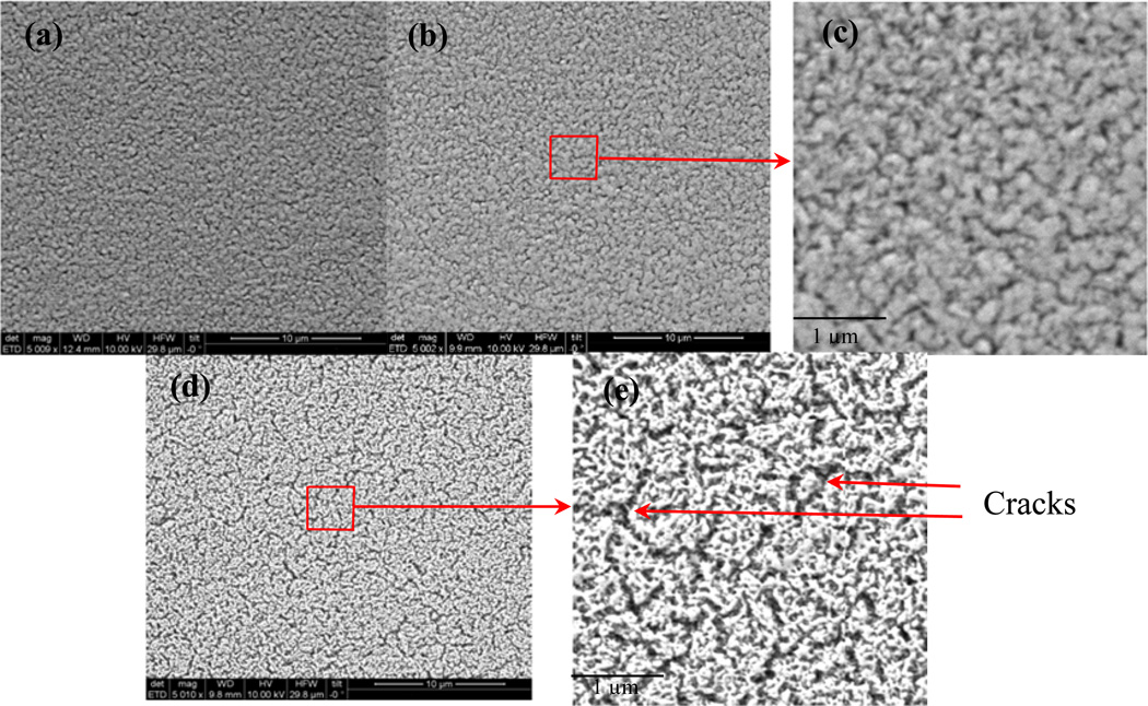
Test structures and UEA devices were fabricated to investigate the deinsulation of the process, following the procedures outlined above, and in previous reports [22, 29, 37]. The first step in the deinsulation process is to ablate the Parylene layer, using an excimer laser micromachining system. The surface morphology of the etched surface was analyzed using SEM to determine the efficacy of the Parylene remove compared to Parylene-only insulated control samples, and to characterize any damage to the alumina film or underlying layers. Fig 4 shows a set of SEM micrographs from laser ablated SIROF spots. The alumina layer was still on top of SIROF. The alumina and Parylene (A+P) coated SIROF after laser ablation (Fig 4 (b)) was similar to the as-deposited SIROF (Fig 4 (a)). However, micro cracks were clearly observed on Parylene coated SIROF after laser ablation (Fig 4 (d)), especially in detailed view (Fig 4 (e)). The micro cracks are most likely induced by the high temperature achieved during the laser ablation process. Those micro-cracks were not present in the sample using the A+P bilayer encapsulation after laser ablation (Fig 4 (c)), which suggests that alumina acted as a shield layer preventing the underlying SIROF damage thorough laser irradiation.
Figure 4.
SEM micrographs of (a) as-deposited SIROF, (b) alumina and Parylene C bilayer coated SIROF after laser ablation and (d) Parylene C coated SIROF after laser ablation. (c) and (e) are the detailed views of (b) and (d), respectively. Micro cracks were clearly observed for Parylene coated SIROF after laser ablation.
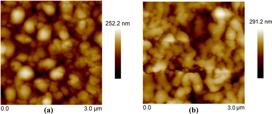
Atomic force microscopy (AFM) was also used to characterize the surface roughness and characteristic feature size of SIROF after laser ablation (Fig 5). The RMS surface roughness for as-deposited SIROF, and laser-ablated samples using both the A+P and Parylene-only encapsulation process were measured to be 39 nm, 38 nm, and 41 nm, respectively. The surface roughness after ablation was similar to as-deposited SIROF (39 nm). However, compared with the bilayer coated SIROF (Fig 5 (a)), Parylene-only coated samples (Fig 5 (b)) had slightly larger and more rounded “grain” features, consistent with a melted appearance. The characteristic features sizes for both encapsulation schemes were bigger than that of as-deposited SIROF. The heat from laser ablation and lack of shielding alumina layer led to the melting of SIROF and formation of bigger grain size for Parylene coated SIROF.
Figure 5.
AFM micrographs of (a) alumina and Parylene C coated SIROF after laser ablation, and (b) Parylene C coated SIROF after laser ablation. The A+P coated SIROF had smaller grain size and less melt compared with Parylene coated SIROF.
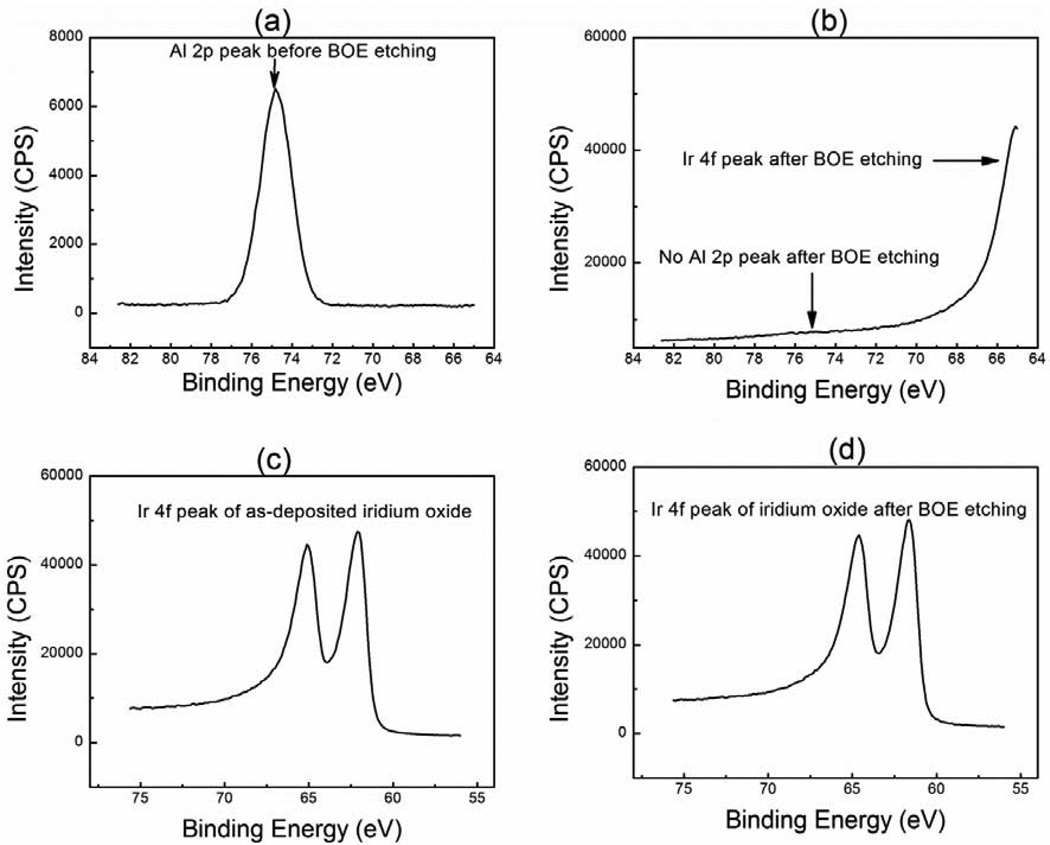
Following the laser ablation, O2 RIE process was utilized to remove the carbon residue, and BOE was used to remove alumina to expose the underlying SIROF. The O2 RIE process was characterized by CIC, CSC and EIS, as discussed in later section. XPS was utilized to confirm the BOE etching of alumina. XPS spectra were collected using a Kratos Axis-Ultra-DLD instrument with monochromatic Al Kα radiation operated at 180 W and 15 kV. The XPS was used in small-spot analysis mode to facilitate measurements during depth profiling, and utilized a spot size was 110 × 110 µm2. Table 1 presents the surface composition (at %) of the alumina coated SIROF as a function BOE etching time at room temperature. Fig 6 presents the XPS spectra of alumina coated SIROF before and after BOE etching. For the alumina coated SIROF, presence of Al 2p peak and absence of Ir 4f peaks (Fig 6 (a)) suggest a pin-hole free and conformal alumina coating. Both alumina and iridium were detected after 5 minutes of BOE etching (Table 1). No Al 2p peak was observed after 8 minutes of BOE etching and Ir 4f peaks were detected due to the exposure of SIROF (Fig 6 (b)), suggesting that alumina was completely removed. The etch rate of alumina was roughly 8±1 nm/minute. Fig 6 (c) and (d) compared the Ir 4f peaks for SIROF before (as-deposited) and after BOE etching. The similarity of those two peaks implied that BOE etching did not chemically affect the SIROF. This is consistent with SEM observations, and also consistent with the results from electrochemical characterizations presented below.
Table 1.
Surface composition (at %) measured by XPS as a function of BOE etching of 52 nm alumina coated SIROF. No Al was detected after 8 minutes of BOE etching.
| BOE Etch time (minutes) |
O 1s | C 1s | Al 2p | Ir 4f |
|---|---|---|---|---|
| 0 | 54.41 | 1.06 | 44.53 | 0 |
| 5 | 57.40 | 0 | 30 | 14.70 |
| 8 | 44.98 | 0 | 0 | 55.02 |
Figure 6.
XPS spectra of (a) Al 2p peak for alumina coated SIROF, (b) Al 2p peak for alumina coated SIROF after 8 min of BOE etching, (c) Ir 4f peak for as-deposited SIROF, and (d) Ir 4f peak for alumina coated SIROF after 8 min of BOE etching. Alumina was completely etched away and iridium oxide was exposed after 8 minutes of BOE etching. Also, as deposited SIROF has a similar Ir 4f peak character compared with SIROF after 8 minutes of BOE etching, suggesting that the three-step deinsulation process didn’t chemically affect the SIROF.
The CIC density (mC/cm2), CSC density (mC/cm2), and electrochemical impedance (Z (Ω)) of SIROF were measured after each step of deinsulation process: 1) laser ablation, 2) oxygen plasma etching, and 3) BOE etching, and compared to measurements from Parylene-only control samples.
Higher charge injection capacity (CIC) is needed to allow smaller electrodes to evoke a response and induce minimal tissue damage by injecting higher stimulation current while operating within safe voltage limits. Electrode materials with higher CIC can improve selectivity without compromising sensitivity. The CIC of A+P coated SIROF was low after laser ablation and oxygen plasma process steps, and then increased significantly from 100 nC to 325 nC after BOE etching for area of 2 × 10⁻⁴ cm2 (1.6 mC/cm2), as presented in Table 2. The low CIC density after laser ablation (0.5 mC/cm2) resulted from the existence of carbon residual and alumina coating on the SIROF surface. A slight increase in CIC after oxygen plasma etching resulted from the removal of carbon and Parylene residues, and is consistent with previously reported results [44]. The CIC density increased significantly after BOE etching (from 0.5 to 1.6 mC/cm2) due to the complete removal of alumina. For Parylene C coated SIROF control samples with the same area, the CIC density was 0.4 mC/cm2 after laser ablation. The CIC density increased dramatically to 1.1 mC/cm2 after oxygen plasma etching because of the successful removal of carbon residual on the surface. The BOE etching did not significantly affect CIC density (from 1.1 to 1.2 mC/cm2) of Parylene-only coated SIROF samples. The higher CIC density of A+P coated SIROF is attributed to protection of the SIROF by alumina during the laser ablation process. Micro-cracks, chemical reduction, and damage to SIROF films have been observed during laser deinsulation processes. We believe the alumina film is acting as a capping layer to prevent reduction of the IrOx film, and is also absorbing some portion of the laser flux, thereby protection the underlying film.
Table 2.
CIC (in nC) of SIROF with A+P and P coating after sequential etching processes of laser ablation, oxygen plasma and BOE. The CIC for A+P coated SIROF was higher than that of P coated SIROF. Also, CIC for A+P coated SIROF was increased significantly after BOE etching. The number of samples measured in each condition was 3 (N=3). Exposed areas were varied by changing the mask sizes during laser ablation.
| Area (cm2) | CIC unit |
A+P, laser |
P, laser |
A+P, oxygen plasma |
P, oxygen plasma |
A+P, BOE |
P, BOE |
|---|---|---|---|---|---|---|---|
| 2 × 10⁻⁵ | nC | 8 | 8 | 10 | 23 | 27 | 23 |
| 8 × 10⁻⁵ | nC | 8 | 25 | 8 | 100 | 120 | 110 |
| 2 × 10⁻⁴ | nC | 75 | 220 | 100 | 225 | 325 | 240 |
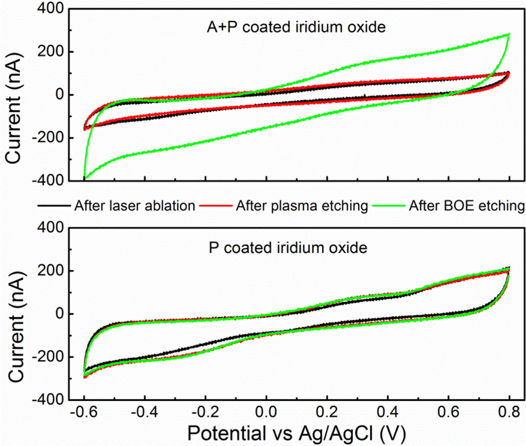
Charge storage capacity (CSC) is a measure of charge available at near equilibrium condition. The CSC of SIROF using A+P and Parylene-only encapsulation were also measured after each step in the etching process, as presented in Fig 7. The CSC was 4.2 mC for fully deinsulated A+P coated SIROF and 3.4 mC for post-etched Parylene-only coated SIROF for an area of 2 × 10⁻⁴ cm2. A+P coated SIROF had significantly lower CSC before BOE etching due to the presence of alumina on the surface of SIROF. For Parylene-only coated SIROF, CSC increased slightly after using oxygen plasma to remove the carbon residual and was identical before and after BOE etching. This indicated that BOE did not impact the electrochemical properties of SIROF.
Figure 7.
The voltammograms of iridium oxide with A+P (alumina and Parylene) and P (Parylene) coating after sequential etching processes of laser ablation (black), oxygen plasma (red) and BOE (green). The scan rate was 50 mV/s.
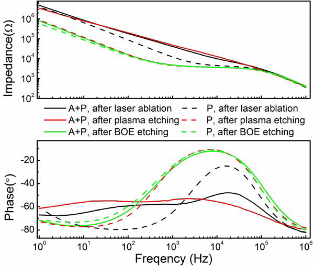
The impedance of SIROF was also characterized using electrochemical impedance spectroscopy (EIS) using a 10-mV sine wave and data from all steps of the deinsulation process from both encapsulation methods are presented in Fig 8. Impedance at 1 kHz, a characteristic frequency for action potentials, is reported in Table 3 at the three different stages of the etching process. For SIROF with Parylene coating and A+P coating, the impedance at 1 kHz after laser ablation of Parylene was 12 kΩ and 48 kΩ, respectively, for an area of 8 × 10⁻⁵ cm2. The relatively high impedance was due to the existence of carbon residual (for both Parylene coating and A+P coating) and alumina (for A+P coating only) on the surface. After oxygen plasma etching, the impedance of Parylene-only encapsulation decreased to 4.5 kΩ. The impedance for A+P encapsulation only decreased slightly to 41 kΩ, but it was much higher than Parylene coated SIROF, because of the presence of the alumina layer. After BOE etching, the impedance and its phase for SIROF with two different coatings were almost identical at ~ 4.7 kΩ with phase of −25°, which suggested the effective removal of alumina for A+P coated SIROF. Also, Parylene coated SIROF had almost the same impedance and phase before and after BOE etching, implying BOE did not have an effect on the electrochemical characteristics of the SIROF. This is consistent with the findings from XPS analysis. The fully deinsulated Parylene coated and A+P coated SIROF had almost identical impedance and phase.
Figure 8.
Bode plots of electrochemical impedance for SIROF with an area of 8 × 10⁻⁵ cm2. Impedance for Parylene coated SIROF dropped significantly after oxygen plasma and stayed almost the same after BOE etching. Impedance for A+P coated SIROF decreased slightly after oxygen plasma and reached the same level with Parylene coated SIROF after BOE etching.
Table 3.
Impedance at 1 kHz (kΩ) of iridium oxide with A+P (alumina and Parylene) and P (Parylene) coating after sequential etching processes of laser, oxygen plasma and BOE. SIROF with Parylene coating and A+P coating had very similar impedance after BOE etching.
| Area (cm2) | Impedance | A+P, laser |
P, laser |
A+P, oxygen plasma |
P, oxygen plasma |
A+P, BOE |
P, BOE |
|---|---|---|---|---|---|---|---|
| 2 × 10⁻⁵ | kΩ | 104 | 43 | 34 | 15 | 13 | 14.5 |
| 8 × 10⁻⁵ | kΩ | 48 | 12 | 41 | 4.5 | 4.8 | 4.6 |
| 2 × 10⁻⁴ | kΩ | 7.3 | 2.9 | 4.9 | 2.7 | 2.5 | 2.5 |
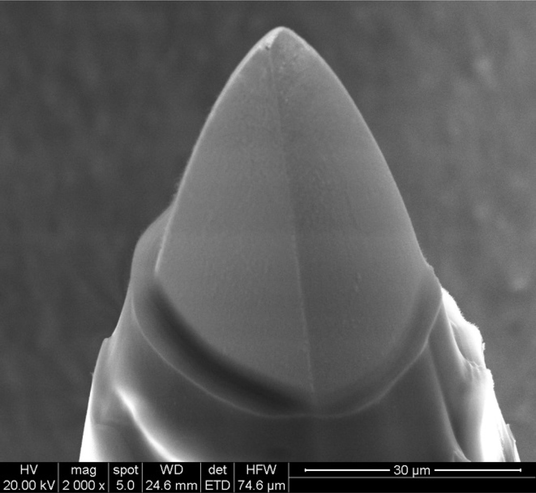
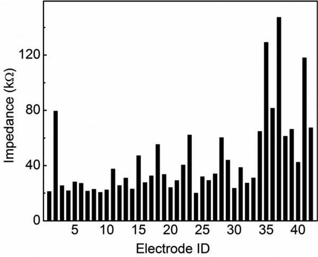
The tip of Utah electrode array after laser ablation, oxygen plasma and BOE etching is shown in Fig 9. The tip exposure was about 35 µm. The electrode impedance values are presented in Fig 10. Impedance values for most of the tips are from 20 to 50 kΩ, which are good for neural interface applications, and consistent with previously reported data for this tip deinsulation length [5]. The impedance values are relatively stable, with median of 32 kΩ and standard deviation of 30 kΩ, compared with Hsu et al. reported with standard deviation up to 50 to 100 kΩ [5]. The stability of impedance implies the relative consistency of the tip exposure because impedance is very sensitive to tip exposure variation. The ability to control tip exposure is one of the significant advantages for laser-based deinsulation technique. The variation of tip impedance could result from electrode non-uniformity during the array fabrication.
Figure 9.
Alumina and Parylene C coated tip of Utah electrode array after laser ablation, oxygen plasma etching and BOE etching.
Figure 10.
Impedance of A+P coated electrodes from Utah electrode array after laser ablation, oxygen plasma and BOE etching. Typical tip exposure is around 30 µm. The impedances are mostly in the range of 20 to 50 kΩ.
5 Conclusion
A self-aligned three-step etching process for alumina and Parylene C coated Utah electrode array that utilizes laser ablation, oxygen plasma and BOE etching, was successfully demonstrated. The alumina was found to prevent the formation of micro-cracks in the underlying iridium oxide during laser ablation. The removal of Parylene C and alumina was confirmed by XPS analysis, which showed the absence of the Al 2p peak and presence of the Ir 4f peaks. The etch rate was found to be 8 nm/minute for BOE etching of alumina. Chronopotentiometry, cyclic voltammetry, and EIS were used to characterize the electrochemical properties of deinsulated SIROF. Compared with Parylene-only encapsulation, the SIROF with A+P encapsulation had higher CIC density (240 vs 320 nC), higher CSC (3.4 vs 4.2 mC) and similar impedance (2.5 vs 2.5 kΩ) for an area of 2 × 10⁻⁴ cm2. Three-step deinsulated electrodes of Utah electrode array with bilayer coating had median impedance of 32 kΩ with standard deviation of 30 kΩ. This is more uniform compared with electrode impedance (standard deviation up to 100 kΩ) obtained through oxygen plasma etching using aluminum foil as mask. Due to its selfaligning nature, this three-step deinsulation method can be applied to many other biomedical implantable devices that require selective etching of the encapsulation, to reduce the complexity of the micromachining process and achieve more precise control of the process.
Acknowledgements
The authors would like to thank staff at the Micron microscopy core and Nanofab at the University of Utah for their support fabrication, imaging and XPS. Funding of this research is provided by DARPA contract No: N66001-06-C-4056 and NIH contract No: 1R01NS064318-01A1. Sandeep Negi and Florian Solzbacher have financial interest in Blackrock microsystems, which develops and produces implantable neural interfaces. The views expressed are those of the authors and do not reflect the official policy or position of the Department of Defense or the U.S. Government. Approved for public release; distribution unlimited.
References
- 1.Deuschl G, Schade-Brittinger C, Krack P, Volkmann J, Schäfer H, Bötzel K, et al. A randomized trial of deep-brain stimulation for Parkinson's disease. New England Journal of Medicine. 2006;355:896–908. doi: 10.1056/NEJMoa060281. [DOI] [PubMed] [Google Scholar]
- 2.Kim S, Bhandari R, Klein M, Negi S, Rieth L, Tathireddy P, Toepper M, Oppermann H, Solzbacher F. Integrated wireless neural interface based on the Utah electrode array. Biomedical microdevices. 2009;11:453–466. doi: 10.1007/s10544-008-9251-y. [DOI] [PubMed] [Google Scholar]
- 3.Peterson NR, Pisoni DB, Miyamoto RT. Cochlear implants and spoken language processing abilities: Review and assessment of the literature. Restorative neurology and neuroscience. 2010;28:237–250. doi: 10.3233/RNN-2010-0535. [DOI] [PMC free article] [PubMed] [Google Scholar]
- 4.Eckhorn R, Wilms M, Schanze T, Eger M, Hesse L, Eysel UT, et al. Visual resolution with retinal implants estimated from recordings in cat visual cortex. Vision Research. 2006;46:2675–2690. doi: 10.1016/j.visres.2006.01.034. [DOI] [PubMed] [Google Scholar]
- 5.Hsu JM, Rieth L, Normann RA, Tathireddy P, Solzbacher F. Encapsulation of an integrated neural interface device with Parylene C. Biomedical Engineering, IEEE Transactions on. 2009;56:23–29. doi: 10.1109/TBME.2008.2002155. [DOI] [PubMed] [Google Scholar]
- 6.Seymour JP, Elkasabi YM, Chen HY, Lahann J, Kipke DR. The insulation performance of reactive parylene films in implantable electronic devices. Biomaterials. 2009;30:6158–6167. doi: 10.1016/j.biomaterials.2009.07.061. [DOI] [PMC free article] [PubMed] [Google Scholar]
- 7.Hassler C, von Metzen RP, Ruther P, Stieglitz T. Characterization of parylene C as an encapsulation material for implanted neural prostheses. Journal of Biomedical Materials Research Part B: Applied Biomaterials. 2010;93:266–274. doi: 10.1002/jbm.b.31584. [DOI] [PubMed] [Google Scholar]
- 8.Xie XZ, Rieth L, Tathireddy P, Solzbacher F. Long-term in-vivo Investigation of Parylene-C as Encapsulation Material for Neural Interfaces. Procedia Engineering. 2011;25:483–486. [Google Scholar]
- 9.Hassler C, von Metzen RP, Ruther P, Stieglitz T. Characterization of parylene C as an encapsulation material for implanted neural prostheses. Journal of Biomedical Materials Research Part B: Applied Biomaterials. 2010;93B:266–274. doi: 10.1002/jbm.b.31584. [DOI] [PubMed] [Google Scholar]
- 10.Fortin JB, Lu TM. Chemical vapor deposition polymerization: the growth and properties of parylene thin films. Norwell, Massachusetts: Springer; 2004. [Google Scholar]
- 11.Licari JJ. Coating Materials for Electronic Applications - Polymers, Processes, Reliability, Testing. Norwich, New York: William Andrew Publishing/Noyes; 2003. [Google Scholar]
- 12.Westedt U, Wittmar M, Hellwig M, Hanefeld P, Greiner A, Schaper AK, Kissel T. Paclitaxel releasing films consisting of poly(vinyl alcohol)-graft-poly(lactide-co-glycolide) and their potential as biodegradable stent coatings. Journal of Controlled Release. 2006;111:235–246. doi: 10.1016/j.jconrel.2005.12.012. [DOI] [PubMed] [Google Scholar]
- 13.Szwarc M. Poly-para-xylelene: Its chemistry and application in coating technology. Polymer Engineering and Science. 1976;16:473–479. [Google Scholar]
- 14.Li W, Rodger DC, Menon P, Tai YC. Corrosion Behavior of Parylene-Metal-Parylene Thin Films in Saline. ECS Transactions. 2008;11:1–6. [Google Scholar]
- 15.Kane SR, Cogan SF, Ehrlich J, Plante TD, McCreery DB. Electrical performance of penetrating microelectrodes chronically implanted in cat cortex. 2011:5416–5419. doi: 10.1109/IEMBS.2011.6091339. [DOI] [PMC free article] [PubMed] [Google Scholar]
- 16.Xie X, Rieth L, Merugu S, Tathireddy P, Solzbacher F. Plasma-assisted atomic layer deposition of Al 2O 3 and parylene C bi-layer encapsulation for chronic implantable electronics. Applied physics letters. 2012;101 doi: 10.1063/1.4748322. [DOI] [PMC free article] [PubMed] [Google Scholar]
- 17.Minnikanti S, Diao G, Pancrazio JJ, Xie X, Rieth L, Solzbacher F, Peixoto N. Lifetime assessment of atomic-layer-deposited Al2O3–Parylene C bilayer coating for neural interfaces using accelerated age testing and electrochemical characterization. Acta Biomaterialia. 2014;10:960–967. doi: 10.1016/j.actbio.2013.10.031. [DOI] [PubMed] [Google Scholar]
- 18.Xie X, Rieth L, Tathireddy P, Solzbacher F. Atomic layer deposited Al2O3 and parylene C dual-layer encapsulation for biomedical implantable devices; Solid-State Sensors, Actuators and Microsystems (TRANSDUCERS & EUROSENSORS XXVII), 2013 Transducers & Eurosensors XXVII: The 17th International Conference on, 2013; pp. 1044–1047. [Google Scholar]
- 19.Normann RA. Technology Insight: Future neuroprosthetic therapies for disorders of the nervous system. Nature Clinical Practice Neurology. 2007;3:444–452. doi: 10.1038/ncpneuro0556. [DOI] [PubMed] [Google Scholar]
- 20.Loeb GE, Bak MJ, Salcman M, Schmidt EM. Parylene as a chronically stable, reproducible microelectrode insulator. IEEE Transactions on Biomedical Engineering. 1977;24:121–128. doi: 10.1109/TBME.1977.326115. [DOI] [PubMed] [Google Scholar]
- 21.Meng E, Li PY, Tai YC. Plasma removal of Parylene C. Journal of Micromechanics and Microengineering. 2008;18 [Google Scholar]
- 22.Campbell PK, Jones KE, Huber RJ, Horch KW, Normann RA. A silicon-based, three-dimensional neural interface: Manufacturing processes for an intracortical electrode array. IEEE Transactions on Biomedical Engineering. 1991;38:758–768. doi: 10.1109/10.83588. [DOI] [PubMed] [Google Scholar]
- 23.Ji J, Tay FEH, Miao J, Iliescu C. Microfabricated microneedle with porous tip for drug delivery. Journal of Micromechanics and Microengineering. 2006;16:958–964. [Google Scholar]
- 24.Bhandari R, Negi S, Rieth L, Normann RA, Solzbacher F. A novel masking method for high aspect ratio penetrating microelectrode arrays. Journal of Micromechanics and Microengineering. 2009;19 [Google Scholar]
- 25.Esashi M, Minami K, Shoji S. Optical exposure systems for three-dimensional fabrication of microprobe. 1991:39–44. [Google Scholar]
- 26.Loeb GE, Peck RA, Martyniuk J. Toward the ultimate metal microelectrode. Journal of Neuroscience Methods. 1995;63:175–183. doi: 10.1016/0165-0270(95)00107-7. [DOI] [PubMed] [Google Scholar]
- 27.Schmidt EM, Bak MJ, Christensen P. Laser exposure of Parylene-C insulated microelectrodes. Journal of Neuroscience Methods. 1995;62:89–92. doi: 10.1016/0165-0270(95)00060-7. [DOI] [PubMed] [Google Scholar]
- 28.Choi Y, Choi SO, Shafer RH, Allen MG. Highly inclined electrodeposited metal lines using an excimer laser patterning technique. 2005:1469–1472. [Google Scholar]
- 29.Yoo J-M, Sharma A, Tathireddy P, Rieth LW, Solzbacher F, Song J-I. Excimer-laser deinsulation of Parylene-C coated Utah electrode array tips. Sensors and Actuators B: Chemical. 2012;166–167:777–786. [Google Scholar]
- 30.Koo S-M, Kim D-P, Kim K-T, Kim C-I. The etching properties of Al2O3 thin films in N2/Cl2/BCl3 and Ar/Cl2/BCl3 gas chemistry. Materials science & engineering. B, Solid-state materials for advanced technology. 2005;118:201–204. [Google Scholar]
- 31.Fukushima N, Katai H, Wada T, Horiike Y. High-Rate and Smooth Surface Etching of Al2O3-TiC Employing Inductively Coupled Plasma (ICP) Japanese Journal of Applied Physics-Part 1 Regular Papers and Short Notes. 1996;35:2512–2515. [Google Scholar]
- 32.Kim JW, Kim YC, Lee WJ. Reactive ion etching mechanism of plasma enhanced chemically vapor deposited aluminum oxide film in CF4/O2 plasma. Journal of Applied Physics. 1995;78:2045–2049. , // [Google Scholar]
- 33.Carcia PF, McLean RS, Reilly MH. Permeation measurements and modeling of highly defective Al2 O3 thin films grown by atomic layer deposition on polymers. Applied physics letters. 2010;97:221901 1–221901 3. [Google Scholar]
- 34.Bulusu A, Kim H, Samet D, Graham S., Jr Improving the stability of atomic layer deposited alumina films in aqueous environments with metal oxide capping layers. Journal of Physics D: Applied Physics. 2013;46:084014 1–084014 10. [Google Scholar]
- 35.Abdulagatov AI, Yan Y, Cooper JR, Zhang Y, Gibbs ZM, Cavanagh AS, Yang RG, Lee YC, George SM. Al2O3 and TiO2 atomic layer deposition on copper for water corrosion resistance. ACS Applied Materials & Interfaces. 2011 Dec;3:4593–4601. doi: 10.1021/am2009579. 2011. [DOI] [PubMed] [Google Scholar]
- 36.Yoo JM, Song JI, Tathireddy P, Solzbacher F, Rieth LW. Hybrid laser and reactive ion etching of Parylene-C for deinsulation of a Utah electrode array. Journal of Micromechanics and Microengineering. 2012;22 [Google Scholar]
- 37.Bhandari R, Negi S, Rieth L, Solzbacher F. A wafer-scale etching technique for high aspect ratio implantable MEMS structures. Sensors and Actuators, A: Physical. 2010;162:130–136. doi: 10.1016/j.sna.2010.06.011. [DOI] [PMC free article] [PubMed] [Google Scholar]
- 38.Xie X, Rieth L, Caldwell R, Diwekar M, Tathireddy P, Sharma R, Solzbacher F. Long-Term Bilayer Encapsulation Performance of Atomic Layer Deposited Al2O3 and Parylene C for Biomedical Implantable Devices. Biomedical Engineering, IEEE Transactions on. 2013;60:2943–2951. doi: 10.1109/TBME.2013.2266542. [DOI] [PubMed] [Google Scholar]
- 39.Negi S, Bhandari R, Rieth L, Solzbacher F. Effect of sputtering pressure on pulsed-DC sputtered iridium oxide films. Sensors and Actuators, B: Chemical. 2009;137:370–378. [Google Scholar]
- 40.Xie X, Rieth L, Cardwell R, Sharma R, Yoo JM, Diweka M, Tathireddy P, Solzbacher F. Bi-layer encapsulation of utah array based nerual interfaces by atomic layer deposited Al2O3 and parylene C; Solid-State Sensors, Actuators and Microsystems (TRANSDUCERS & EUROSENSORS XXVII), 2013 Transducers & Eurosensors XXVII: The 17th International Conference on 2013; pp. 1267–1270. [Google Scholar]
- 41.Negi S, Bhandari R, Rieth L, Van Wagenen R, Solzbacher F. Neural electrode degradation from continuous electrical stimulation: Comparison of sputtered and activated iridium oxide. Journal of Neuroscience Methods. 2010;186:8–17. doi: 10.1016/j.jneumeth.2009.10.016. [DOI] [PMC free article] [PubMed] [Google Scholar]
- 42.Cogan SF, Troyk PR, Ehrlich J, Plante TD, Detlefsen DE. Potential-biased, asymmetric waveforms for charge-injection with activated iridium oxide (AIROF) neural stimulation electrodes. IEEE Transactions on Biomedical Engineering. 2006;53:327–332. doi: 10.1109/TBME.2005.862572. [DOI] [PubMed] [Google Scholar]
- 43.Gunalan K, Warren DJ, Perry JD, Normann RA, Clark GA. An automated system for measuring tip impedance and among-electrode shunting in high-electrode count microelectrode arrays. Journal of Neuroscience Methods. 2009;178:263–269. doi: 10.1016/j.jneumeth.2008.12.020. [DOI] [PubMed] [Google Scholar]
- 44.Yoo J-M, Negi S, Tathireddy P, Solzbacher F, Song J-I, Rieth LW. Excimer laser deinsulation of Parylene-C on iridium for use in an activated iridium oxide film-coated Utah electrode array. Journal of Neuroscience Methods. 2013 Apr 30;215:78–87. doi: 10.1016/j.jneumeth.2013.02.010. [DOI] [PMC free article] [PubMed] [Google Scholar]


