Abstract
We report for the first time a successful fabrication and operation of an InAs/GaAs quantum dot based intermediate band solar cell concentrator photovoltaic (QD-IBSC-CPV) module to the IEC62108 standard with recorded power conversion efficiency of 15.3%. Combining the measured experimental results at Underwriters Laboratory (UL®) licensed testing laboratory with theoretical simulations, we confirmed that the operational characteristics of the QD-IBSC-CPV module are a consequence of the carrier dynamics via the intermediate-band at room temperature.
The intermediate-band solar cell (IBSC) is one of the most promising candidates for the next generation of photovoltaic devices, with a detailed balance efficiency of 63.2% under idealised conditions and maximum concentration1. IBSCs require light concentration not only to reduce the device cost but also to ensure optimal operation when carrier photogeneration is outperforming the recombination processes via the intermediate-band (IB). Although the intermediate-band term is used exstensively in the literature for this concept of SC device, we would like to point out that those are actually a collection of intermediate-states of quantum dots in a particular surface or vertical arrangement, and not necessarily perfectly periodic or infinite. To date, great effort has been devoted to the fabrication of IBSC devices based on inorganic quantum dots and the study of their principle of operation2,3,4,5,6,7,8,9,10,11, with limited or no evidence of IB operation. Despite significant advances, evaluation of carrier dynamics via IB for an IBSC in a concentrating photovoltaic (CPV) module configuration presents both fundamental and technical obstacles, limiting its application and possible future commercialisation.
We report here the first successful fabrication of an InAs/GaAs quantum dot based IBSC concentrator photovoltaic (QD-IBSC-CPV) that works in the IBSC regime, with recorded power conversion efficiency of 15.3%. Following experimental results and theoretical simulations, we confirm that the operation characteristics of the QD-IBSC-CPV module are a consequence of carrier dynamics via states in the intermediate-band at room temperature, and not thermal escape.
The concentrating photovoltaic (CPV) module contains solar receivers and concentrating optical systems. Fig. 1 shows a picture of the fabricated CPV module, which contains two separate parts with four series-connected GaAs control sub-modules on one side and four InAs/GaAs QD-IBSC-CPV sub-modules on the other. The InAs/GaAs QD-IBSC-CPV and GaAs control cell were fabricated by adopting a p – i – n cell structure on an n-type GaAs (001) substrate using the molecular beam epitaxial method. Details regarding the structure of the solar cell designs are presented in supplementary information S1.
Figure 1.
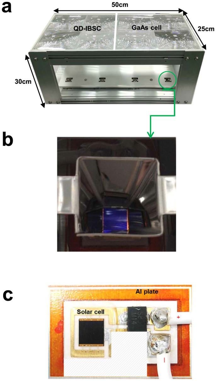
(a) Picture of the fabricated CPV module. (b) A close-up of the secondary optics. The solar cell was covered by a transparent silicon-gel for protection. (c) The submount of the IBSC on aluminium heat sink plate, where a developed plane soldering technique has been employed to maximise the heat dissipation. A blocking diode was also integrated into the circuit to prevent reverse biasing.
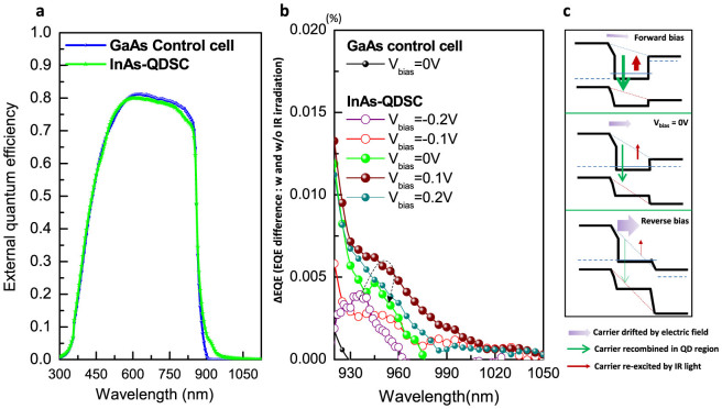
First, we investigated the IB carrier dynamics of the QD-IBSC without light concentration, in order to verify the suitability of samples before integration into the CPV module. To assess the IB dynamics we employed the infrared biased external quantum efficiency (IR-EQE) method at room temperature (RT)2,9. Since the EQE is the ratio of collected carriers to incident photons at given wavelength hitting the SC, it is a measure of both the absorption and carrier collection. It involves a two-step photo-absorption process at the IB of the QD ensemble due to the IR light illumination. It detects experimentally the difference in the RT-EQE signal between samples measured without IR bias light and those sequentially illuminated by IR light during the test. Due to the very weak RT-IR-EQE signal, the measurement is extremely sensitive to noise. Details regarding the background signal, signal/noise ratio, and the experimental uncertainties are given in supplementary material S2. Fig. 2(a) shows the normal RT-EQE (without IR) for both the GaAs control cell and InAs/GaAs QD-IBSC. Compared to the GaAs control cell, the EQE signal of the InAs/GaAs QD-IBSC beyond 900 nm (the GaAs absorption edge) is clearly visible. These signals were attributed to carriers that were excited from the valence band (VB) to IB states of the QDs and were then thermally excited and collected by the electrode. The RT-IR-EQE results are given in Fig. 2(b). We focus our attention on the region between 920 nm and 1050 nm, where the reliability of the signal was confirmed. Compared to the negligible signal of the GaAs control cell, the InAs/GaAs QD-IBSC exhibits a visible spectral response owing to the IR light illumination. An enhanced EQE signal was detected that can only be attributed to the optical transitions from IB states of the QDs to the higher band above the GaAs conduction band edge9. In order to verify further the origin of the enhanced IR-EQE signal in the InAs/GaAs QD-IBSC, a bias voltage was applied to the sample and varied from −0.2 V to +0.2 V. The effect of the bias voltage on the RT-IR-EQE signal is schematically presented in Fig. 2(c). When the sample is under forward bias, the number of carriers drifting across the QD due to the pn-junction electric field is reduced. This increases the number of carrier captured within the QD, therefore enhancing the IB-CB absorption under IR illumination. On the other hand, when the sample is under reverse bias, the carrier drift velocity is greatly increased, thus reducing the probability of carriers being captured, and consequently excited by IR photons in the QD region, Fig. 2(c). Experimentally, we observed a similar tendency, wherein the RT-IR-EQE signal increases with increase of the forward bias voltage. Excessive increase of the forward bias voltage tends to reduce the IR-EQE signal as carrier capture becomes dominant and strongly suppresses carrier excitation out of the barrier by IR photons.
Figure 2.
(a) Experimental results of EQE measured at room temperature for both QD-IBSC-CPV and GaAs control cell. (b) EQE difference of solar cell with and without infrared (IR) bias light irradiation as well as the voltage bias dependence. (c) Schematic illustration of bias voltage effect on the intermediate-state carrier dynamics.
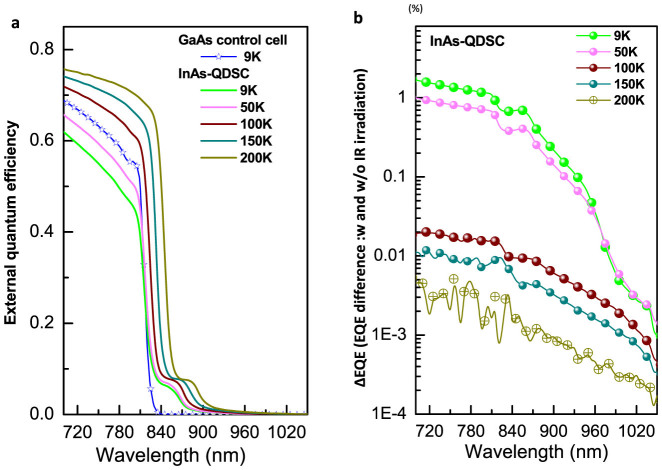
It is generally accepted that at room temperature, the majority of carriers are excited out of the QD's potential from the IB by thermal excitation, therefore dramatically reducing the number of carriers participating in two-step photo-absorption. This is the main reason for the weak RT-IR-EQE signal shown in Fig. 2(b). In order to confirm the more pronounced intermediate band features in the InAs/GaAs QD-IBSC samples, we conducted IR-EQE measurements at low temperature (LT-IR-EQE). The LT-IR-EQE experiment was performed using our bespoke equipment, with a basic set-up similar to those reported elsewhere2. The wavelength of the filtered IR bias light was longer than 1500 nm and the IR light was chopped at a frequency of 233 Hz. Fig. 3(a) shows a series of representative low temperature EQE results. It is clearly seen here that decreasing the temperature tends to shift the absorption edge of the InAs/GaAs QD-IBSC to a shorter wavelength. We also found that decreasing temperature suppresses carrier collection for both the InAs/GaAs QD-IBSC and GaAs control cell in the range between 700 nm–820 nm. Fig. 3(b) shows LT-IR-EQE results and a dramatically enhanced IR-EQE, of for more than 1%, found for the InAs/GaAs-QDSC at 9K. Since thermal excitation at this temperature can be completely ruled out, the observed increase of 1% in the IR-EQE is solely attributed to the radiative carrier generation. This generation can only originate from two-step photo-absorption involving the IB states, under IR illumination, indicating that the IB is functioning well in our samples.
Figure 3.
(a) Low temperature experimental results of EQE for both QD-IBSC and GaAs control cell. (b) Low temperature EQE difference of solar cell with and without infrared (IR) bias light irradiation.
Having confirmed the carrier dynamics via IB-states for the selected InAs/GaAs QD-IBSC samples, we proceeded with the integration of those cells into the CPV module and investigated the IB-state carrier dynamics under light concentration.
The QD-IBSC-CPV module characterisations were performed at room temperature using HELIOS 3198, a standard CPV measurement system with a flash lamp as a light source. Fig. 4(a) shows the current-voltage curves of the QD-IBSC-CPV and GaAs control modules measured under light concentration of 116 suns. We obtained a conversion efficiency of η = 19.2% for the GaAs control module and η = 15.3% for the InAs/GaAs QD-IBSC-CPV module. In Fig. 4(b) the measured efficiency η(X) is given as a function of the concentration ratio, X. For the GaAs control CPV module, we found that its efficiency reaches a peak plateau in the range X≈140–160 suns and quickly falls off for values of X beyond this. For the QD-IBSC-CPV module the peak plateau is located at around X≈110–130 suns. Theoretically, η(X) increases logarithmically with respect to X, as long as the linearity of the short circuit current, Isc, as a function of X holds12. However, since the increase in concentration ratio causes an increase in current, this effect offsets the voltage gained from the light concentration by a potential drop due to the existence of series resistance, Rs, at the electrodes. We have simulated η(X) by using the parametric method13, in which the “loss factor” is given as  , where Jm and Vm are the current and voltage at the maximum operation point. The loss factor represents the fraction of the output power delivered by the solar cell that is lost due to the finite value of Rs. Fitted results shown in Fig. 4(a) were obtained with Rs = 0.05 Ωcm2 for both modules. The diode ideality factor was set as 1.0 for the GaAs control module and 1.5 for the QD-IBSC-CPV based module, in order to take into account the existence of an additional recombination path via the IB.
Figure 4.
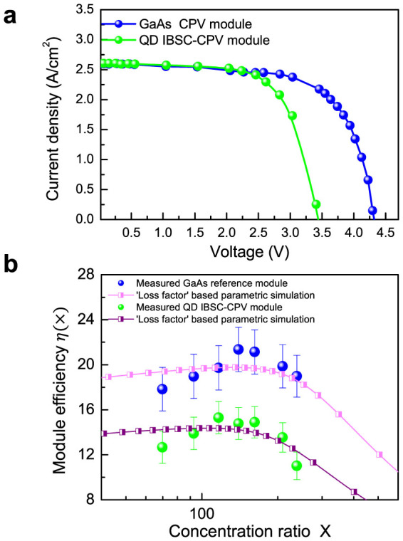
(a) Current-voltage curve of the IBSC-CPV module and GaAs control module. (b) Conversion efficiency η(X) under different concentration ratio, X. Fitted results, based on “loss factor” parametric method, are also presented.
In order to identify the role of the IB in radiative processes, we proceed our analysis with a detailed investigation of the dependence of Isc and Voc on the concentration ratio, X, in CPV modules. The data shown in Fig. 5 are the normalised Isc(X)/Isc(X = 1sun) and Voc(X)/Voc(X = 1sun) using results from all four sub-modules. In Fig. 5(a), we clearly noticed a different rate of increase in Isc(X)/Isc(X = 1sun) between the GaAs control and the QD-IBSC-CPV module. First, we took an average of Isc of all four sub-modules and then performed a linear regression analysis, based on a linear least square fitting algorithm. We found that the rate at which Isc(X) increases with X, or the slope, dIsc(X)/dX, of the GaAs control module is 0.0061, while the slope for the QD-IBSC-CPV module is 0.0070. As shown in the theoretical analysis below, an increase of dIsc(X)/dX in the QD-IBSC-CPV module, when compared to the GaAs control cell, is one of the decisive signatures of the proper electron dynamics in an IBSC under light concentration.
Figure 5.
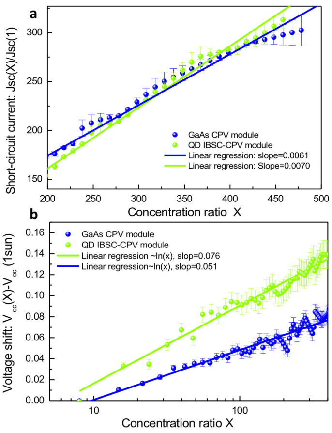
(a) Linear regression fitting of Isc(X) with least square error bars. (b) Linear regression fitting of Voc(X) with least square error bar. Note here that the Voc(X) was shifted by the amount of Voc(1sun) for better comparison.
Results for the open circuit voltage, Voc(X) vs. X for all four sub-modules are shown in Fig. 5(b). We found that the Voc of the QD-IBSC-CPV module is about ~0.25 V lower than in the GaAs control module. The amount of this reduction is consistent with our previous reports14,15. Lower Voc(X) in the QD-IBSC-CPV module is mainly due to the fact that recombination via the IB is still prominent. In addition, the VB-CB energy gap in an InAs QD-IBSC is usually smaller than the VB-CB energy band gap of a GaAs cell, which causes greater thermalization of the VB states, i.e., greater dark saturation current. This is therefore also responsible for the reduction of Voc. Meanwhile, the non-radiative recombination via defects formed at the InAs/GaAs QD hetero-interface is also partly responsible for the observed reduction in Voc. Fig. 5(b) show results of the linear regression fitting, similar as for Isc. We conclude that there is a clear increase of dVoc(X)/dX for all four QD-IBSC-CPV modules, when compared to the GaAs control.
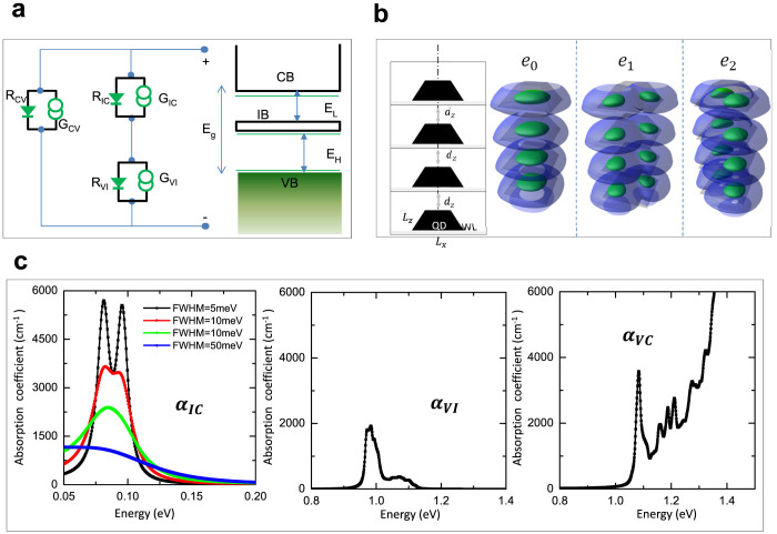
In order to gain a better understanding of the experimental results, we performed theoretical calculations to identify carrier dynamics of the QD-IBSC-CPV under light concentration. A schematic model of the IBSC is shown in Fig. 6(a). The current continuity equation for electrons and holes under steady state is given, including IB, as  , where v denotes the type of carriers (e or h) and
  ,
,  ,
,  are the electron or hole density of the CB, VB, and IB respectively. Gij and Rij (see Fig. 6(a)) are the carrier generation and recombination rates among different bands, i and j, respectively. In the steady state, which relevant for SC operation, ∂/∂t = 0. We applied the charge conservation rule,
  , where
  is the pre-filled donor concentration of the IB. In addition, in order to accurately determine the parameter set for the drift-diffusion model, the multiband k · p method for the electronic structure of the QD arrays, with periodic boundary conditions, was used16. From electronic structure model we have obtained information such as the density of states and band gap energies, as well as the respective optical absorption coefficients in the dipole approximation:
 |
where, i, f ∈ (VB, IB, CB), K is the wave vector of the QD array Brillouin zone,  is the polarisation sensitive optical dipole matrix element, Ω = Lx × Ly × Lz is the volume of the primitive cell of the QD array, where Lz = dz + h + LWL, and δ is the spectral line with line broadening Γ17. In our electronic structure simulation, we have used experimental structure parameters for the QDs: base length of b = 15 nm, height, h = 4 nm, and truncation factor t = 0.5. Vertical periodicity of the QD array is controlled by the distance between the top of the QD in nth layer and the bottom of the wetting layer in the (n + 1)th layer growth, and set to dz = 5 nm. Partly delocalised charge density of IB's states e0 and e1 in the CB and h0 and h1 in VB are given in Fig. 6(b). Assuming favourable dynamical conditions, that support the formation of quasi-Fermi level separation between CB–IB, VB–IB, and VB–(CB-IB) (where the latter denotes the separation between states in the VB and those in the CB without IB states), the absorption spectra of the QD-IBSC can be decomposed into three different absorption pathways, as shown in Fig. 6(c). It should be noted that, while αV,I and αV,C occure between interband transitions, dominated by the radiative processes and narrow line broadening of, Γ = 5 meV, αI,C occurs due to intraband transitions, which are dominated by much faster nonradiative processes, with much larger and more uncertain line broadening.
Figure 6.
(a) Drift-diffusion model adopted for IBSC. GV I, GIC, GVC, stand for photon generation while RVI, RIC, RVC stand for recombination, where the indices V, I, and C correspond to the valence band, intermediate band and conduction band respectively. Three quasi-Fermi levels (green line) are also given for each band. (b) Geometric information of QD and QD array used in multi-band kp calculation. The unit box is represented by three sides of length of Lx, Ly and Lz26. (c) Absorption coefficients between IB and CB, VB and IB, and VB and rest of CB.
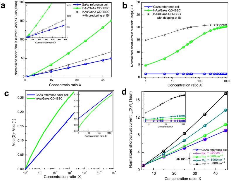
Theoretically, for a conventional solar cell under a moderate (several hundred) value of X, Isc increases linearly while Voc increases logarithmically with respect to X. However, this is not valid for the IBSC even at low concentration ratios. As shown in Fig. 7(a), when compared to the linear variation of Isc for the GaAs control cell, the Isc of the QD-IBSC-CPV shows a distinct non-linear behaviour. It is apparent that the increase of dIsc/dX for the QD-IBSC-CPV is much larger than that for the GaAs control cell. This confirms our experimental findings shown in Fig. 4(b). Therefore, we conclude that the larger rate at which Isc increases with X, observed for the QD-IBSC-CPV module, is a direct consequence of the carrier dynamics via the IB. To examine the linearity of Isc in more detail, we normalised Isc with concentration ratio X, Fig. 7(b). For the GaAs control cell, such a normalised figure is a constant indicating a linear increase of dIsc/dX. However, in contrast to the GaAs control cell, Isc(X)/X of the QD-IBSC-CPV shows a logistic-like profile, indicating a strong nonlinear dependence of Isc(X)/X on X. The difference in behaviour of the QD-IBSC-CPV from the GaAs control cell arises from the complexity of the carrier generation rates associated with the electron occupancy of the IB18. As light concentration ratio X increases, the photofilling effects come into play and the generation rate of the IB is greatly enhanced.
Figure 7.
(a) Calculated short circuit current Isc for QD-IBSC and GaAs control cell under different concentration ratio. Isc(X) ∝ X of IBSC with predoping in IB is also presented (black curve). To compare with experimental data, Isc(X) is normalised by Isc(1sun). (b) Non-linear feature of Isc(X) of IBSC. Here the Isc(X) is normalised by concentration ratio X and the horizontal axis is set on log scale. (c) Calculated open circuit voltage Voc for QD-IBSC and GaAs control cell under different concentration ratio X. Voc(X) is shifted by Voc(1sun) for better comparison with experimental data. (d) Calculated Isc(X) ∝ X for QD-IBSC under different absorption coefficients of the transition from IB to CB.
The simulation results for Voc of QD-IBSC-CPV show a similar tendency to Isc. The increased rate of Voc is much larger for the QD-IBSC-CPV than for the GaAs control cell, especially at low X (below 50–100 suns), Fig. 7(c). The inset in Fig. 7(c) shows that Voc of the IBSC is initially lower than that of the GaAs control cell, but reaches a comparable value when X exceeds 1000 suns. The increase of Voc with X is attributed to the fact that a larger voltage is required to reduce the large net carrier generation via the IB and to maintain the aforementioned IB continuity.
It is worth mentioning that there has been a general concern regarding the carrier dynamics involving Isc enhancement via the IB in the InAs/GaAs QD-IBSC at room temperature (RT), due to the thermal fluctuation7,19. Our group has reported several successful observations of two–step photon absorption via the IB at RT in samples such as Si doped InAs/GaAs QD-IBSC9,15. We have found that the suppression of non-radiative recombination loses and the pre-filling of IB due to Si doping played decisive roles in the observation of two–step carrier dynamics at RT. In the current work, InAs/GaAs QD-IBSC was prepared without doping. We attribute the observed carrier dynamics via the IB to the fact that the light concentration has played a similar role to the IB as a pre-filling of the IB in our previous samples9. It is known that pre-doping and photo-filling of the IB20 play similar roles, which have also been confirmed in our simulation, see Fig. 7(a,b). Meanwhile, it has been reported that the light concentration induced high level of injection can effectively saturate the Shockley-Read-Hall (SRH) type defects, thus suppressing the non-radiative recombination in a multi-quantum well GaAs/AlGaAs solar cell21. According to the SRH kinetic statistics, while assuming an n-type material with doping concentration, ND, the capture rate for the minority carrier (hole) can be written as: Rp ∝ N−Δp, where N− is the density of negatively charged defect levels and Δp is the injected carrier concentration. At high injection level, Δp/ND becomes very large and N− → 0, since Rp is approximately constant. Therefore the recombination centres are saturated for minority carriers22. In addition, except for the thermal fluctuation effect mentioned above, we have also studied the effect of optical absorption from the IB to the CB on the variation of Isc(X) as a function of X. The results are summarised in Fig. 7(d). It shows that for IB to CB absorption coefficients as small as 100 cm−1, the difference in dIsc(X)/dX vs. X, between the QD-IBSC-CPV module and GaAs control module becomes indistinguishable. However, when the IB to CB absorption coefficient increases to  , which is below the reported experimental value for the VB to IB absorption coefficient23, the difference in dIsc(X)/dX becomes clearly distinctive. Based on our k · p calculations, a low intraband absorption coefficient value such as 500 cm−1 can be obtained by assuming large line broadening,
  . Such a large broadening is fully justified by very fast dynamical intraband nonradiative dynamical processes both experimentally23,24,25 and theoretically17 and follows from the Heisenberg relation Γ ∝ ħ/τCB,IB, where τCB,IB is the electron relaxation time from CB to IB. This indicates that the different dIsc(X)/dX for a QD-IBSC-CPV can be observed even in a system where the IB is relaxed to its discrete energy levels.
In conclusion, we have reported a successful fabrication and characterisation of an InAs/GaAs QD-IBSC-CPV module. In contrast to previous studies, we have demonstrated that our device works in the IB regime and not only as a QD solar cell device. Following the experimental results along with theoretical analysis, we have concluded that: (i) enhanced EQE signal detected in QD-IBSC-CPV when compared to GaAs control cell is due to the optical transitions from the IB, and not the thermal escape; (ii) QD-IBSC-CPV device exhibits an increase of dIsc/dX and dVoc/dX under concentrated light when compared to GaAs control, which is due to the radiative processes involving states in the IB; (iii) theoretical predictions also show increase of dIsc/dX as a function of X for realistic αI,C ~ 500 cm−1 and above, when compared to GaAs control, and agrees with experimental observations. The features observed in the behaviour of Isc(X) vs. X and Voc(X) vs. X for the QD-IBSC-CPV module are clearly the consequence of the carrier dynamics involving states in the intermediate band. Demonstration of the intermediate-band carrier dynamics in the QD-IBSC-CPV module greatly enhances the feasibility of its practical application with inorganic QD structures and paves the way toward future development of the next generation of solar cells.
Author Contributions
T.S. and K.Y. performed experiments, simulations, and prepared the manuscript. Y.S., M.O., R.T., H.-F.H. and C.-H.W. performed experiments. C.-T.K. planned the project. S.T. developed the theory and edited the manuscript. Y.O. designed the experiments, edited the manuscript and supervised the project.
Supplementary Material
Intermediate-band dynamics of quantum dots solar cell in concentrator photovoltaic modules
Acknowledgments
The authors wish to thank A. Luque and A. Martí for useful discussions and critical reading of the manuscript. The authors are grateful to the New Energy and Industrial Technology Development Organisation (NEDO), Japan, for financial support under grant: “Research and Development on Innovative Solar Cells: Post-Silicon solar cells for ultrahigh efficiencies,” to the Ministry of Economy, Trade and Industry (METI), Japan and the Great Britain Sasakawa Foundation for financial support. ST also wishes to thank the Royal Society, London, grant “High Performance Computing in Modelling of Innovative Photo-Voltaic Devices,” to the STFC, UK, for providing the computational resources, and S. Novelli and B.G. Searle for help with visualisation.
References
- Luque A. & Martí A. Increasing the Efficiency of Ideal Solar Cells by Photon Induced Transitions at Intermediate Levels. Phys. Rev. Lett. 78, 5014–5017 (1997). [Google Scholar]
- Martí A. et al. Production of Photocurrent due to Intermediate-to-Conduction-Band Transitions: A Demonstration of a Key Operating Principle of the Intermediate-Band Solar Cell. Phys. Rev. Lett. 97, 247701 (2006). [DOI] [PubMed] [Google Scholar]
- Oshima R., Takata A. & Okada Y. Strain-compensated InAs/GaNAs quantum dots for use in high-efficiency solar cells. Appl. Phys. Lett. 93, 083111 (2008). [Google Scholar]
- Hubbard S. M. et al. Effect of strain compensation on quantum dot enhanced GaAs solar cells. Appl. Phys. Lett. 92, 123512 (2008). [Google Scholar]
- Blokhin S. et al. AlGaAs/GaAs photovoltaic cells with an array of InGaAs QDs. Semiconductors 43, 514–518 (2009). [Google Scholar]
- Guimard D. et al. Fabrication of InAs/GaAs quantum dot solar cells with enhanced photocurrent and without degradation of open circuit voltage. Appl. Phys. Lett. 96, 203507 (2010). [Google Scholar]
- Sablon K. A. et al. Strong Enhancement of Solar Cell Efficiency Due to Quantum Dots with Built-In Charge. Nano Lett. 11, 2311–2317 (2011). [DOI] [PubMed] [Google Scholar]
- Bailey C. G., Forbes D. V., Raffaelle R. P. & Hubbard S. M. Near 1 V open circuit voltage InAs/GaAs quantum dot solar cells. Appl. Phys. Lett. 98, 163105 (2011). [Google Scholar]
- Okada Y. et al. Increase in photocurrent by optical transitions via intermediate quantum states in direct-doped InAs/GaNAs strain-compensated quantum dot solar cell. J. Appl. Phys. 109, 024301 (2011). [Google Scholar]
- Tomić S., Jones T. S. & Harrison N. M. Absorption characteristics of a quantum dot array induced intermediate band: Implications for solar cell design. Appl. Phys. Lett. 93, 263105 (2008). [Google Scholar]
- Tomić S., Sogabe T. & Okada Y. In-plane coupling effect on absorption coefficients of InAs/GaAs quantum dots arrays for intermediate band solar cell. Prog. Photovolt. Res. Appl. 10.1002/pip.2455 (2014). [Google Scholar]
- Nasby R. & Sanderson R. Performance measurement techniques for concentrator photovoltaic cells. Sol. Cells 6, 39–47 (1982). [Google Scholar]
- Sanchez E. & Araujo G. Mathematical analysis of the efficiency-concentration characteristic of a solar cell. Sol. Cells 12, 263–276 (1984). [Google Scholar]
- Oshima R. et al. High-density quantum dot superlattice for application to high-efficiency solar cells. Phys. Status Solidi (c) 8, 619–621 (2011). [Google Scholar]
- Shoji Y. et al. Effect of spacer layer thickness on multi-stacked InGaAs quantum dots grown on GaAs (311)B substrate for application to intermediate band solar cells. J. Appl. Phys. 111, 074305 (2012). [Google Scholar]
- Tomić S., Sunderland A. G. & Bush I. J. Parallel multi-band k·p code for electronic structure of zinc blend semiconductor quantum dots. J. Mater. Chem. 16, 1963–1972 (2006). [Google Scholar]
- Tomić S. Intermediate-band solar cells: Influence of band formation on dynamical processes in InAs/GaAs quantum dot arrays. Phys. Rev. B 82, 195321 (2010). [Google Scholar]
- Yoshida K., Okada Y. & Sano N. Device simulation of intermediate band solar cells: Effects of doping and concentration. J. Appl. Phys. 112, 084510 (2012). [Google Scholar]
- Luque A., Marti A. & Stanley C. Understanding intermediate-band solar cells. Nat. Photonics 6, 146–152 (2012). [Google Scholar]
- Strandberg R. & Reenaas T. W. Photofilling of intermediate bands. J. Appl. Phys. 105, 124512 (2009). [Google Scholar]
- ju Yang M. & Yamaguchi M. Properties of GaAs/InGaAs quantum well solar cells under low concentration operation. Sol. Energ. Mat. Sol. C. 60, 19–26 (2000). [Google Scholar]
- Blakemore J. S. Semiconductor Statistics (Dover, Mineola, NY., 1987). [Google Scholar]
- Birkedal D., Bloch J., Shah J., Pfeiffer L. N. & West K. Femtosecond dynamics and absorbance of self-organized InAs quantum dots emitting near 1.3 mu m at room temperature. Appl. Phys. Lett. 77, 2201–2203 (2000). [Google Scholar]
- Sauvage S., Boucaud P., Julien F. H., Gérard J.-M. & Thierry-Mieg V. Intraband absorption in n-doped InAs/GaAs quantum dots. Appl. Phys. Lett. 71, 2785–2787 (1997). [Google Scholar]
- Zibik E. A. et al. Intraband relaxation via polaron decay in InAs self-assembled quantum dots. Phys. Rev. B 70, 161305 (2004). [Google Scholar]
- Searle B. G. DL Visualize. Comp. Phys. Comm. 137, 25 (2001). [Google Scholar]
Associated Data
This section collects any data citations, data availability statements, or supplementary materials included in this article.
Supplementary Materials
Intermediate-band dynamics of quantum dots solar cell in concentrator photovoltaic modules


