Abstract
Enhanced resistive memory characteristics with 10,000 consecutive direct current switching cycles, long read pulse endurance of >105 cycles, and good data retention of >104 s with a good resistance ratio of >102 at 85°C are obtained using a Ti nanolayer to form a W/TiOx/TaOx/W structure under a low current operation of 80 μA, while few switching cycles are observed for W/TaOx/W structure under a higher current compliance >300 μA. The low resistance state decreases with increasing current compliances from 10 to 100 μA, and the device could be operated at a low RESET current of 23 μA. A small device size of 150 × 150 nm2 is observed by transmission electron microscopy. The presence of oxygen-deficient TaOx nanofilament in a W/TiOx/TaOx/W structure after switching is investigated by Auger electron spectroscopy. Oxygen ion (negative charge) migration is found to lead to filament formation/rupture, and it is controlled by Ti nanolayer at the W/TaOx interface. Conducting nanofilament diameter is estimated to be 3 nm by a new method, indicating a high memory density of approximately equal to 100 Tbit/in.2.
Keywords: Resistive switching, W/TaOx, Ti nanolayer, Oxygen ion migration, Nanofilament
Background
Resistive switching random access memories (RRAM) with simple metal-insulator-metal stacks are under intensive investigation owing to their great promise for use in next-generation memory applications [1-5]. However, their nonuniformity in switching, low yield, and unclear switching mechanism hinder their practical realization. RRAM devices with simple composition, easy fabrication process, and good 3D integration compatibility will be needed in the future. Methods such as doping, formation polarity control, bottom electrode modification, nanocrystal insertion, and interfacial engineering have recently been investigated to improve the characteristics of resistive switching memory [6-10]. Among other important switching materials such as TiOx[11,12], NiOx[13-15], HfOx[10,16-18], ZrOx[19-27], Na0.5Bi0.5TiO3[28], SrTiO3[29], ZnO [30,31], GeOx[32], and SiOx[33], tantalum oxide (TaOx) is one of the most promising choices for future RRAM applications. However, TaOx-based RRAM devices are infrequently reported [5,34-39]. Terai et al. [37] used a TiO2 layer in a Ru/Ta2O5/TiO2/Ru stack with good thermal stability. Ninomiya et al. [38] reported an Ir/Ta2O5−δ/TaOx/TaN structure, and Lee et al. [5] reported a Pt/Ta2O5−x/TaO2−x/Pt crossbar structure with two layers of TaOx and at least one of the inert electrodes such as Ru, Ir, and Pt. Generally, many researchers use one inert electrode to improve the performance of resistive switching memory [5,39]; however, tungsten (W) as both bottom and top electrodes in a W/TiOx/TaOx/W structure has not yet been reported. Furthermore, the RRAM devices with low current operation (<100 μA) is also a challenging issue. In this work, a resistive switching memory device using a Ti nanolayer at the W/TaOx interface and enhanced memory characteristics such as excellent 10,000 consecutive stable dc switching cycles, long read pulse endurance of >105 cycles, and good data retention of 104 s at 85°C with a large resistance ratio of >102 under a low compliance current (CC) of 80 μA are reported. Furthermore, the device can be operated with a small ‘RESET’ current of 23 μA. For comparison, the W/TaOx/W memory device is also fabricated. The device size of 150 × 150 nm2 is observed using a high-resolution transmission electron microscope (HRTEM). The thicknesses of TiOx and TaOx nanolayers are 3 and 7 nm, respectively. The presence of oxygen-deficient TaOx conducting filaments is investigated by Auger electron spectroscopy (AES) before and after switching of the memory devices. The switching mechanism of the oxygen ion migration owing to a lower barrier height of electrons is investigated, and a filament diameter of approximately equal to 3 nm is calculated using a new method also reported in this work. Considering a small filament diameter, a high memory density of approximately equal to 100 Tbit/in.2 could be designed in the future.
Methods
W/Ti/TaOx/W-structured (device S1) and W/TaOx/W-structured (device S2) resistive switching memory stacks were fabricated. A small via size of 150 × 150 nm2 was etched into the SiO2 on W bottom electrode (BE), which was about 100 nm in thickness. Standard photo-lithography and dry etching processes were used to open the via-holes for the RRAM devices. The photoresist (PR) was coated and opened on active and top electrode (TE) regions for lift-off process. Then, a high-κ Ta2O5 film with a thickness (tTa2O5) of approximately equal to 7 nm was then deposited by an e-beam evaporator, followed by the sequential deposition of a thin (approximately equal to 3 nm) interfacial layer of titanium (Ti) and approximately equal to 200-nm-thick W layer as a TE by radio-frequency (rf) sputtering. The W and Ti targets were used. Initial vacuum was approximately 10−5 Torr. Argon gas (Ar) with a flow rate of 25 sccm and deposition power of 100 W was used to deposit W. The W deposition rate was 10 nm/min. For Ti deposition, Ar with a flow rate of 15 sccm and deposition power of 150 W. The Ti deposition rate was approximately 6.5 nm/min. For device S2, no Ti layer was deposited. The final devices were obtained after a lift-off process. Memory device structure and thicknesses of all layers were observed by transmission electron microscopy (TEM) with an energy of 200 keV. The TaOx material was also confirmed by quadrupole secondary ion mass spectroscopy (SIMS; ATOMIKA SIMS 4500, MA-Tek, Hsinchu, Taiwan) which had a high-depth resolution. Primary beam was O2+ with an energy of 0.5 keV and analysis area of 37.5 × 37.5 μm2. A bias was applied to the TE, and the BE was electrically grounded. Pristine S1 and S2 devices were electroformed by applying positive voltage to the TE before consecutive resistive switching cycle measurements.
Results and discussion
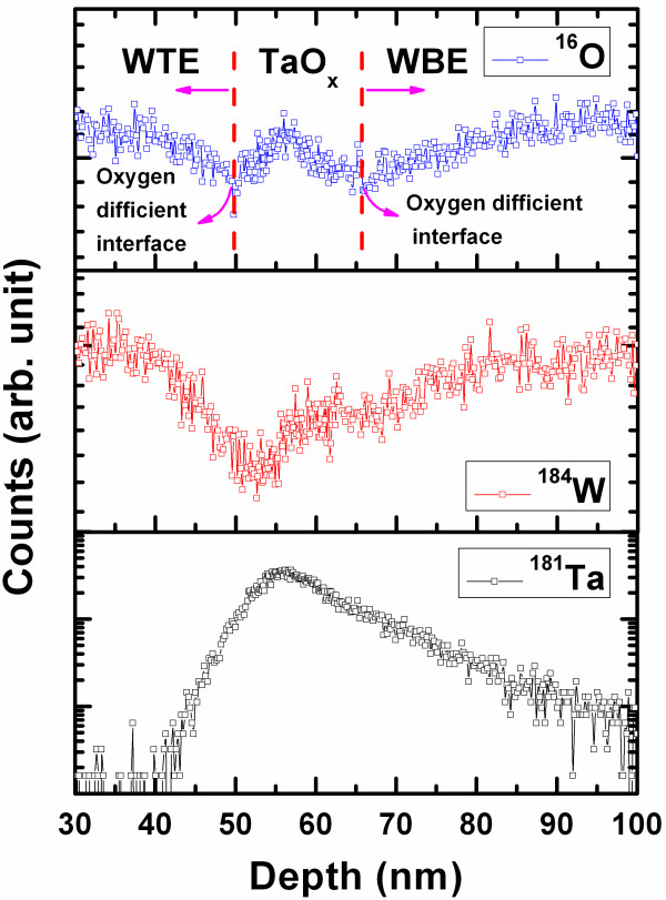
Figure 1a shows a typical cross-sectional TEM image of the W/TiOx/TaOx/W structure. The device size is 150 × 150 nm2. HRTEM images of the S2 and S1 devices are shown in Figure 1b,c. The thicknesses of the TiOx and TaOx layers are approximately 3 and 7 nm, respectively, and both films show an amorphous characteristic. The film deposited by rf sputtering is not a conformal deposition. Therefore, the TiOx layer can be seen clearly on outside and active regions of the via-hole (Figure 1a,c); however, this layer is no observed clearly on the sidewall of the via-hole. It is also obvious that the switching material on the sidewall is not necessary for switching properties of the RRAM devices because the electrons will find least path to move from TE to BE. This TiOx layer is also confirmed on outside and active region of the device by energy dispersive X-ray spectroscopy (not shown here). Figure 2 shows typical SIMS depth profiles of 16O, 184 W, and 181Ta materialsfor the S2 sample. The thickness of the TaOx layer is about 15 nm; however, this is higher than the deposited film thickness of 7 nm. This is due to the trail effect and surface roughness of W BE, as we can see from the depth of 57 to 65 nm (or approximately 7 nm) of the 184 W depth profile. The average surface roughness of 200-nm-thick W layer on SiO2/Si substrate is approximately 2.8 nm, which is observed by atomic force microscopy (AFM) with a scan area of 1 × 1 μm2, as shown in Figure 3. Therefore, the remaining thickness of approximately 4.2 nm (=7 to 2.8 nm) is coming from the trail effect of the SIMS depth profile. The depth from 50 to 57 nm is the thickness of TaOx layer, which is approximately 7 nm, as shown in Figure 2a,c. It is interesting to note that the TaOx/W interface is found to be an oxygen-deficient layer, which makes it a more conducting interface. On the other hand, the conducting filament will be formed after breaking the Ta-O bonds in the bulk Ta2O5 layer rather than the W/TaOx interface. This is because the Ta2O5 layer is more insulating than the W/TaOx interface, so the electric field will drop across the Ta2O5 film rather than the W/TaOx interface which probably results multi-filaments or an uncontrolled nanofilament diameter. As Ti removes oxygen from the Ta2O5 film in the W/TiOx/TaOx/W structure, the film becomes more oxygen-deficient TaOx, which is vital to achieve an improved resistive switching. Considering Gibbs, free energies of TiO2, Ta2O5, and WO3 films, which are −887.6, −760.5, and −506.5 kJ/mol, respectively, at 300 K [40], Ti will consume the highest oxygen content owing to its stronger reactivity than those of the other materials, thereby forming a Ta-rich (or defective TaOx) film. This also prevents oxidation of the W TE at the TaOx/W interface of device S1 owing to the migration of oxygen from the underlying films towards the Ti film, which contributes to the improved resistive switching memory performance as will be described.
Figure 1.
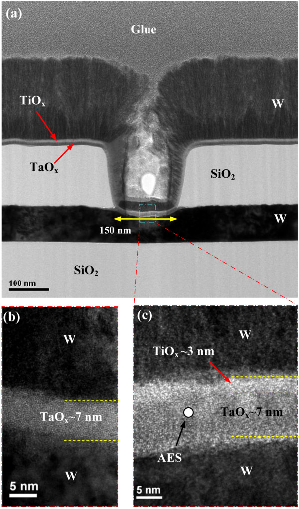
TEM and HRTEM images of W/TiOx/TaOx/W (S1) and W/TaOx/W (S2) structures. (a) TEM image of fabricated W/TiOx/TaOx/W (S1) structure. HRTEM images of (b) W/TaOx/W (S2) and (c) W/TiOx/TaOx/W (S1) structures.
Figure 2.
SIMS depth profile of W/TaO x /W (S2) structure.
Figure 3.
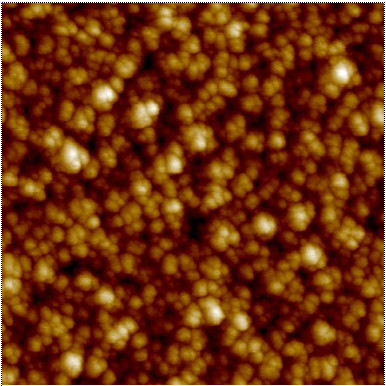
AFM image for surface roughness. The surface roughness of 200-nm-thick W layer on SiO2/Si substrate is approximately 2.8 nm.
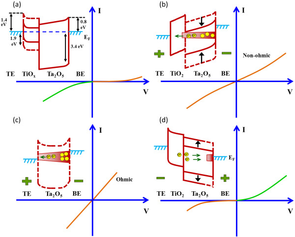
The leakage current values of most of the S1 pristine devices at a read voltage (Vread) of 1 V are higher than that of the S2 devices because of the presence of more oxygen vacancies in the TaOx layer owing to the oxygen-getter nature of the TiOx layer (Figure 4a). Typical current–voltage (I-V) curves (inset of Figure 4a) of both devices were asymmetrical with higher current at a negative voltage (≈281 pA for S1 and ≈ 12.6 pA for S2 at Vread = −1 V) compared with that measured at a positive voltage (≈9.8 pA for S1 and ≈ 0.6 pA for S2 at Vread = 1 V). This suggests that the W TE/TaOx interface has more oxygen vacancies than the TaOx/W BE interface, owing to oxygen migration towards W TE during deposition. The ideal leakage current is plotted in Figure 5a and is explained as follows: It is reported that the work function (Фm) of W and bandgap (Eg) of amorphous Ta2O5 and TiO2 are 4.55 [41], 4.2 [42], and 3.3 eV [43], respectively. The conduction band offsets of Ta2O5 and TiO2 with Si are 0.3 [44] and 0.9 eV [45], respectively. Taking the electron affinity of Si as 4.05 eV, the electron affinities of Ta2O5 and TiO2 are calculated to be 3.75 and 3.15 eV, respectively. The corresponding energy diagram is shown in Figure 5a as solid lines. Considering that the Eg of TiO2 for the pristine S1 device will be much lower because of oxygen vacancy creation during the deposition of W TE, the band diagram is shown in dotted lines (Figure 5a). In this case, electron injection dominates rather than hole injection because of a lower barrier height for electrons than for holes (0.8 to 1.4 vs. 3.4 eV). Both S1 and S2 devices show bipolar resistive switching behaviors. The S2 device shows few switching cycles with a higher leakage current of ≈ 10 μA at Vread = 1 V and a higher CC of 300 μA (Figure 4b). In this case, negatively charged oxygen ions (O2−) migrate from the switching material towards W TE, and this has a lesser possibility to form an oxygen-rich layer at the W TE/TaOx interface, leading to the formation of multi-conduction filaments. In the same way, no resistive switching is observed under negative forming voltage for either the S1 or S2 devices because oxygen ions migrate towards the W BE and permanent breakdown is observed (not shown here). The negative forming will lead to high switching current, which is similar to W/TaOx/W structure, and there is no oxygen-rich interfacial layer at the W/TaOx interface. This interfacial layer will have series resistance and protect from current overshoot effect. However, the insertion of a thin (≈3 nm) Ti layer in between the W and TaOx layers in the S1 device makes a vast difference because Ti can be used as an oxygen reservoir. Moreover, the S1 device exhibits >10,000 consecutive repeatable dc switching cycles with a better resistance ratio of 102 under a low CC of 80 μA (Figure 4c). The transport mechanism follows the trap-charge-controlled space charge limited current conduction (not shown here). However, a thicker Ti layer (5 nm) results in unstable switching cycles because it gets more oxygen and behaves as an insulating layer. This may lead to the conducting filament formation/rupture in the TiOx layer rather than the TaOx layer. It is reported that the TiO2 switching layer has magneli phase and the memory window is collapsed after few cycles [46]. That is the reason to have unstable switching using thicker (5 nm) Ti interracial layer. Therefore, thickness optimization is very important and we have chosen those thicknesses of TaOx and TiOx layers here. The thinnest Ti layer of <3 nm is also not to be used because of direct current flow through this layer. Therefore, the thinner (3 nm) Ti layer will control the current overflow as well as will control the filament diameter. The yield of the S1 device is very high (>95%), while that of the S2 device is very low (approximately 10%). In addition, the S2 device cannot be switched below a CC of 300 μA and shows an ohmic behavior, while the S1 device shows switching even at a low CC of 10 μA (discussed later) with non-ohmic current conduction. The average values and standard deviation/average are found to be 39.7 and 0.11, 38.4 kΩ and 0.08 for low-resistance state (LRS) and 1.9 and 2.11, 8.6 MΩ and 0.43, for high-resistance state (HRS) at Vread of 1 V and −1 V, respectively (Figure 4d). This suggests that the LRS has a tighter distribution than the HRS because of the formation of the TiO2 layer, which will have a higher Eg than the pristine one. Similarly, the leakage current at Vread of −1 V is lower than that at +1 V because of the lower electron injection barrier at the TE/TiO2 interface than that at the BE/TaOx interface after switching. Under ‘SET’, O2− will migrate from TaOx towards the TE, resulting in a TiO2 layer which controls the conducting vacancy filament diameter in the TaOx layer by controlling current overflow and producing a tighter distribution of the LRS. Owing to this series resistance, the S1 devices exhibit non-ohmic-simulated (or nonlinear) ideal current, as shown in Figure 5b, whereas an ohmic current is observed for the S2 devices under SET (Figure 5c). It is true that the conducting filament is formed through the TaOx film (Figure 5b,c), which is also confirmed by AES spectra of the TaOx film for pristine and afterswitching of the TaOx-based devices (Figure 6). The differentiated counts with respect to kinetic energy (dC/dE) versus kinetic energy (E) are plotted. The spectrum positions are in the middle of the TaOx switching layer with a typical device size of 0.4 × 0.4 μm2. Different RRAM devices of pristine and switching were used to get the AES spectra. Even though different devices were used, the spectra of both the pristine (blue open square symbols) and switched (yellow solid triangle symbols) devices were maintained from the same depth. Ta-MN (1,737 and 1,680 eV) and O-KL (468, 483, and 503 eV) are observed, which confirms the formation of a TaOx layer. The atomic percentages of Ta-MN3 and O-KL1 are 37.38% and 62.62% for the pristine device and 44.69% and 55.31% for the switched device, respectively. It is believed that the spectra difference is not a variation, and the oxygen ion migration from the TaOx switching layer. Due to a small amount of oxygen migration, the difference of the two spectra will be small. The atomic percentages were calculated by using commercial software for AES spectra. Basically, this decrease in oxygen content and increase in Ta content after switching is of the evidence that an oxygen-deficient filament is formed owing to oxygen ion migration as well as the lower energy gap of the TaOx layer, as shown by the dotted line in Figure 5b. When negative voltage is applied to the TE, oxygen ions are pushed from the TiO2 layer towards the conducting filament where they recombine with oxygen vacancies or oxidize the conducting filament. The device will be in HRS (Figure 5d). Control of oxygen-deficient filament formation and rupture is facilitated by insertion of the thin Ti layer at the TE/TaOx interface, which results in repeatable and reproducible resistive switching characteristics.
Figure 4.
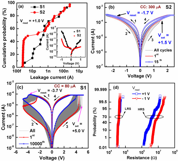
Cumulative probabilities of leakage currents and LRS/HRS and switchingI-Vcurves of S1 and S2. (a) Cumulative probability of leakage currents for S1 and S2 devices with typical via size of 0.8 μm. Inset: leakage current vs. voltage characteristics. Switching I-V curves of (b) S2 and (c) S1 devices. The S2 device shows instability after a few cycles, while 10,000 consecutive switching cycles are observed for the S1 device. (d) Cumulative probability of LRS and HRS under Vread of ±1 V for the S1 devices.
Figure 5.
Schematic illustration of switching mechanism using simple energy band diagrams withI-Vcharacteristics. (a) Energy bands of pristine S1 structure device and ideal leakage current. For TiO2, the solid line is due to the smaller energy gap of the defective TiOx film. I-V of LRS and corresponding energy bands with conducting filaments for (b) S1 and (c) S2 devices. For TaOx, the solid line is due to the lower energy gap caused by the presence of oxygen-deficient filament. The S1 devices show non-ohmic I-V due to TiO2 layer formation at the W/TaOx interface. (d) Filament oxidation and leakage current at HRS are shown for the W/TiOx/TaOx/W devices. Filament formation/rupture is controlled by the TiO2 layer due to O2− ion migration.
Figure 6.
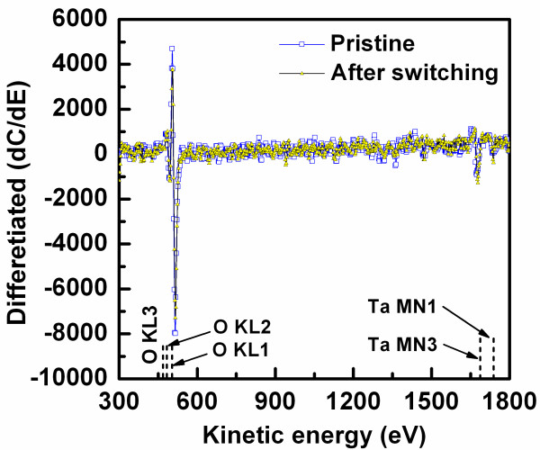
Differentiated counts with respect to kinetic energy (dC/dE). AES spectra vs. kinetic energy for pristine and after-switching RRAM devices. The spectra are from a typical via size of 0.4 × 0.4 μm2 and measured inside the middle of via regions (open blue square symbols for pristine and yellow solid triangle symbols for switched devices). An oxygen-deficient TaOx layer is observed after few switching cycles, confirming oxygen-deficient TaOx filament formation after SET.
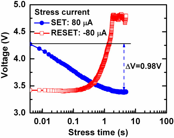
The conducting filament diameter is estimated using a new method under a constant current stress of 80 μA (Figure 7). The voltage decreases (or increases) under positive (or negative) current stress after a SET (or RESET) operation. First, it is considered as a parallel plate metal-insulator-metal (MIM) capacitor. Under external constant current stress, the Ta-O bonds breaks and creates the defects due to oxygen ion migration, which results a reducing voltage across the capacitor. The captured crosssection of the defects will lead to the diameter of the conducting filament. Assuming a single cylindrical nanofilament, the diameter (D) under SET can be estimated as [47]
Figure 7.
Voltage shift vs. stressing time under a current of ±80 μA for SET/RESET operations. The conducting filament diameter is calculated to be approximately 3 nm.
| (1) |
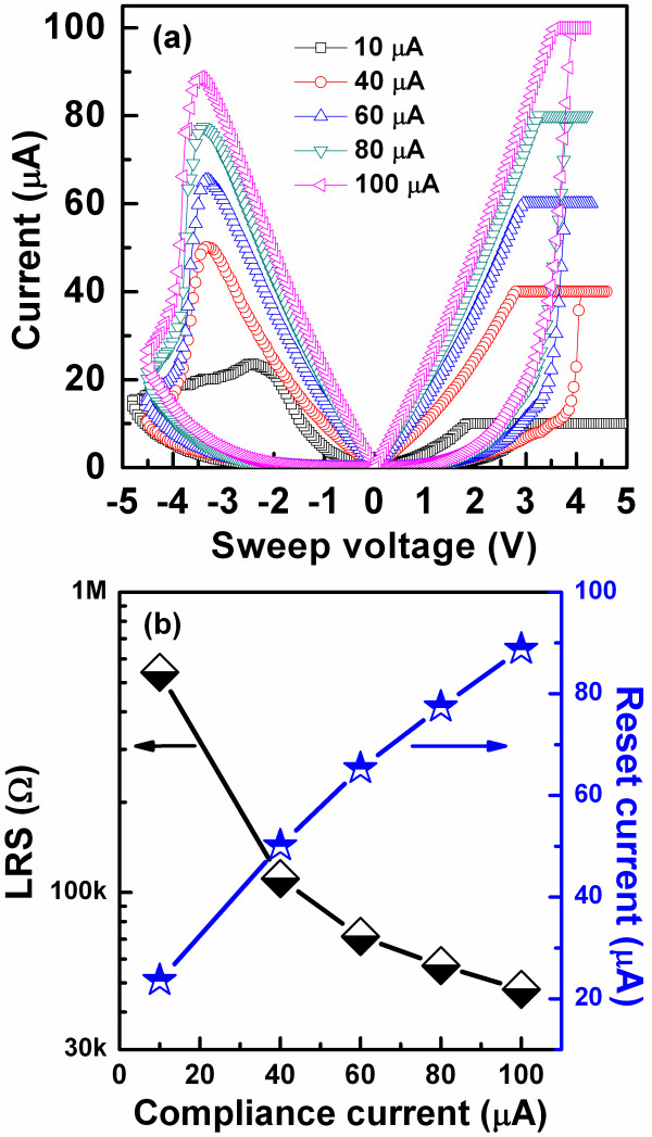
where ΔV (changes in the voltage shift under SET and RESET) is found to be 0.98 V (Figure 7), q is the electronic charge (1.602 × 10⁻¹⁹ C), and is the dielectric permittivity of amorphous Ta2O5 film ( ≈20 to 25). Considering all values in Equation 1, the diameter of the nanofilament is approximately 2.9 to 2.6 nm. This suggests that the present resistive switching memory device can be scaled down to <3 nm. Previously reported diameters of 5 to 10 nm for Pt/TiO2/Pt [12], ≈15 nm for Ti/Fe:SrTiO3/Nb:SrTiO3[42], and ≈ 1,000 nm for Pt/CuO/Pt [48] are slightly closer and higher than our calculated values, likely owing to the use of different structures as well as materials. Further study may be needed to clearly understand these results. Figure 8a shows the resistive switching characteristics with different CCs from 10 to 100 μA. The low-resistance state decreases with increasing CCs from 10 to 100 μA (Figure 8a,b), which will be useful for multi-level data storage applications. As the filament diameter increases with higher CCs, the low-resistance state decreases, and the value of RESET voltage increases. The RESET current can be scaled down to 23 μA at a low CC of 10 μA, which will be useful to a low-power operation RRAM in the near future. Our novel device also has a long read pulse endurance of >105 cycles (Figure 9a) and excellent data retention of >104 s with a good resistance ratio of >102 at 85°C at a low CC of 80 μA (Figure 9b). The HRS is slightly decreased with longer elapsed time; however, it is still high, approximately 10 MΩ. Further study is needed to clarify this issue. A data retention of >103 s is also observed for a low CC of 10 μA (not shown here). This RRAM device shows good program erase endurance of >1,000 cycles with a pulse width of 500 μs (Figure 9c). Considering the obtained nanofilament diameter of approximately 3 nm, a high-density (≈100 Tbit/in.2) nanoscale nonvolatile memory can be achievable in the future.
Figure 8.
I-Vhysteresis characteristics (a) LRS and RESET currents (b) with 10- to 100-μA CCs. A device could be operated with a low RESET current of 23 μA.
Figure 9.
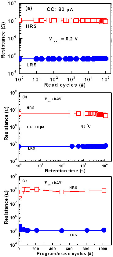
Long pulse endurance and good data retention. (a) Long read pulse endurance of >105cycles and (b) good data retention of >104 s with a good resistance ratio of >102 at 85°C are obtained at a low CC of 80 μA. (c) Program/erase endurance of >1,000 cycles with a pulse width of 500 μs.
Conclusions
Improvement in resistive switching performance, particularly 10,000 consecutive switching cycles with tight distribution in LRS/HRS of >102, long read pulse endurance of >105, and good data retention of 104 s at 85°C, has been achieved under a low CC of 80 μA by exploiting the oxygen-getter nature of a Ti nanolayer in a W/TiOx/TaOx/W structure. A small device of 150 × 150 nm2 and a defective TaOx film are confirmed by TEM. O2− ion migration because of lower barrier height for electrons leads to a switching mechanism based on filament formation/rupture. The presence of controllable oxygen-deficient TaOx nanofilament after switching has been investigated by AES. Furthermore, the device could be operated with a small RESET current of 23 μA. A small nanofilament diameter of 3 nm under a low CC of 80 μA has been calculated using a new method, which has a high memory density of ≈ 100 Tbit/in.2, expected to be very useful for future sub-10-nm applications.
Competing interests
The authors declare that they have no competing interests.
Authors’ contributions
AP carried out this research work under the instruction of SM. Fabrication process was also instructed by HCC and CSL. AES spectra were taken by TCT under the instruction of SM. All authors read and approved the final manuscript.
Contributor Information
Amit Prakash, Email: amit.knp02@gmail.com.
Siddheswar Maikap, Email: sidhu@mail.cgu.edu.tw.
Hsien-Chin Chiu, Email: hcchiu@mail.cgu.edu.tw.
Ta-Chang Tien, Email: tien@itri.org.tw.
Chao-Sung Lai, Email: cslai@mail.cgu.edu.tw.
Acknowledgments
This work was supported by the National Science Council (NSC), Taiwan, under contract numbers NSC-98-2221-E-182-052-MY3, NSC-101-2221-E-182-061, and NSC-102-2221-E-182-057-MY2. The authors are grateful to the Electronic and Optoelectronic Research Laboratories, Industrial Technology Research Institute, Hsinchu, Taiwan for their support on W bottom electrode pattern.
References
- Waser R, Dittmann R, Staikov G, Szot K. Redox-based resistive switching memories - nanoionic mechanisms, prospects, and challenges. Adv Mater. 2009;9:2632. doi: 10.1002/adma.200900375. [DOI] [PubMed] [Google Scholar]
- Sawa A. Resistive switching in transition metal oxides. Mater Today. 2008;9:28. [Google Scholar]
- Liu Q, Sun J, Lv H, Long S, Yin K, Wan N, Li Y, Sun L, Liu M. Real-time observation on dynamic growth/dissolution of conductive filaments in oxide-electrolyte-based ReRAM. Adv Mater. 1844;9:24. doi: 10.1002/adma.201104104. [DOI] [PubMed] [Google Scholar]
- Sato Y, Kinoshita K, Aoki M, Sugiyama Y. Reduction in the reset current in a resistive random access memory consisting of NiOx brought about by reducing a parasitic capacitance. Appl Phys Lett. 2007;9:033503. doi: 10.1063/1.2431792. [DOI] [Google Scholar]
- Lee MJ, Lee CB, Lee D, Lee SR, Chang M, Hur JH, Kim YB, Kim CJ, Seo DH, Seo S, Chung UI, Yoo IK, Kim K. A fast, high-endurance and scalable non-volatile memory device made from asymmetric Ta2O(5−x)/TaO(2−x) bilayer structures. Nat Mater. 2011;9:625. doi: 10.1038/nmat3070. [DOI] [PubMed] [Google Scholar]
- Yoon J, Choi H, Lee D, Park JB, Lee J, Seong DJ, Ju Y, Chang M, Jung S, Hwang H. Excellent switching uniformity of Cu-doped MoOx/GdOx bilayer for nonvolatile memory applications. IEEE Electron Device Lett. 2009;9:457. [Google Scholar]
- Prakash A, Maikap S, Lai CS, Lee HY, Chen WS, Chen F, Kao MJ, Tsai MJ. Improvement uniformity of resistive switching parameters by selecting the electroformation polarity in IrOx/TaOx/WOx/W structure. Jpn J Appl Phys. 2012;9:04DD06. doi: 10.7567/JJAP.51.04DD06. [DOI] [Google Scholar]
- Banerjee W, Maikap S, Lai CS, Chen YY, Tien TC, Lee HY, Chen WS, Chen FT, Kao MJ, Tsai MJ, Yang JR. Formation polarity dependent improved resistive switching memory characteristics using nanoscale (1.3 nm) core-shell IrOx nano-dots. Nanoscale Res Lett. 2012;9:194. doi: 10.1186/1556-276X-7-194. [DOI] [PMC free article] [PubMed] [Google Scholar]
- Yoon JH, Kim KM, Lee MH, Kim SK, Kim GH, Song SJ, Seok JY, Hwang CS. Role of Ru nano-dots embedded in TiO2 thin films for improving the resistive switching behavior. Appl Phys Lett. 2010;9:232904. doi: 10.1063/1.3525801. [DOI] [Google Scholar]
- Lee HY, Chen PS, Liu WH, Wang SM, Gu PY, Hsu YY, Tsai CH, Chen WS, Chen F, Tsai MJ, Lien C. Robust high-resistance state and improved endurance of HfOx resistive memory by suppression of current overshoot. IEEE Electron Device Lett. 2011;9:1585. [Google Scholar]
- Choi BJ, Jeong DS, Kim SK, Rohde C, Choi S, Oh JH, Kim HJ, Hwang CS, Szot K, Waser R, Reichenberg B, Tiedke S. Resistive switching mechanism of TiO2 thin films grown by atomic-layer deposition. J Appl Phys. 2005;9:033715. doi: 10.1063/1.2001146. [DOI] [Google Scholar]
- Kwon DH, Kim KM, Jang JH, Jeon JM, Lee MH, Kim GH, Li XS, Park GS, Lee B, Han S, Kim M, Hwang CS. Atomic structure of conducting nanofilaments in TiO2 resistive switching memory. Nat Nanotechnol. 2010;9:148. doi: 10.1038/nnano.2009.456. [DOI] [PubMed] [Google Scholar]
- Lee SR, Char K, Kim DC, Jung R, Seo S, Li XS, Park GS, Yoo IK. Resistive memory switching in epitaxially grown NiO. Appl Phys Lett. 2007;9:202115. doi: 10.1063/1.2815658. [DOI] [Google Scholar]
- Long S, Cagli C, Ielmini D, Liu M, Sune J. Reset statistics of NiO-based resistive switching memories. IEEE Electron Device Lett. 2011;9:1570. [Google Scholar]
- Long S, Cagli C, Ielmini D, Liu M, Sune J. Analysis and modeling of resistive switching statistics. J Appl Phys. 2012;9:074508. doi: 10.1063/1.3699369. [DOI] [Google Scholar]
- Yu S, Guan X, Wong HSP. Conduction mechanism of TiN/HfOx/Pt resistive switching memory: a trap-assisted-tunneling model. ApplPhys Lett. 2011;9:063507. doi: 10.1063/1.3624472. [DOI] [Google Scholar]
- Chen YY, Goux L, Clima S, Govoreanu B, Degraeve R, Kar GS, Fantini A, Groeseneken G, Wouters DJ, Jurczak M. Endurance/retention trade-off on HfO2/metal cap 1T1R bipolar RRAM. IEEE Trans Electron Devices. 2013;9:1114. [Google Scholar]
- Long S, Lian X, Ye T, Cagli C, Perniola L, Miranda E, Liu M, Sune J. Cycle-to-cycle intrinsic RESET statistics in HfO2-based unipolar RRAM devices. IEEE Electron Device Lett. 2013;9:623. [Google Scholar]
- Lin CY, Wu CY, Wu CY, Lee TC, Yang FL, Hu C, Tseng TY. Effect of top electrode material on resistive switching properties of ZrO2 film memory devices. IEEE Electron Device Lett. 2007;9:366. [Google Scholar]
- Guan W, Long S, Jia R, Liu M. Nonvolatile resistive switching memory utilizing gold nanocrystals embedded in zirconium oxide. Appl Phys Lett. 2007;9:062111. doi: 10.1063/1.2760156. [DOI] [Google Scholar]
- Liu Q, Guan W, Long S, Liu M, Zhang S, Wang Q, Chen J. Resistance switching of Au-implanted-ZrO2 film for nonvolatile memory application. J Appl Phys. 2008;9:114514. doi: 10.1063/1.3033561. [DOI] [Google Scholar]
- Liu Q, Guan W, Long S, Jia R, Liu M, Chen J. Resistive switching memory effect of ZrO2 films with Zr+ implanted. Appl Phys Lett. 2008;9:012117. doi: 10.1063/1.2832660. [DOI] [Google Scholar]
- Guan W, Long S, Liu Q, Liu M, Wang W. Nonpolar nonvolatile resistive switching in Cu doped ZrO2. IEEE Electron Device Lett. 2008;9:434. [Google Scholar]
- Wang SY, Lee DY, Tseng TY, Lin CY. Effects of Ti top electrode thickness on the resistive switching behaviors of rf-sputtered ZrO2 memory films. Appl Phys Lett. 2009;9:112904. doi: 10.1063/1.3231872. [DOI] [Google Scholar]
- Wang SY, Lee DY, Huang TY, Wu JW, Tseng TY. Controllable oxygen vacancies to enhance resistive switching performance in a ZrO2-based RRAM with embedded Mo layer. Nanotechnology. 2010;9:495201. doi: 10.1088/0957-4484/21/49/495201. [DOI] [PubMed] [Google Scholar]
- Li Y, Long S, Lv H, Liu Q, Wang Y, Zhang S, Lian W, Wang M, Zhang K, Xie H, Liu S, Liu M. Improvement of resistive switching characteristics in ZrO2 film by embedding a thin TiOx layer. Nanotechnology. 2011;9:254028. doi: 10.1088/0957-4484/22/25/254028. [DOI] [PubMed] [Google Scholar]
- Lin CC, Chang YP, Lin HB, Lin CH. Effect of non-lattice oxygen on ZrO2-based resistive switching memory. Nanoscale Res Lett. 2012;9:187. doi: 10.1186/1556-276X-7-187. [DOI] [PMC free article] [PubMed] [Google Scholar]
- Zhang T, Zhang X, Ding L, Zhang W. Study on resistance switching properties of Na0.5Bi0.5TiO3 thin films using impedance spectroscopy. Nanoscale Res Lett. 2009;9:1309. doi: 10.1007/s11671-009-9397-4. [DOI] [PMC free article] [PubMed] [Google Scholar]
- Sun X, Li G, Chen L, Shi Z, Zhang W. Bipolar resistance switching characteristics with opposite polarity of Au/SrTiO3/Ti memory cells. Nanoscale Res Lett. 2011;9:599. doi: 10.1186/1556-276X-6-599. [DOI] [PMC free article] [PubMed] [Google Scholar]
- Chiu FC, Li PW, Chang WY. Reliability characteristics and conduction mechanisms in resistive switching memory devices using ZnO thin films. Nanoscale Res Lett. 2012;9:178. doi: 10.1186/1556-276X-7-178. [DOI] [PMC free article] [PubMed] [Google Scholar]
- Peng CN, Wang CW, Chan TC, Chang WY, Wang YC, Tsai HW, Wu WW, Chen LJ, Chueh YL. Resistive switching of Au/ZnO/Au resistive memory: anin situobservation of conductive bridge formation. Nanoscale Res Lett. 2012;9:559. doi: 10.1186/1556-276X-7-559. [DOI] [PMC free article] [PubMed] [Google Scholar]
- Rahaman SZ, Maikap S, Chen WS, Lee HY, Chen FT, Kao MJ, Tsai MJ. Repeatable unipolar/bipolar resistive memory characteristics and switching mechanism using a Cu nanofilament in a GeOx film. Appl Phys Lett. 2012;9:073106. doi: 10.1063/1.4745783. [DOI] [PMC free article] [PubMed] [Google Scholar]
- Syu YE, Chang TC, Tsai TM, Chang GW, Chang KC, Lou JH, Tai YH, Tsai MJ, Wang YL, Sze SM. Asymmetric carrier conduction mechanism by tip electric field in WSiOx resistance switching device. IEEE Electron Device Lett. 2012;9:342. [Google Scholar]
- Rahaman SZ, Maikap S, Tien TC, Lee HY, Chen WS, Chen F, Kao MJ, Tsai MJ. Excellent resistive memory characteristics and switching mechanism using a Ti nanolayer at the Cu/TaOx interface. Nanoscale Res Lett. 2012;9:345. doi: 10.1186/1556-276X-7-345. [DOI] [PMC free article] [PubMed] [Google Scholar]
- Prakash A, Maikap S, Lai CS, Tien TC, Chen WS, Lee HY, Chen FT, Kao MJ, Tsai MJ. Bipolar resistive switching memory using bilayer TaOx/WOx films. Solid State Electron. 2012;9:35. [Google Scholar]
- Chen C, Song C, Yang J, Zeng F, Pan F. Oxygen migration induced resistive switching effect and its thermal stability in W/TaOx/Pt structure. Appl Phys Lett. 2012;9:253509. doi: 10.1063/1.4730601. [DOI] [Google Scholar]
- Terai M, Sakotsubo Y, Kotsuji S, Hada H. Resistance Controllability of Ta2O5/TiO2 stack ReRAM for low-voltage and multilevel operation. IEEE Electron Device Lett. 2010;9:204. [Google Scholar]
- Ninomiya T, Wei Z, Muraoka S, Yasuhara R, Katayama K, Takagi T. Conductive filament scaling of TaOx bipolar ReRAM for improving data retention under low operation current. IEEE Trans Electron Devices. 2013;9:1384. [Google Scholar]
- Wei Z, Kanzawa Y, Arita K, Katoh Y, Kawai K, Muraoka S, Mitani S, Fujii S, Katayama K, Iijima M, Mikawa T, Ninomiya T, Miyanaga R, Kawashima Y, Tsuji K, Himeno A, Okada T, Azuma R, Shimakawa K, Sugaya H, Takagi T, Yasuhara R, Horiba K, Kumigashira H, Oshima M. Highly reliable TaOx ReRAM and direct evidence of redox reaction mechanism. Tech Dig - Int Electron Devices Meet. 2008;9:293. [Google Scholar]
- The interactive Ellingham diagram. http://www.doitpoms.ac.uk/tlplib/ellingham_diagrams/interactive.php.
- Michaelson HB. The work function of the elements and its periodicity. J Appl Phys. 1977;9:4729. doi: 10.1063/1.323539. [DOI] [Google Scholar]
- Stille S, Lenser C, Dittmann R, Koehl A, Krug I, Muenstermann R, Perlich J, Schneider CM, Klemradt U, Waser R. Detection of filament formation in forming-free resistive switching SrTiO3 devices with Ti top electrodes. Appl Phys Lett. 2012;9:223503. doi: 10.1063/1.4724108. [DOI] [Google Scholar]
- Aarik J, Aidla A, Kiisler AA, Uustare T, Sammelselg V. Effect of crystal-structure on optical-properties of TiO2 films grown by atomic layer deposition. Thin Solid Films. 1997;9:270. doi: 10.1016/S0040-6090(97)00135-1. [DOI] [Google Scholar]
- Gu D, Li J, Dey SK, Waard HD, Marcus S. Nanochemistry, nanostructure, and electrical properties of Ta2O5 film deposited by atomic layer deposition and plasma-enhanced atomic layer deposition. J Vac Sci Technol B. 2006;9:2230. doi: 10.1116/1.2335432. [DOI] [Google Scholar]
- Maikap S, Wang TY, Tzeng PJ, Lin CH, Tien TC, Lee LS, Yang JR, Tsai MJ. Band offsets and charge storage characteristics of atomic layer deposited high-kHfO2/TiO2 multilayers. Appl Phys Lett. 2007;9:262901. doi: 10.1063/1.2751579. [DOI] [Google Scholar]
- Yang JJ, Zhang MX, Strachan JP, Miao F, Pickett MD, Kelley RD, Medeiros-Ribeiro G, Williams RS. High switching endurance in TaOx memristive devices. Appl Phys Lett. 2010;9:232102. doi: 10.1063/1.3524521. [DOI] [Google Scholar]
- Prakash A, Maikap S, Rahaman SZ, Majumdar S, Manna S, Ray SK. Resistive switching memory characteristics of Ge/GeOx nanowires and evidence of oxygen ion migration. Nanoscale Res Lett. 2013;9:220. doi: 10.1186/1556-276X-8-220. [DOI] [PMC free article] [PubMed] [Google Scholar]
- Yasuhara R, Fujiwara K, Horiba K, Kumigashira H, Kotsugi M, Oshima M, Takagi H. Inhomogeneous chemical states in resistance-switching devices with a planar-type Pt/CuO/Pt structure. Appl Phys Lett. 2009;9:012110. doi: 10.1063/1.3175720. [DOI] [Google Scholar]


