Abstract
The ability to accurately design carbon nanofibre (CN) field emitters with predictable electron emission characteristics will enable their use as electron sources in various applications such as microwave amplifiers, electron microscopy, parallel beam electron lithography and advanced Xray sources. Here, highly uniform CN arrays of controlled diameter, pitch and length were fabricated using plasma enhanced chemical vapour deposition and their individual emission characteristics and field enhancement factors were probed using scanning anode field emission mapping. For a pitch of 10 µm and a CN length of 5 µm, the directly measured enhancement factors of individual CNs was 242, which was in excellent agreement with conventional geometry estimates (240). We show here direct empirical evidence that in regular arrays of vertically aligned CNs the overall enhancement factor is reduced when the pitch between emitters is less than half the emitter height, in accordance to our electrostatic simulations. Individual emitters showed narrow Gaussian-like field enhancement distributions, in excellent agreement with electric field simulations.
Carbon nanotubes and nanofibres (CNs); highly-conductive high-aspect ratio graphitic carbon allotropes, have attracted immense interest for field emission applications over the past decade1,2,3,4,5. Their resilience towards electromigration and their ability to carry higher current densities than conventional materials coupled with their rapid response time and low driving voltages make them ideal candidates for various electron emission applications, such as micro X-ray sources6,7, microwave amplifiers8, travelling wave tubes9, ultra-high resolution electron microscopy6, and highly-parallel electron beam lithography micro-gun systems10,11. Conventional refractory metal emitters, such as chemically etched W tips, or Spindt-like emitters often have poorly defined tips with low aspect ratios and poor tip-to-tip reproducibility, making it difficult to predict their emission characteristics accurately, whilst cold cathode electron emitters with engineered field enhancement factors and deterministic electron emission characteristics have been hitherto unmanufacturable en masse due to difficulties in achieving high process uniformity during fabrication. Extremely uniform arrays of CNs12 offer many advantages. Such vertically aligned CNs have near-ideal whisker-like shapes with hemispherical tips, where the tip radius is controlled by the metal catalyst which nucleates the CN growth. Moreover, the position and pitch of the CN are determined by simple matured lithographic techniques.
Here we present direct scanning anode field emission mapping measurements detailing the field enhancement factor distribution from highly uniform arrays of CNs of varying pitch through which we assess the accuracy of simple geometric arguments in determining the field enhancement factor of individual CNs and arrays of CNs. Individual CNs show field enhancement factors that are in excellent agreement with estimates based on the emitter geometry and ab initio electrostatics simulations. We have developed empirical models which incorporate the implicit axial and interfacial resistances of each CN as well as the typical breakdown currents, based on measured field enhancement factor distributions which we employ to deterministically predict the emission profiles of our CN arrays.
Experimental
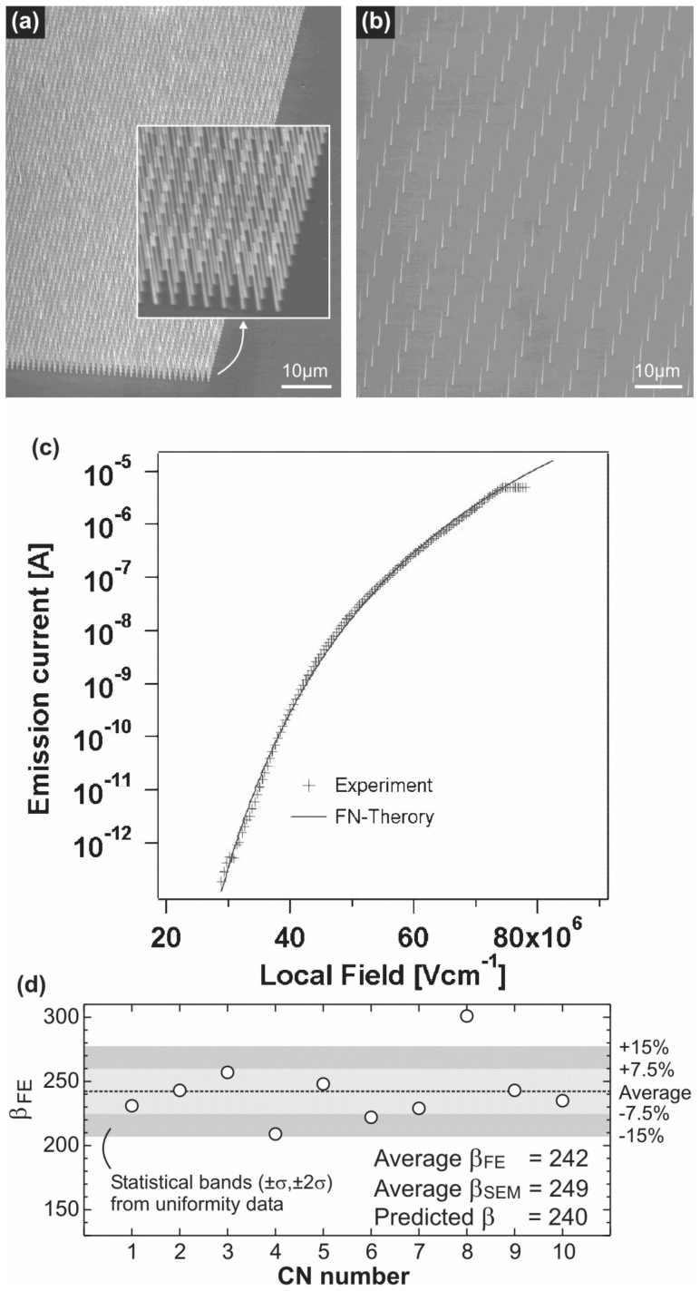
Scanning electron micrographs of individual vertically aligned CN arrays of pitch 1 μm and 5 μm, are shown in Figures 1(a) and (b). CNs were grown by plasma enhanced chemical vapor deposition, as reported in further detail elsewhere12,13 (see Methods). Individual CNs had a mean (±1σ) radius of 24.5 nm (4.1%) and a mean length of 5.8 μm (6.3%). It has been shown that for whisker-like geometries the emitter field enhancement factor is approximately given by the aspect ratio, h/r, where h is the emitter height and r is the emitter radius. In this case, for a single perfectly isolated emitter, βemitter = 240 (pitch→∞), with an estimated standard deviation of approximately 18 (7.5%) by linear combination of errors. We have directly measured βemitter on 10 individual CNs, at a pitch of 25 µm, using scanning anode field emission microscopy (SAFEM) to assess the spatial reproducibility of the emitters. The measured field enhancement factors extracted from 10 individual CNs, at a pitch of 25 μm, showed that the mean (±1σ) field enhancement factor of individual emitters was 242 (±18), agreeing extremely well with our earlier geometric predictions (Figure 1(d)) and suggesting that for pitches greater than twice the emitter height the array field enhancement factor is well estimated by the aspect ratio of the vertically aligned emitter. All CNs were first conditioned by a constant current scan at 10 µA to drive off weakly bound surface absorbates. The emitter locations were determined by an 11 nA constant current scan at a fixed anode-cathode separation and locating the voltage minima in the V(x, y) map. Individual emitters were resolvable with the spacing between voltage minima corresponding to the patterned emitter spacing. The scanning anode was then situated directly above a given emitter and an I-V ramp performed, as shown in Figure 1(c). The Fowler-Nordheim (FN) plots were extracted assuming a work function of 4.9 eV(graphitic C). The measurements have been expressed in terms of the emission current and the local electric field (Elocal), where the spatially resolved field enhancement factor β(x, y) = Elocal/Eapl (x, y) = Elocal/kV(x, y). Here k is an empirically determined constant. In the case of the measured emitters k = 0.0624 (μm)−1. β(x, y) is directly accessible for all emitters by measuring the constant current V(x, y) map. Contrary to prior studies, in the case of a single emitter, formed from a quasi-metallic bamboo like CN, the measured I-V plot shows an excellent fit with the traditional FN approximation14, for an approximate single tip emission area of 6 × 10⁻¹¹ cm2, as shown in Figure 1(c). We find that typical individual emitter breakdown occurred at ~3 µA.
Figure 1.
Scanning electron micrographs of uniform CN arrays with pitches of (a) 1 µm and (b) 5 µm (Scale bar: 10 µm). (c) Typical FE characteristics of a CN showing an excellent fit with FN theory for a 5 µm pitch array. (d) Variation in the field enhancement factor, βFE, for 10 individual CNs at a pitch of 5 µm sowing a mean of 242 that is close to the predicted β ( = 240) inferred from the emitter geometry estimates. ±σ (7.5%) and ±2σ (15%) bands as illustrated.
Results and Discussion
FN theory has been widely adopted for a wide variety of field emission materials. However, it is based on the free-electron model and has proven only truly valid for electron-dense metallic emitters5,15. CN ensembles have been shown previously to deviate from this model, particularly in the high field regime16,17,18. For the arrays considered here the total emission current density, J, is derived by spatially integrating the emission current over entire array, such that;
 |
where A = 1.56 × 10⁻⁶ A V−2 eV, B = 6.83 × 10⁹ V eV−3/2 V m−1, and ϕ is the work function of the emitter. β(x, y) is the spatially varying field enhancement factor, d is the anode-cathode separation (m) and V is the applied voltage (V). However, this approach does not facilitate direct emitter engineering as it requires prior knowledge of each individual emitters dimensions in order to assess β(x, y), often by time-consuming inspection via electron microscopy. Moreover, the field enhancement factor of the array is only approximated by the individual emitter aspect ratio making this approach increasingly inaccurate for disordered nanostructured thin films. Here we present direct empirical evidence for the detailed relationship between the emitter aspect ratio and pitch and assess the validity and accuracy of simple geometric approaches to direct measurement.
Field enhancement distributions
Direct measurement of β for large ensembles of CNs allows us to derive a field enhancement distribution, f(β), which when integrated over the number density of a particular array gives an increasingly accurate representation of the emission performance relative to conventional parallel plate measurements. Thus, if the variation in β of individual CNs is known a priori then it is possible to determine the complete response of any designed array in a deterministic fashion allowing us to precisely predict emission profiles (i.e. maximum emission current density, turn-on potential, threshold potential, and βarray) as we demonstrate here.
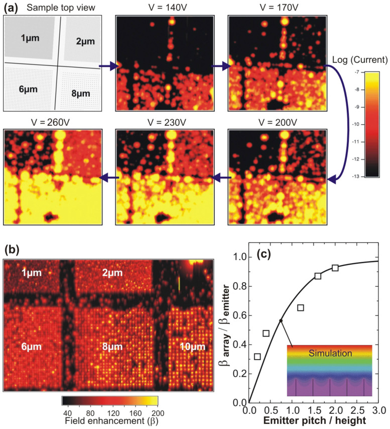
SAFEM measurements19 of arrays with pitches of 1, 2, 6, 8 and 10 µm fabricated on a single substrate are shown in Figure 2(a). The extraction bias was sequentially incremented from 140 V to 260 V (ΔV = 30 V). Individual emitters were resolved with extremely high spatial accuracy, with more than 90% showing electron emission within this voltage range. The applied electric field, Eapl was determined by performing a constant current measurement at a fixed separation, and then increasing the anode-sample separation by Δz and repeating the measurement. During this second measurement the applied bias was increased by ΔV, in order to liberate a current of equal magnitude to that of the initial scan. Thus, ΔV/Δz gives a direct measure of Eapl thereby giving empirical access to the field enhancement factor without having accurate knowledge of the absolute initial height of the SAFEM anode. In this way we have directly measured the field enhancement factors of > 103 individual vertically aligned CNs.
Figure 2.
(a) Schematic showing CN arrays of various pitch (1, 2, 6 and 8 µm) grown on a single substrate with the corresponding SAFEM current maps at extraction potentials of 140, 170, 200, 230, 260 V. Scans were performed with a constant emission current of 11 nA and a separation of 7 µm. The 6 μm and 8 μm pitch arrays emit more than two orders of magnitude more current (per emitter) than the 1 μm and 2 μm pitch arrays. A linear array separates each disparate CN pitch zone and this accounts for the observed emission current at the boundaries between each pitch area. (b) A typical β map for 1, 2, 6, 8, and 10 µm pitch CN arrays. (c) Theoretical and measured (□) variation in βarray/βemitter as a function of emitter pitch-to-height ratio. The CN height was ~5 µm and the apparent field enhancement factor was assumed to be ~300. The slightly larger βemitter used here, compared to the ~250 for individual CNs, was principally due to a measurement artifact. The inset illustrates the potential distribution highlighting the current limiting effects of nearest neighbor electro-static shielding for a CN height/radius of 5 μm/25 nm, an applied electric field of 1 V/μm and a potential line spacing of 0.5 V.
In the resulting β(x, y) map in Figure 2(b), it is clearly seen that arrays with pitches of 8 μm and 10 μm have substantially higher β than those arrays of pitches 1 μm and 2 μm, for CNs of equivalent length. Indeed, β is approximately three times as large in the 10 μm pitched array compared to the 1 μm pitched array. A central 100 × 100 µm area (corresponding to around 1600 β-data points) in each array was selected for further investigation. In contrast to selecting individual emitters from the voltage minima, statistically studying areal β-maps tends to over-estimate β due to the large apparent size of the relatively high-β emission sites and the inability to resolve closely spaced CNs. This artifact, however, does not limit the experimental detail reported here as our purpose is to investigate the spatially variation trend in β with CN pitch. <βarray> for the 1, 2, 6, 8 and 10 µm pitch arrays were 95, 143, 196, 261 and 278 respectively, clearly demonstrating that the more closely packed CNs exhibit a reduction in βarray due to enhanced nearest neighbor electrostatic shielding, as originally predicted by11,20,21. As the CNs become increasingly close-packed adjacent CNs begin to reduce the penetration depth of the equi-potentials. This lowers the ‘bunching' of the equipotentials at each CN apex, thereby reducing the effective electric field. This manifests as an apparent reduction in βarray and increases the turn-on potential of the array. Note that the spatially resolved βarray is likely less than that of the individual CNs (βemitter) due to this shielding effect and as such is often incorrect to assert a field enhancement factor based solely on the one-dimensional emitters geometry, unless the emitters are suitable isolated from one another. Indeed, increased field shielding at lower pitches confirm that the CN spacing in the array must be at least twice the emitter height to achieve maximal β. Figure 2(c) depicts the simulated relationship between the array field enhancement factor (βarray) and the field enhancement of the individual CNs (βemitter) as a function of the emitter pitch/height ratio. The optimal pitch/height for such vertically aligned nanofibre arrays has been suggested to be between 1 and 321,22,23. An exponential, of the form [(βarray/βemitter) = 1- exp(-A.(pitch/height)), was well fitted giving a recursive least-squares (R2) > 0.95 for A = 1.25, supporting the conjecture that the β-ratio indeed saturates when the pitch/height > 2, with a saturation value of approximately 2.4 for βarray = 0.95 βemitter. The experimental βarray/βemitter results are in good agreement with the simulations; thus, accurate knowledge of the field enhancement of individual CNs allows us to design and predict, with high precision, the overall field enhancement factor of the arrays though detailed assessment of the field enhancement distribution, f(β), must be determined beforehand.
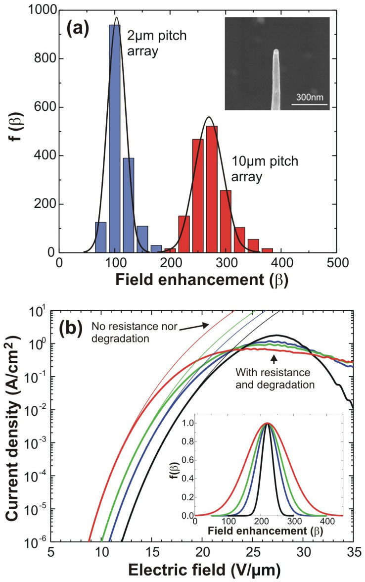
Figure 3(a) shows the measured f(β) for arrays of 2 μm and 10 μm pitch. The inset shows a typical high resolution scanning electron micrograph of a single CN emitter. The typical Gaussian f(β) distributions are narrow and have full-width half maxima of 29 and 61, respectively, and adopt an exp(β2) form. This is in stark contrast to spaghetti-like CN thin film emitters, formed by screen printing, vacuum filtration and other chemi-douche processing, which exhibit a slower decaying exponential tail of the form exp(β) (data not shown). Narrow β distributions offer increased spatial uniformity and enhanced emitter longevity that are temporally stable (ΔI/I of ≤ 10%) at the expense of higher turn-on voltages.
Figure 3.

(a) f(β) histograms and corresponding Gaussian fits, for CN arrays of 2 µm and 10 µm pitch. The field enhancement peak f(β) for the 2 µm CN has a center at βo = 104 and FWHM = 39, and the 10 µm; βo = 271 and FWHM = 61. The inset shows an electron micrograph of an individual CN (Scale bar: 300 nm). (b) Modeled current density as a function of applied electric field and increasingly broad f(β) (inset).
Modelled deviation from Fowler-Nordheim and the emission implications of f(β)
We now model the field emission curves of our CN arrays by adapting conventional FN emission (eq. (1)) by including f(β), emitter degradation, and emitter axial resistance. For a pitch of 10 µm, arrays formed from CNs of height of 5 µm and diameter of 45 nm, our model suggests βemitter = 220, which correlates well for geometric estimates based on a simple ellipsoidal cylinder, (β ≈ h/r = 200). The individual emitter breakdown current was modeled at 5 µA. Figure 3(b) shows the modelled emission I-V curve of four arrays as a function of four increasingly broad f(β), each shown in the inset. The narrowest f(β) (black), which represents a densely packed array experiencing high shielding, offers the highest maximum current due to the greater number of emitters at the expense of an increased higher turn-on field. In comparison, the broadest f(β) (red) facilitates a reduction in turn-on potential of around 35% due to a larger variation in emitter enhancement factor mediated by the sparser array and which is most likely to be deemed as a “high” performing emitter, often at the expense of long term temporal stability as the individual dominating emitters more readily burn-out. We model the typical deviation from conventional FN-type behavior via the inclusion of emitter degradation (burn-out) and axial resistance. As illustrated in Figure 3(b), the inclusion of such non-idealities reveals that broad f(β) distributions tend to reduce the peak emission current substantially (by a factor of more than three) as there are less emitters and individual emitters tend to dominate the emission and subsequently sublime before other emitters are activated.
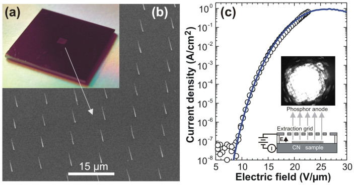
Using our f(β) measurements and the derived model it is possible to predict the global emission performance of any regular array of vertically aligned one-dimensional emitters given suitable knowledge of the geometry (radius, height, pitch) as well the typical electrical characteristics of individual emitters (axial and interfacial resistance, breakdown current). Figures 4(a) and (b) show optical and scanning electron micrographs of a fabricated 10 μm pitch CN array, and Figure 4(c) depicts the measured FE data (ο), the experimental setup and the integrated intensity optical map (inset). The emission curve model was determined a priori to device measurement. Data was fitted (solid line) using the model developed above and detailed in Figure 3(b). The designed β was 220 with the f(β) as shown. Failure and resultant emission degradation was modeled to occur at 3.5 µA/emitter accounting for an equivalent series resistance of 3.5 MΩ. This resistance becomes significant for currents of the order of μA, whilst degradation dominates at high fields, typically > 25 V/μm, where these deviations from near-ideal FN behavior tend to occur in separate regimes to the field enhancement measurements, which we assessed for < 20 V/μm. The model and measurements show exceptional agreement and offer a viable means to the deterministic design, and consequent industrialisation of nano-structured cold cathode electron emitters.
Figure 4.
(a) Optical micrograph of a fabricated 10 μm pitch CN array on a 10 × 10 mm Si substrate and the corresponding (b) scanning electron micrograph (Scale bar: 15 µm). (c) Measured current density as a function of applied electric field and the corresponding modelled emission with the inclusion of axial resistance, emitter degradation and know f(β) (solid line). The inset shows a schematic of the measurement diode setup and depicts the integrated optical intensity map, generated from phosphor coated ITO/glass, showing the spatial distribution in the emission.
Using scanning anode field emission microscopy we have directly evidenced the validity of emitter geometry-based approaches to estimate the field enhancement factor of individual and sparse arrays of periodic, vertically aligned CNs. We also show that such individual emitter field enhancement factors do not represent the field enhancement of an ordered array formed from equivalent emitters and that a strong dependency on emitter pitch was noted. We revealed that narrow distributions in field enhancement factor increase the effective turn-on potential of CN ensembles which are temporally stable, whilst broad distributions manifest as low-turn on emitters, highlighting the potential of CNs in emerging microwave amplifiers, electron microscopy, parallel micro-gun electron lithography systems, and advanced X-ray sources.
Methods
Carbon nanofibre deposition
80 nm dot arrays were defined on degenerately doped Si <001> substrates by casting polymethyl-methacrylate (PMMA) and patterning by electron beam lithography (Nanobeam Inc.). A 10 nm ITO diffusion barrier and 7 nm Ni catalyst were then DC magnetron sputtered and the residual PMMA removed in acetone. Carbon nanofibres were synthetized by plasma-enhanced chemical vapour deposition in a commercially available Aixtron Black Magic system. Carbon nanofibre growth was stimulated by heating the catalyst samples to 700°C (5°C/s) at 5 mbar under 200 sccm NH3: 50 sccm C2H2 for 15 minutes.
Scanning anode field emission microscope
The custom-built scanning anode field emission system consists of a scanning Pt/Ir tip anode with a radius of ~1.5 µm and 90° cone angle attached to a pico-actuator for height (z) displacements (Δz = 50 nm). x-y scanning was achieved using a micro-positioner (Δx,y = 40–400 nm, 5 × 5 mm travel). Samples were grounded and the tip was biased forming a microscopic-resolution anode with applied electric field. The chamber was baked and had a nominal base pressure of < 10−8 mbar.
Author Contributions
M.T.C. wrote the manuscript. K.B.K.T. prepared the figures. M.T.C. and K.B.K.T. analyzed the data, fabricated the samples and conducted the associated metrology. O.G., L.G. and P.L. performed the scanning anode field emission microscopy measurements. O.G. and K.B.K.T. performed the electrostatic and statistical emission simulations. K.B.K.T. and M.T.C. carried out the parallel plate field emission measurements. W.I.M. conceived and supervised the project. All authors contributed to the theoretical analysis.
Acknowledgments
This work was supported by the European Commission through the TECHNOTUBES initiative. M.T.C acknowledges St Edmund's College Cambridge and the generous financial support of the Isaac Newton Trust, Trinity College Cambridge, and the Winston Churchill Memorial Trust.
References
- Baker F. S., Williams J. & Osborn A. R. Field-emission from carbon fibers - new electron source. Nature 239, 96–97 (1972). [Google Scholar]
- De Heer W. A., Châtelain A. & Ugarte D. A carbon nanotube field-emission electron source. Science 270, 1179–1180 (1995). [Google Scholar]
- Wang Q. H. et al. Field emission from nanotube bundle emitters at low fields. Appl Phys Lett 70, 3308–3310 (1997). [Google Scholar]
- Saito Y. et al. Field emission from multi-walled carbon nanotubes and its application to electron tubes. Appl Phys A - Mater 67, 95–100 (1998). [Google Scholar]
- Bonard J. M. et al. Field emission from single-wall carbon nanotube films. Appl Phys Lett 73, 918–920 (1998). [Google Scholar]
- De Jonge N. & Bonard J. M. Carbon nanotube electron sources and applications. Phil T Roy Soc A 362, 2239–2266 (2004). [DOI] [PubMed] [Google Scholar]
- Rosen R. et al. Application of carbon nanotubes as electrodes in gas discharge tubes. Appl Phys Lett 76, 1668–1670 (2000). [Google Scholar]
- Teo K. B. K. et al. Microwave devices - Carbon nanotubes as cold cathodes. Nature 437, 968–968 (2005). [DOI] [PubMed] [Google Scholar]
- Kim H. J. et al. Design and field emission test of carbon nanotube pasted cathodes for traveling-wave tube applications. IEEE T Electron Dev 53 (2006). [Google Scholar]
- Milne W. I. et al. Carbon nanotubes as field emission sources. J Mater Chem 14, 933–943 (2004). [Google Scholar]
- Milne W. I. et al. Carbon nanotubes as electron sources. Phys Stat Sol A 203, 1058–1063 (2006). [Google Scholar]
- Teo K. B. K. et al. Plasma enhanced chemical vapour deposition carbon nanotubes/nanofibres - how uniform do they grow? Nanotech 14, 204–211 (2003). [Google Scholar]
- Teo K. B. K. et al. Uniform patterned growth of carbon nanotubes without surface carbon. Appl Phys Lett 79, 1534–1536 (2001). [Google Scholar]
- Fowler R. H. & Nordheim L. Electron emission in intense electric fields. P R Soc Lond A - ContA 119, 173–181 (1928). [Google Scholar]
- Chen L.-F. et al. Nonlinear characteristics of the Fowler–Nordheim plots of carbon nanotube field emission. Phys Scr 82 (2010). [Google Scholar]
- Semet V. et al. Field electron emission from individual carbon nanotubes of a vertically aligned array. Appl Phys Lett 81, 343–345 (2002). [Google Scholar]
- Xu X. & Brandes G. R. A method for fabricating large-area, patterned, carbon nanotube field emitters. Appl Phys Lett 74, 2549–2551 (1999). [Google Scholar]
- Chen Y. et al. Physical origin of non-linearity in Fowler–Nordheim plots of aligned large area multi-walled nitrogen-containing carbon nanotubes. Mater Sci Eng 327, 16–19 (2002). [Google Scholar]
- Groening O. et al. Field emission properties of carbon nanotubes. J Vac Sci Technol B 18, 665–678 (2000). [Google Scholar]
- Bonard J. M. et al. Tuning the Field Emission Properties of Patterned Carbon Nanotube Films. Adv Mater 13, 184–188 (2001). [Google Scholar]
- Nilsson L. et al. Scanning field emission from patterned carbon nanotube films. Appl Phys Lett 76, 2071–2073 (2000). [Google Scholar]
- Smith R. C. & Silva S. R. P. Maximizing the electron field emission performance of carbon nanotube arrays. Appl Phys Lett 94, - (2009). [Google Scholar]
- Suh J. S., Jeong K. S., Lee J. S. & Han I. Study of the field-screening effect of highly ordered carbon nanotube arrays. Appl Phys Lett 80, 2392–2394 (2002). [Google Scholar]


