Abstract
Vanadium dioxide (VO2) with its unique sharp resistivity change at the metal-insulator transition (MIT) has been extensively considered for the near-future terahertz/infrared devices and energy harvesting systems. Controlling the epitaxial quality and microstructures of vanadium dioxide thin films and understanding the metal-insulator transition behaviors are therefore critical to novel device development. The metal-insulator transition behaviors of the epitaxial vanadium dioxide thin films deposited on Al2O3 (0001) substrates were systematically studied by characterizing the temperature dependency of both Raman spectrum and Fourier transform infrared spectroscopy. Our findings on the correlation between the nucleation dynamics of intermediate monoclinic (M2) phase with microstructures will open a new avenue for the design and integration of advanced heterostructures with controllable multifunctionalities for sensing and imaging system applications.
Vanadium dioxide (VO2) undergoes a metal-insulator transition (MIT) with the resistivity changing sharply in 4–5 orders of magnitude just above the room temperature (341 K). Such unique characteristic can be advantageously utilized in microelectronic devices, terahertz devices, and energy harvesting systems, etc1,2,3,4. The MIT is considered to be accompanied by a structural phase transition from monoclinic to rutile. Recently, the formation of a metastable monoclinic phase of VO2 during the phase transition has attracted much attention, not only from the point of view of the theoretical understanding of the MIT mechanism, but also from the technological consideration in control of the transition properties for device applications. The most stable monoclinic phase of VO2 at room temperature is referred to as the M1 phase, with the β-angle of the unit cell as 122.6°. In this structure, the V atoms are paired and twisted across the octahedral edges5. The localized electron state in this structure is considered to induce the insulating state. However, during the MIT of the insulating M1 phase to the metallic rutile phase, another metastable monoclinic phase with the β-angle of 91.88°, named as the M2 phase, has been reported. This metastable M2 phase is normally induced by either doping or strain. In the M2 structure, half of the V atoms pair but do not twist as in the M1 phase. In contrast, the other half of the vanadium atoms twist, but remain equidistant along the resulting zigzag chain5,6,7,8.
To understand the nature of the M2 phase, both theoretical and experimental efforts have been initiated. It was proposed that the uniaxial stress along [110]R direction would stabilize the M2 phase7. Experimentally, investigations on the M1-M2 transition were mainly focused on single crystalline one-dimensional nanostructures because it is easier to apply a mechanical stress on these structures6,9,10,11,12. There are only a few reports on the observation of the M2 phase in the VO2 thin films, although stress is widely considered as an important feature in thin film systems. Okimura et al. conducted in situ X-ray diffraction (XRD) studies on the epitaxial VO2 films on Al2O3 (0001) grown by pulsed laser deposition, indicating the formation of the M2 phase during the heating process13. More recently, they also found that the M2 phase could be stabilized in polycrystalline thin films at room temperature by using a sputtering technique with inductively coupled plasma14,15. These results have clearly demonstrated that thin film VO2 would be a good model system to study the intermediate phase. However, due to the very complex microstructures of VO2 thin films and related phase transitions, fundamental understanding of the correlations between the microstructures and the occurrence of the M2 phase in VO2 thin films is still lacking. In this paper, we report our effort to systematically study the occurrence of the M2 phase in epitaxial VO2 thin films, using both Raman and Fourier transform infrared (FTIR) spectroscopies at various temperatures. To fully understand the mechanisms of the formation of the M2 phase, the high resolution X-ray diffraction (HRXRD) technique was employed to analyze the strain states and the microstructures.
Results
Briefly, the VO2 thin films were grown on Al2O3 (0001) substrates by using a polymer-assisted deposition (PAD) technique as reported earlier16,17,18. Different thicknesses of VO2 films were synthesized: one set of the sample (labeled as sample Th90) had a thickness of 90 nm and the other set of the sample (labeled as sample Th150) had a thickness of 150 nm. Figs. 1 (a) and (b) show the XRD patterns from θ − 2θ and ϕ scans on the films, respectively. The results indicate that both samples are crystallized in monoclinic VO2 phase (M1) at room temperature and epitaxially grown on the substrates. The epitaxial relationship between the thin film and the substrate was determined to be VO2 (001)||Al2O3 (0001) and VO2 [010]||Al2O3 [ ].
].
Figure 1.
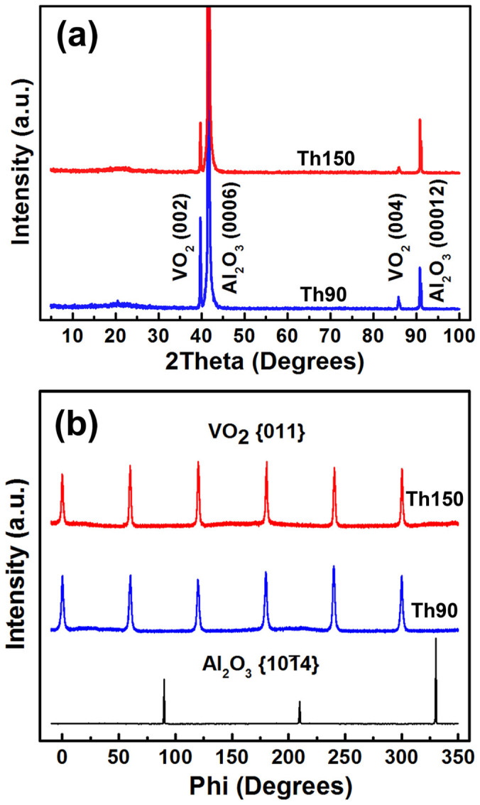
(a) XRD θ − 2θ scans for samples Th90 and Th150, respectively; (b) XRD ϕ scans for samples Th90 and Th150, respectively.
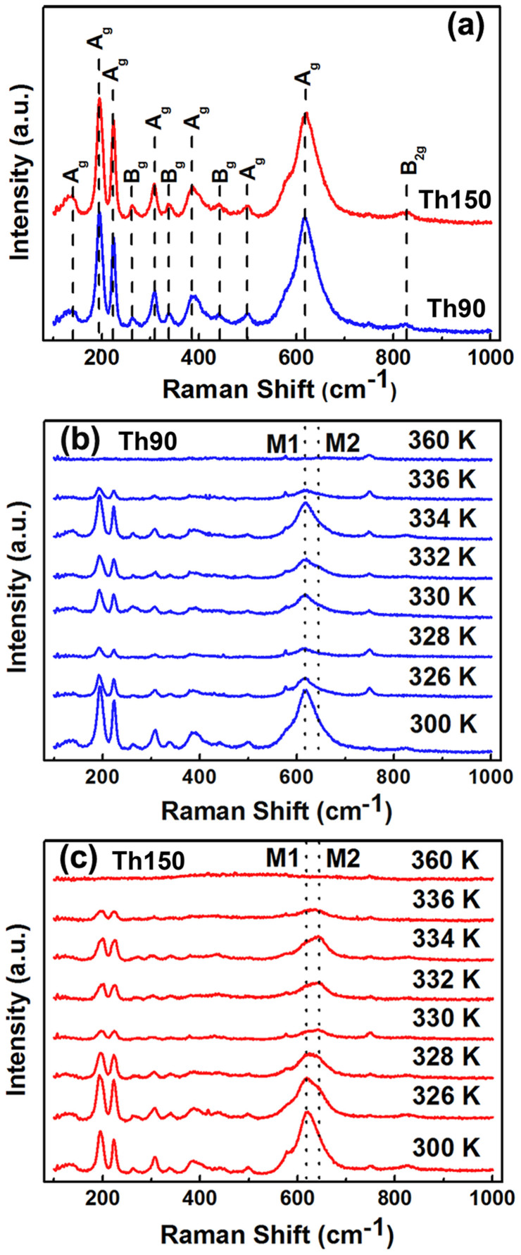
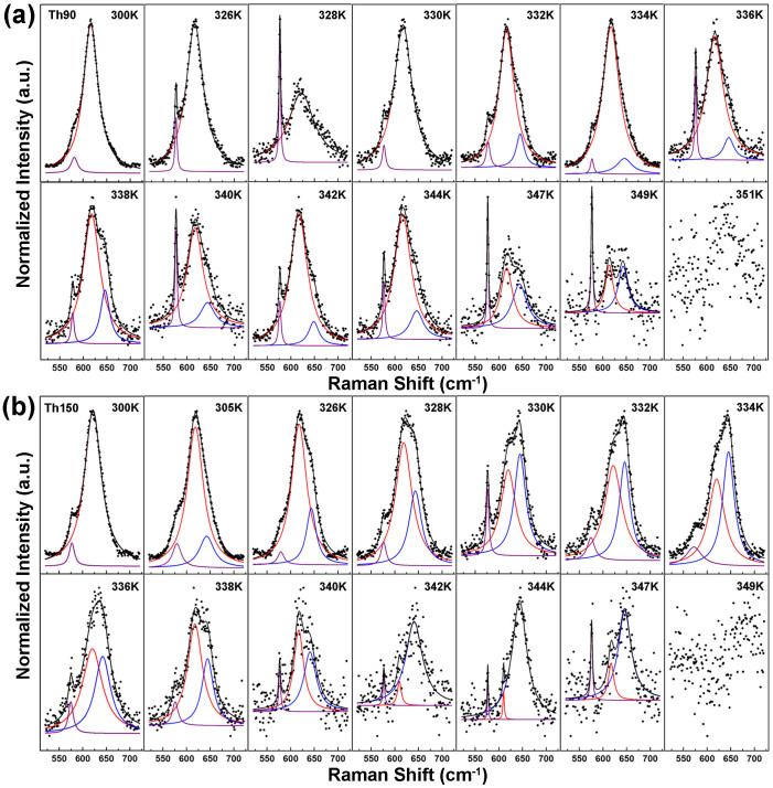
Raman spectroscopy was carried out at various temperatures to check the occurrence of the M2 phase. Samples were heated from 300 to 370 K during the measurement. Each data point was the average from 10 repeated records with the integral time of 10 s. The variation of the temperature was controlled to be less than 0.5 K during the measurement. According to the reported results10,12, the fingerprint for the M1–M2 phase transition is the blueshift of the Raman peak from 618 cm−1 (the M1 phase) to 642 cm−1 (the M2 phase). The blueshift is resulted from the change of Ag vibrate mode in VO2 unit cell. As shown in Fig 2(a), both samples (Th90 and Th150) exhibit almost the same spectra at room temperature. The spectra are identical to those from the pure M1 phase in the bulk single crystalline VO219,20. This result is reasonable considering the good crystalline quality of the as-prepared epitaxial films. With the increase of the temperature, as shown in Figs. 2(b) and (c), the peaks in the Raman spectrum become weaker and finally disappear. This corresponds to the first order transition of crystalline structure from the low symmetry of monoclinic to the high symmetry of rutile. If we look at the detailed Raman spectra during the temperature increase, it is interesting to notice the difference between Th90 and Th150 at around 334 K. Specifically, occurrence of the M2 phase of VO2 with the Raman peak shifting from 618 cm−1 to 642 cm−1 could be clearly observed in sample Th150 instead of sample Th90, as shown in Figs. 2(b) and (c). To verify the results, the Raman spectra between 520 and 720 cm−1 for both samples measured at various temperatures were carefully fit with Lorentz functions. Figs. 3(a) and (b) show the fitting results for Th90 and Th150, respectively. The peaks centered at 577, 618, 642 cm−1 correspond to the characteristic Raman peaks from the Eg mode of sapphire, and the Ag modes of the M1 and M2 phases of VO2, respectively. It is found that both samples are actually composed of mixing phases of M1 and M2 during the MIT. However, the M2 peak started to occur at a much lower temperature for sample Th150 (305 K) than Th90 (332 K). Moreover, the M2 peak is comparable or even higher than the M1 peak for Th150 when the temperature is higher than 330 K. On the contrary, for Th90, the M1 peak is dominant throughout the whole measuring range of temperatures. In other words, both the amount of the M2 phase and the temperature window for the occurrence of the M2 phase are larger in Th150 than Th90 during the MIT.
Figure 2.
(a) Raman spectra for samples Th90 and Th150 at room temperature, respectively; (b) Raman spectra for sample Th90 at temperatures ranging from 300 to 360 K; (c) Raman spectra for sample Th150 at temperatures ranging from 300 to 360 K.
Figure 3.
Lorentz fitting results for the Raman spectra in the range from 520 cm−1 to 720 cm−1 measured at various temperatures for samples Th90 (a) and Th150 (b), respectively. (Black dots are the original data, black lines are the Lorentz fitting line, purple lines indicate the Eg mode of sapphire, red lines indicate the Ag mode of the M1 phase of VO2, and blue lines indicate the Ag mode of the M2 phase of VO2.)
To have a better understanding of the phase transition, IR transmission properties of the samples were measured by using the IR light with different wavelengths at different temperatures. Both the as-prepared samples, Th90 and Th150, exhibit strong modulation of IR transmission at room temperature in the wavelength range from 2500 to 5000 nm, as shown in Fig. 4(a). The transmittance becomes lower as the film thickness increases, possibly due to the stronger absorption from a thicker film. Fig. 4(b) is the IR transmittance measured at various temperatures with a wavelength of 4000 nm. Hysteresis loops were observed from both samples as the results of the intrinsic MIT properties of VO2. The differential curves of the IR transmittance versus temperature are plotted in Fig. 4(c). If we fit these differential curves using Gaussian functions, as shown in the dotted lines in Fig. 4(c), two peaks located at different temperatures (332.1 K and 334.5 K) are observed in sample Th150 during the cooling process, whereas no such obvious split is observed in sample Th90. The two peaks in sample Th150 are most likely to be related to the M1–M2 transition and M2-rutile transition, respectively, which is in good agreement with the M2 occurrence observed in the Raman spectra.
Figure 4.
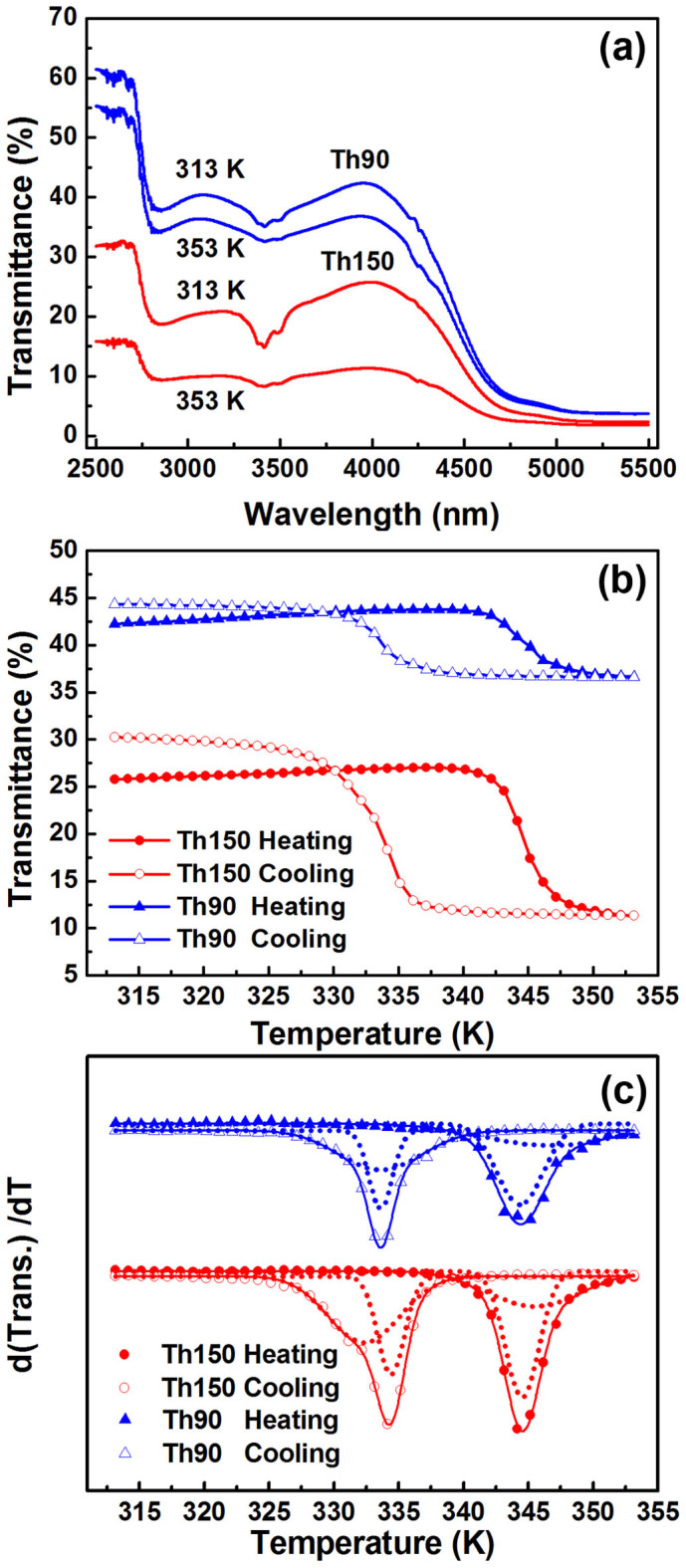
(a) FTIR spectra for samples Th90 and Th150 at 313 K and 353 K, respectively; (b) IR transmittance versus temperature for samples Th90 and Th150, respectively; (c) differential curves of transmittance versus temperature for samples Th90 and Th150, respectively (the dotted lines indicated the fitting results of these differential curves using Gaussian functions).
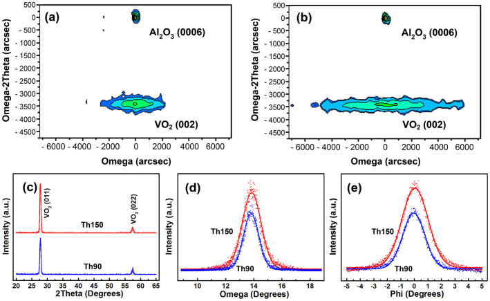
To understand the mechanism of the occurrence of M2 phases, the strain states/distributions of the thin films were characterized by using HRXRD. Similar to the strain distribution analysis for the other epitaxial oxide thin films21,22,23,24,25,26, the strain states can be determined by characterizing the changes in related diffraction peak positions, which reflect the changes in the lattice parameters. The reciprocal space maps (RSMs) were recorded around Al2O3 (0006) and VO2 (002) for samples Th90 and Th150, as shown in Figs. 5(a) and (b), respectively. It is found that the positions of VO2 (002) for both samples are almost the same, i.e., at about 3400 arcseconds lower than the diffraction spots from Al2O3 (0006). The lattice parameters of the c-axis for both samples (Th90 and Th150) are estimated to be 5.3730 Å. Comparing to the lattice parameter of bulk VO2, 5.3820 Å (JCPDS 82-0661), a compressive strain of −0.17% was found along the c-axis for both samples. Under the assumption of constant unit-cell volume, a tensile strain along [011]M1 is expected. By tilting the samples with the setting of χ = 44.8416°, XRD θ − 2θ scanning patterns were collected to measure the in-plane lattice parameters along the [011]M1 direction of the as-prepared VO2 thin films, as shown in Fig. 5(c). The [011]M1 lattice parameters were determined to be 3.208 Å and 3.209 Å for samples Th90 and Th150, respectively. Comparing with its bulk parameter (3.2034 Å), tensile strains of 0.14% and 0.17% for samples Th90 and Th150 were estimated along the [011]M1 direction, respectively.
Figure 5.
(a) RSM around Al2O3 (0006) and VO2 (002) for sample Th90; (b) RSM around Al2O3 (0006) and VO2 (002) for sample Th150; (c) tilted XRD θ − 2θ scans (χ = 44.8416°) for samples Th90 and Th150, respectively; (d) Gaussian fittings of ω rocking curves of VO2 (011) for samples Th90 and Th150, respectively; (e) Gaussian fittings of ϕ scans of VO2 (011) for samples Th90 and Th150, respectively.
Discussion
The [011]M1 would be changed to [110]R when the monoclinic phase M1 is changed to rutile structure27. Therefore, the tensile strains may induce the formation of the M2 phase in both samples, Th90 and Th15011. Nevertheless, the temperature window for the occurrence of the M2 phase can be quite narrow due to the very weak strains. Although the values of the tensile strain in samples Th90 (0.14%) and Th150 (0.17%) are very close to each other, the occurrence window for the M2 phase is very different. More exactly, the amount of M2 phase and the temperature window for the occurrence of the M2 phase are much larger in Th150 than Th90, leading to the clear direct observation of M2 phase in sample Th150 rather than in Th90 under the exactly same experimental set up, as demonstrated by the temperature dependency of Raman spectrum and FTIR spectrum shown above.
To clarify the different occurrence window of the M2 phase in these two epitaxial VO2 thin films, peak spreading of the as-grown films were analyzed by HRXRD ω and ϕ scans. As shown in Figs. 5(a) and (b), the full width at half maximum (FWHM) of ω − 2θ scans around VO2 (002) (along the y-axis in Figs. 5(a) and (b)) are almost the same for samples Th90 and Th150, indicating the similar global strain states of both films. However, the FWHM of the ω scan (along the x-axis in Figs. 5(a) and (b)) for the Th150 sample is much wider than that for the Th90 sample. Similar results (as shown in Fig. 5(d)) were observed in the ω scan rocking curve of VO2 (011) where the sample was tilted by χ = 44.8416°. Theoretically, the FWHM of the ω scan (βm) comes from several sources28:
 |
where β0 is the intrinsic width of X-ray, βd is from optical path of the X-ray equipment, βr depends on the radius of curvature of the sample, βl depends on the grain size of the sample, and βα is the broadened width due to the screw dislocations of the sample. Under the same measurement set-up, equation (1) clearly suggests that the difference in the FWHM of the ω scan should be from the broadened width induced by screw dislocations or grain boundaries, i.e. the value of (βl + βα) in sample Th150 is higher than that in sample Th90. On the other hand, it is known that the density of edge dislocations can be estimated from the peak broadening of the ϕ scan. As shown in Fig. 5(e), the larger FWHM of the ϕ scan peaks for sample Th150 than that for sample Th90 suggests higher density of edge dislocations in the sample Th150. The higher densities of both screw dislocations and edge dislocations may induce higher density of domain/grain boundaries in sample Th150. These domain/grain boundaries may result in a strong impact on the nucleation of the M2 phase11,20,27,29. The low energy at the domain/grain boundaries would promote the nucleation of the new phase. Thus, the richer domain/grain boundaries in sample Th150 would increase the opportunities for the formation of the M2 phase, which either increases the amount of M2 domains or broadens the temperature windows for the occurrence of an M2 phase. This explains the clear direct observation of the M2 phase during the MIT in sample Th150 rather than in sample Th90.
In conclusion, the epitaxial VO2 thin films were prepared on Al2O3 (0001) using a polymer-assisted deposition technique. The intermediate M2 phase was clearly observed in the thicker thin films by temperature dependent Raman and FTIR spectroscopies. Although HRXRD demonstrated that both the as-prepared samples show very similar tensile strains along the [110]R direction, the higher density of dislocations and domain/grain boundaries may account for the easier nucleation of the M2 phase in the thicker film (150 nm thick). These results are helpful to understand and control the occurrence of an M2 phase as well as the resistivity and IR switching properties during MIT, which are critical to the device applications of VO2 thin films.
Methods
The VO2 thin films were grown on Al2O3 (0001) substrates by using a polymer-assisted deposition (PAD) technique. 2.0 g polyethyleneimine (PEI, average Mn ≈ 60000, Mw ≈ 750000), 3.5 g ethylene diamine tetraacetic acid (EDTA) and 1.4 g NH4VO3 were dissolved in 40 mL distilled water to form a homogeneous polymer precursor solution. The solution was then purified in an Amicon filtration (Amicon 8050) unit and concentrated to get a precursor solution containing 12.53 mg V element per mL, as measured by an Inductively Coupled Plasma Optical Emission Spectrometer (ICP-OES). The as-prepared solution was spin-coated on the Al2O3 (0001) substrates. After that, the precursor films were thermally treated at 480°C in the reduced atmosphere of forming gas (H2 2% and N2 98%) for 1 hour. The spin-coating and thermal treatment process was repeated for various times to achieve films with different thicknesses.
The XRD characterization was conducted using a Bede D1 diffractometer with Cu Kα radiation (λ = 1.54060 Å). HRXRD measurements were set by adopting a Si (220) dual channel collimator and monochromator system to provide a highly collimated Cu Kα1 beam with a wavelength spread less than the natural line width of Cu Kα1 and a divergence of 12 arcseconds. The detector acceptance aperture was strictly limited by a precision slit with the width of 50 μm.
Raman spectra were recorded at various temperatures using a Renishaw Micro-Raman Spectroscopy System. The wavelength of the Raman exciting laser used in this measurement was 532 nm.
The infrared ray (IR) transmittance versus temperature was measured by using a Fourier transform infrared spectrometer (FTIR-8400S) equipped with a home-made temperature controlling unit.
Author Contributions
Y.L. and C.L.C. initiated the topic and Y.L. supervised the project. Y.D.J. conducted the thin films fabrication. Y.D.J., Y.D.X. and B.W.T. conducted the XRD and HRXRD measurements. Z.Y. and C.Q.J. did the Raman spectrum measurements. Y.D.J., Y.Z. and M.G. performed the FTIR measurements. Y.L., Y.D.J., C.L.C. and Q.X.J. analyzed the data and co-wrote the manuscript. All authors reviewed the manuscript.
Acknowledgments
This work was supported by the National Basic Research Program of China (973 Program, No.2011CB301705), the National Natural Science Foundation of China (Nos. 11329402 and 51172036). Y. D. Ji acknowledges the support from the Scholarship Award for Excellent Doctoral Student granted by Ministry of Education, P. R. China. The work at Los Alamos was supported, in part, by the U.S. Department of Energy through the Center for Integrated Nanotechnologies, a U.S. Department of Energy, Office of Basic Energy Sciences user facility at Los Alamos National Laboratory. Los Alamos National Laboratory is operated by Los Alamos National Security, LLC, for the National Nuclear Security Administration of the U.S. Department of Energy under contract DE-AC52-06NA25396.
References
- Wu C. Z., Feng F. & Xie Y. Design of vanadium oxide structures with controllable electrical properties for energy applications. Chem. Soc. Rev. 42, 5157–5183 (2013). [DOI] [PubMed] [Google Scholar]
- Yang Z., Ko C. & Ramanathan S. Oxide Electronics Utilizing Ultrafast Metal-Insulator Transitions. Annu. Rev. Mater. Res. 41, 337–367 (2011). [Google Scholar]
- Liu M. K. et al. Terahertz-field-induced insulator-to-metal transition in vanadium dioxide metamaterial. Nature 487, 345–348 (2012). [DOI] [PubMed] [Google Scholar]
- Cao J., Fan W., Zheng H. & Wu J. Thermoelectric Effect across the Metal-insulator Domain Walls in VO2 Microbeams. Nano Lett. 9, 4001–4006 (2009). [DOI] [PubMed] [Google Scholar]
- Marezio M., McWhan D. B., Remeika J. P. & Dernier P. D. Structural Aspects of the Metal-Insulator Transitions in Cr-Doped VO2. Phys. Rev. B 5, 2541–2551 (1972). [Google Scholar]
- Park J. H. et al. Measurement of a solid-state triple point at the metal-insulator transition in VO2. Nature 500, 431–434 (2013). [DOI] [PubMed] [Google Scholar]
- Pouget J. P., Launois H., Dhaenens J. P., Merenda P. & Rice T. M. Electron localization induced by uniaxial stress in pure VO2. Phys. Rev. Lett. 35, 873–875 (1975). [Google Scholar]
- Wu Y. F. et al. Spectroscopic analysis of phase constitution of high quality VO2 thin film prepared by facile sol-gel method. AIP Advances 3, 042132 (2013). [Google Scholar]
- Cao J. et al. Extended Mapping and Exploration of the Vanadium Dioxide Stress-Temperature Phase Diagram. Nano Lett. 10, 2667–2673 (2010). [DOI] [PubMed] [Google Scholar]
- Jones A. C., Berweger S., Wei J., Cobden D. & Raschke M. B. Nano-optical Investigations of the Metal-Insulator Phase Behavior of Individual VO2 Microcrystals. Nano Lett. 10, 1574–1581 (2010). [DOI] [PubMed] [Google Scholar]
- Guo H. et al. Mechanics and Dynamics of the Strain-Induced M1-M2 Structural Phase Transition in Individual VO2 Nanowires. Nano Lett. 11, 3207–3213 (2011). [DOI] [PubMed] [Google Scholar]
- Atkin J. M. et al. Strain and temperature dependence of the insulating phases of VO2 near the metal-insulator transition. Phys. Rev. B 85, 020101 (2012). [Google Scholar]
- Okimura K., Sakai J. & Ramanathan S. In situ x-ray diffraction studies on epitaxial VO2 films grown on c-Al2O3 during thermally induced insulator-metal transition. J. Appl. Phys. 107, 063503 (2010). [Google Scholar]
- Okimura K., Watanabe T. & Sakai J. Stress-induced VO2 films with M2 monoclinic phase stable at room temperature grown by inductively coupled plasma-assisted reactive sputtering. J. Appl. Phys. 111, 073514 (2012). [Google Scholar]
- Watanabe T., Okimura K., Hajiri T., Kimura S. & Sakai J. Phase selective growth and characterization of vanadium dioxide films on silicon substrates. J. Appl. Phys. 113, 163503 (2013). [Google Scholar]
- Jia Q. X. et al. Polymer-assisted deposition of metal-oxide films. Nature Mater. 3, 529–532 (2004). [DOI] [PubMed] [Google Scholar]
- Ji Y. D. et al. Epitaxial growth and metal-insulator transition of vanadium oxide thin films with controllable phases. Appl. Phys. Lett. 101, 071902 (2012). [Google Scholar]
- Ji Y. D. et al. Growth and physical properties of vanadium oxide thin films with controllable phases. MRS Proceedings 1547 (2013). [Google Scholar]
- Wei J., Ji H., Guo W. H., Nevidomskyy A. H. & Natelson D. Hydrogen stabilization of metallic vanadium dioxide in single-crystal nanobeams. Nature Nanotechnol. 7, 357–362 (2012). [Google Scholar]
- Zhang S. X., Chou J. Y. & Lauhon L. J. Direct Correlation of Structural Domain Formation with the Metal Insulator Transition in a VO2 Nanobeam. Nano Lett. 9, 4527–4532 (2009). [DOI] [PubMed] [Google Scholar]
- Gao M. et al. Strain relaxation in epitaxial SrRuO3 thin films on LaAlO3 substrates. Appl. Phys. Lett. 103,141901 (2013). [Google Scholar]
- Lin Y. et al. Strain relaxation in epitaxial (Pb,Sr)TiO3 thin films on NdGaO3 substrates. Appl. Phys. Lett. 96, 102901 (2010). [Google Scholar]
- Lin Y. et al. Epitaxial nature and anisotropic dielectric properties of (Pb,Sr)TiO3 thin films on NdGaO3 substrates. Appl. Phys. Lett. 86, 142902 (2005). [Google Scholar]
- Lin Y. et al. Comparative study of microstructural properties for YBa2Cu3O7 films on single-crystal and Ni-based metal substrates. J. Mater. Res. 20, 2055–2060 (2005). [Google Scholar]
- Lin Y. et al. Anisotropic in-plane strains and dielectric properties in (Pb,Sr)TiO3 thin films on NdGaO3 substrates. Appl. Phys. Lett. 84, 577–579 (2004). [Google Scholar]
- Xiong Y. M. et al. Raman spectra in epitaxial thin films of La1-xCaxMnO3 (x = 0.33,0.5) grown on different substrates. Phys. Rev. B 70, 094407 (2004). [Google Scholar]
- Tselev A. et al. Symmetry Relationship and Strain-Induced Transitions between Insulating M1 and M2 and Metallic R phases of Vanadium Dioxide. Nano Lett. 10, 4409–4416 (2010). [DOI] [PubMed] [Google Scholar]
- Ayers J. E. The measurement of threading dislocation densities in semiconductor crystals by X-ray diffraction. J. Cryst. Growth 135, 71–77 (1994). [Google Scholar]
- Lin Y. & Chen C. L. Interface effects on highly epitaxial ferroelectric thin films. J Mater Sci 44, 5274–5287 (2009). [Google Scholar]


