Abstract
The accumulation of defects, and in particular He bubbles, can have significant implications for the performance of materials exposed to the plasma in magnetic-confinement nuclear fusion reactors. Some of the most promising candidates for deployment into such environments are nanocrystalline materials as the engineering of grain boundary density offers the possibility of tailoring their radiation resistance properties. In order to investigate the microstructural evolution of ultrafine- and nanocrystalline-grained tungsten under conditions similar to those in a reactor, a transmission electron microscopy study with in situ 2 keV He+ ion irradiation at 950°C has been completed. A dynamic and complex evolution in the microstructure was observed including the formation of defect clusters, dislocations and bubbles. Nanocrystalline grains with dimensions less than around 60 nm demonstrated lower bubble density and greater bubble size than larger nanocrystalline (60–100 nm) and ultrafine (100–500 nm) grains. In grains over 100 nm, uniform distributions of bubbles and defects were formed. At higher fluences, large faceted bubbles were observed on the grain boundaries, especially on those of nanocrystalline grains, indicating the important role grain boundaries can play in trapping He and thus in giving rise to the enhanced radiation tolerance of nanocrystalline materials.
The performance of materials in extreme environments poses important fundamental questions about the behaviour of condensed matter under far-from-equilibrium conditions. These conditions create challenges in materials design and synthesis as highlighted in a recent report1. Extensive research has focused on ion irradiation of metals2,3, semiconductors4 and soft materials5 to elucidate the response of these materials to extreme conditions. For example, the conditions found in nuclear fusion reactors have triggered recent research into the radiation tolerance of plasma facing components6, resistance to morphological changes7,8,9 and degradation of their mechanical properties10,11,12. Athough extensive work6,13 has focused on identifying candidate materials such as refractory metals (for example, tungsten and molybdenum), fundamental understanding of the atomistic processes which give rise to their radiation resistance has been limited by the small number of studies14,15,16, in which the dynamic response of these materials is observed directly.
In the context of plasmas in nuclear fusion reactors, tungsten is considered one of the best options as a plasma facing component (PFC) material17,18. However, it is known that irradiation of tungsten with He (one of the main products of nuclear fusion reactions) can lead to microstructural changes such as bubbles19, pores20, nanostructures9 and fuzz formation21 in addition to radiation induced hardening7 and embrittlement13. In the quest for so-called “radiation resistant” materials, efforts have included investigations into novel ultrafine- and nanocrystalline-grained materials22,23 (such as tungsten in the current study) due to the conjecture that radiation resistance can be improved by increasing the grain-boundary area24,25. In the context of the current study, we define a radiation resistant material as one which will demonstrate reduced surface nanostructure formation under plasma facing conditions. Grain boundaries are known to be good He and defect sinks26,27,28, both of which can drive the aforementioned microstructural changes29. Research studies on nanocrystalline grained metals (such as copper30, gold31 and nickel30) and ceramics (such as ZrO2)32 have demonstrated higher radiation resistance with respect to lower defect densities when compared to their commercially available larger-grained forms.
Recent molecular dynamic simulations by Bai et al.33 demonstrated the role of grain boundaries in annihilating interstitial defects and vacancies. In their work interstitials, which are highly mobile15,34,35, were shown to rapidly be absorbed by grain boundaries and subsequently be emitted to combine with vacancies approaching the grain boundary. Furthermore, enhancement of vacancy hopping (i.e. migration) at grain boundaries loaded with interstitials was observed. Grain boundaries can also trap He atoms36 and thus decrease the concentration of He intragranularly. Our hypothesis is that an increased grain-boundary density leads to an increased fluence threshold (or by definition a more “radiation-tolerant” material) in the matrix for bubble growth, bubble coalescence and resulting nanostructured morphology at the surface if their formation depends on the same as proposed in the literature9,37.
To understand the effect of grain-boundary density on the radiation tolerance of tungsten and their role in trapping He, transmission electron microscopy (TEM) investigations are invaluable especially when performed with in situ ion irradiation. The current study presents the first TEM results of in situ low-energy He+ ion irradiation of ultrafine-grained and nanocrystalline-grained tungsten. The coexistence of ultrafine (<500 nm) and nanocrystalline (<100 nm) grains23 adjacent to each other enabled observation of the radiation response of both types of grains compared under exactly the same temperature and irradiation conditions. We define grain size by considering the distance an irradiation-induced defect within a grain would have to migrate in order reach its nearest grain boundary. For example, in a nanocrystalline grain with a nominal characteristic length of 100 nm an irradiation-induced defect is always <50 nm from a grain boundary.
By directly observing the behaviour, size, geometry and distribution of bubbles as the He+ ion fluence was increased, it was possible to explore the role of grain boundaries in mitigating bubble formation in the matrix. Microstructural and morphological changes as observed in the current study can be correlated with enhanced radiation resistance of bulk ultrafine tungsten materials. This is of vital importance to the scientific community working on these materials for extreme irradiating environments. This work also provides important observations that complement recent findings of He accumulation at semi coherent interfaces38. In these studies, large He storage concentrations are attained by the stability of He platelets under irradiation. Although the materials studied were different from our studies, the role semi coherent interfaces have on large He accumulation can be further elucidated by our findings.
Results
In order to gain a better understanding of the fundamental mechanisms which govern the behaviour of defect dynamics in tungsten under reactor conditions, consider the 950°C and 2 keV He+ ion irradiation conditions used in the current study. Vacancy migration (with an activation energy of 1.7 eV)35 in tungsten occurs at temperatures over 800°C whilst rapid interstitial migration (with an activation energy of 0.054 eV)34 occurs at room temperature. Under the irradiation conditions reported here, vacancy migration, bubble migration and bubble coalescence can occur29. The particular novelty of this work is the investigation of grain boundary density engineering to control defects under extreme and far-from-equilibrium conditions. The grain boundary areal density in ultrafine- and nanocrystalline-grained tungsten is far greater than that found in the microstructures of commercially available tungsten which typically has grain sizes that range from 1–10 μm. He ions are trapped in grain boundaries (2D trapping) and dislocation cores (1D trapping) where He ions have limited diffusion compared to in the matrix (3D trapping)27. A large energy barrier for He diffusion back into the matrix makes these grain boundaries act as He sinks and effective barriers for intergranular diffusion of He particles. It is expected that bubbles will nucleate on the boundaries of grains with dimensions approaching the mean free path of migrating He and He-induced defects in preference to nucleating within those grains.
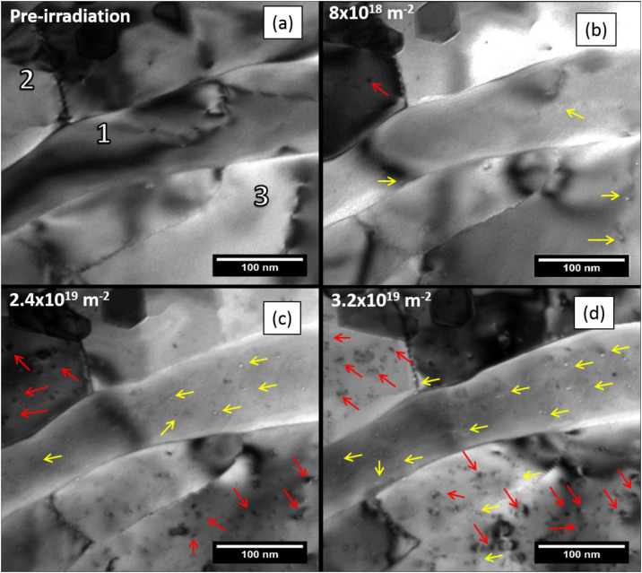
Figures 1(a)–(d) show in situ TEM micrographs of a sample containing both ultrafine- and nanocrystalline-grains. Grain 1 is defined as a nanocrystalline grain with a nominal characteristic length <100 nm and grains 2 and 3 as ultrafine grains with nominal characteristic lengths >100 nm. The evolution of defects induced by low energy He+ ion irradiation shown in Figure 1 occurred under continuous irradiation over a fluence range of 0 to 3.2 × 10¹⁹ ions.m−2. The TEM micrographs shown were all taken in underfocus conditions and so consequently the He bubbles appear with bright contrast on the inside of the bubble and thus small bubbles appear as bright spots. The mean number of atomic displacements generated per incident 2 keV He+ ion was calculated using SRIM to be between 6 and 7 events. The maximum range was calculated to have been about 30 nm and so within this distance there will have been sufficient numbers of vacancies for bubble formation to occur via He trapping by vacancies and vacancy clusters.
Figure 1.
TEM micrographs of in situ 2 keV He+ ion irradiation of tungsten at 950°C showing: (a) nanocrystalline (1) and ultrafine (2 and 3) grains before irradiation; (b) at a fluence of 8 × 10¹⁸ ions.m−2 and after bubble nucleation (bubbles indicated by yellow arrows); (c) after irradiation to a fluence of 2.4 × 10¹⁹ ions.m−2 showing point defect cluster formation (indicated by red arrows) occurred predominantly in grains 2 and 3; and (d) after irradiation to a fluence of 3.2 × 10¹⁹ ions.m−2 with a higher areal density of point defect clusters and small dislocation loops evident in grains 2 and 3 whilst grain 1 demonstrates a uniform distribution of bubbles and a significantly lower areal density of defect clusters and dislocation loops. (arrows guide the eye to aid in identifying respective defects).
Bubbles around 5 nm in size were observed at a fluence of 8 × 10¹⁸ ions.m−2. At 2.4 × 10¹⁹ ions.m−2, defect clusters began to evolve into discernible dislocation loops in the ultrafine grains (see Figure 1(c) grains 2 and 3). However, in the nanocrystalline grains the main change was an increase in the areal density of bubbles with a significantly lower density of defect clusters and dislocations (see Figure 1(c) grain 1). Up to the end fluence of 3.2 × 10¹⁹ ions.m−2, the mean bubble size increased in all grains (see Figure 1(d) grain 1) but was largest in the nanocrystalline grains. In ultrafine grains 2 and 3, large defects clusters and dislocations were also observed (see Figure 1(d)) at the same fluence.
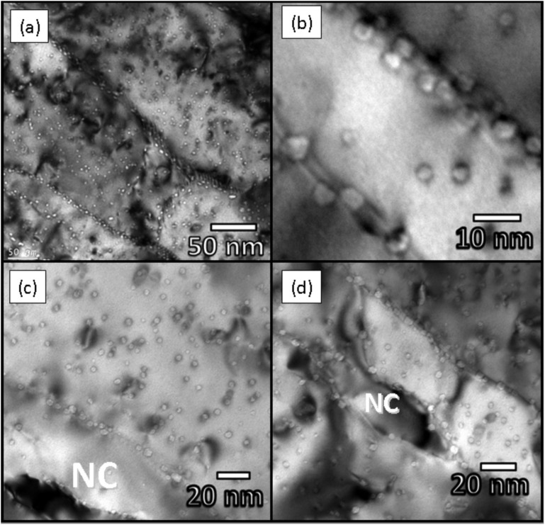
Figure 2(a) shows another selection of grains at a fluence of 3.6 × 10¹⁹ ions.m−2. The largest bubbles were observed on grain boundaries (see Figure 2(b)) and in many cases appeared faceted. This can occur in bubbles when the size becomes sufficiently great such that it becomes energetically favourable to reduce the surface energy of the cavity by diverging from a spherical geometry39. The larger sizes and areal densities of He bubbles on grain boundaries demonstrate how grain size can be used as tools to engineer reduced levels of He bubble formation in the matrix. This will mitigate bubble coalescence in the matrix and/or subsequent intersection with a free surface and thus allow possible control over surface nanostructure formation. However, enhanced grain boundary grooving40 and degradation of mechanical properties (for example, reduced creep resistance)41 are likely to occur due to the production of large bubbles on the grain boundaries. This will be an important consideration in the application of grain size engineering to control the radiation tolerance of tungsten in the context of plasma facing components for magnetic nuclear fusion applications.
Figure 2.
Ultrafine and nanocrystalline grains in tungsten after irradiation with 2 keV He+ to a fluence of 3.6 × 10¹⁹ ions.m−2 at 950°C: (a) overview of typical microstructure of sample; (b) higher magnification micrograph showing grain boundaries decorated with bubbles; and (c)–(d) nanocrystalline grains (denoted NC) demonstrating significantly lower areal densities of bubbles compared to ultrafine grains.
Discussion
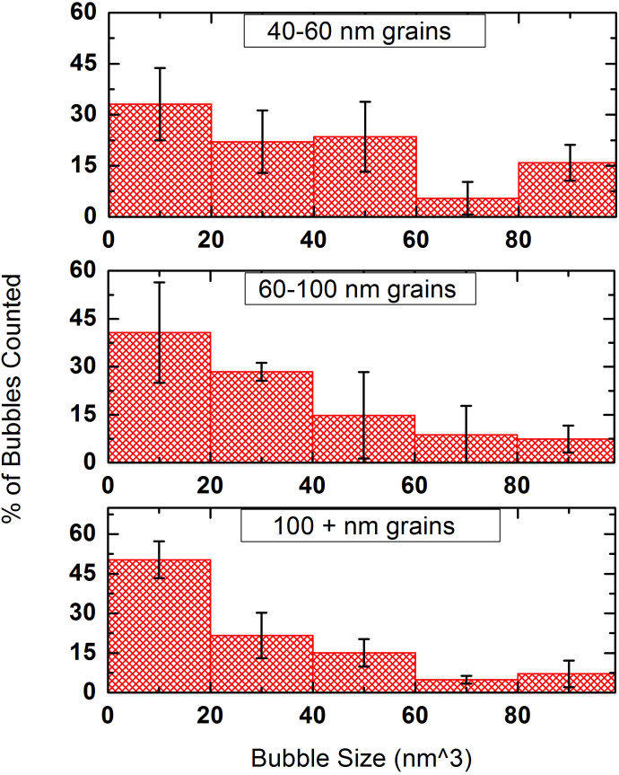
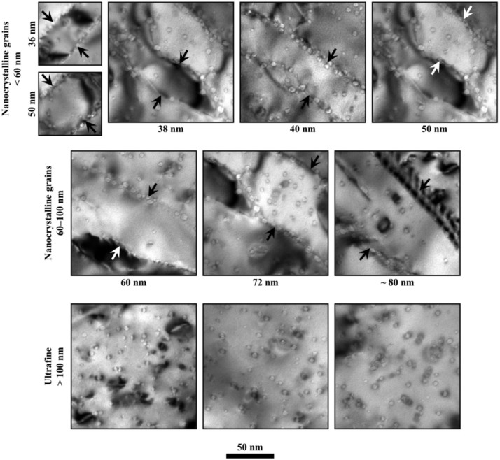
To illustrate the effects of grain size on bubble formation in the matrix, the bubble size distributions for grains of different dimensions are shown in Figure 3. TEM micrographs showing bubble densities in different grain sizes are shown in Figure 4. To perform the bubble size distribution analysis, TEM micrographs were captured from multiple regions and measurements made on the observable bubbles. The grain categories were determined by the grain's smallest dimension across its “width” and not its “length” (note: most grains were an elongated shape). Three grains were analysed for the 40–60 nm range, three grains were analyzed for the 60–100 nm range, and seven grains were analysed for the 100+ nm range. For bubble distribution analysis, the volumes of 446 bubbles (70 (40–60 nm range), 101 (60–100 nm range), and 275 (100+ range) were calculated assuming spherical geometry. These bubbles were randomly selected from the grains in each size category. Since the number of grains for each category available was low, error in bubble counts is given by the square root of the counts. This is a reasonable assumption because our counts are high and based on TEM observations these grains are good representations of their respective grain size category. By sampling all adjacent grains in a region, any bias from preferential selection of grains by the observer were minimized.
Figure 3. Size distributions of bubbles observed in grains of various dimensions at a fluence of 3.2 × 10¹⁹ ions.m−2.
Bubbles located on grain boundaries were not counted, e.g. only intragranular bubbles are counted. The number of bubbles is counted for each grain size category and a standard deviation is calculated based on the number of grains investigated in each grain size category. The small sample size resulted in large error bars in some bubble size categories.
Figure 4. TEM micrographs of different grain sizes showing different bubble densities at a fluence of 3.2 × 10¹⁹ ions.m−2.
Scale marker applies to all micrographs.
The bubble size distributions, which are summarized in Figure 3, revealed a tendency for nanocrystalline grains of less than around 60 nm demonstrated a lower areal density compared to larger nanocrystalline grains (60–100 nm) and ultrafine grains (100–300 nm) (Figure 4). This can be understood by considering the nucleation of bubbles in small grains: as grain boundaries are vacancy sinks they reduce the probability that a migrating He atom will form a He-vacancy complex nucleating a bubble in the matrix; conversely, the probability that the He atom will instead encounter and be absorbed by an existing bubble will be increased. Thus smaller grains will exhibit fewer but larger bubbles. Figure 3 demonstrates that nanocrystalline grains have higher percentage of large bubbles. Furthermore, the grain boundaries of nanocrystalline grains with characteristic lengths of <60 nm were decorated with larger (with respect to the average bubble observed) mostly-faceted bubbles (see Figures 2(b)–(d) and Figure 4) than the ultrafine grains. This predominance of larger faceted bubbles here is further evidence of enhanced migration (compared to commercial grain tungsten) of He atoms and vacancies to the grain boundaries of the nanocrystalline grains.
In addition to bubble nucleation and growth, defect cluster formation and evolution was also observed under ion irradiation. The defect clusters are interstitial in nature as interstitials are in surplus relative to vacancies; the latter having agglomerated together with He atoms to form bubbles. The high binding energy of a large vacancy-He complex renders it stable42 and can also lead to defect clustering through the process of trap mutation43 or loop punching8. Trap mutation is defined as the process in which over-pressurized bubbles emit interstitials in order to increase their volume and loop punching is a similar process in which an interstitial-type dislocation loop is generated.
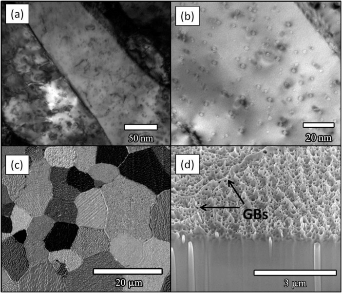
In contrast to nanocrystalline grains, some ultrafine grains showed a high areal density of defects (see Figure 5a). Other ultrafine grains featured homogenous distributions of bubbles with diffraction contrast associated with them and a relatively lower areal density of defects (see Figure 5b). Although over-pressurized bubbles have never been conclusively observed under irradiation conditions, which induce atomic displacements44, we find these bubbles are consistent with loop punching and/or trap mutation mechanisms, which require that the bubbles be over-pressurized.
Figure 5. He+ ion irradiated tungsten samples.
TEM and SEM micrographs of ultrafine-grained tungsten taken at room temperature after being irradiated with 2 keV He+ to a fluence of 3.2 × 10¹⁹ ions.m−2 at 950°C: (a) adjacent ultrafine grains with high concentrations of point defect clusters and dislocations; and (b) an ultrafine tungsten grain with a uniform areal bubble density. The diffraction contrast around the bubbles suggests they are combined with dislocation loops and/or are over pressurized as both these phenomena could induce a strain field. Panel (c) shows a secondary electron image formed using a Ga+ ion beam of an ultrafine-grained sample irradiated with 30 eV He+ ions at 1200°C to a fluence of 1026 ions.m−2 in a complementary experiment; and (d) shows a cross-sectional secondary electron image of the sample in (c) showing nanostructured grains decorated with surface pores and a bowed grain boundary.
The differences observed in the radiation response of various ultrafine grains are likely to be indicative of a dependence on the grain orientation relative to the direction of the ion beam. This can be due to ion beam channelling effects45. In a separate work, we have identified that grains of 001 orientation result in greater surface nanostructure formation than those of 110 or 111 orientation. Figure 5(c) shows a secondary electron image, formed using a Ga+ ion beam, of a sample which has undergone irradiation enhanced recrystallization38,46,47 with 30 eV He+ ions at 1200°C to a fluence of 1026 ions.m−2. The faceted bubbles observed on grain boundaries and in grains (see Figure 2(b)) may be correlated with structures which form preferentially on grains of particular orientations as observed in experiments on bulk material irradiated at high fluence and temperatures (see Figure 5(c)). Figure 5(d) shows that the grain boundaries were bowed (ruptured upward), an observation, which is correlated with the high density of large faceted bubbles observed in the grain boundaries in this study. Further work is underway to investigate grain orientation effects, the correlation between the shape and orientation of bubbles and surface nanostructure development prior to fuzz formation.
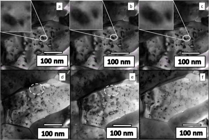
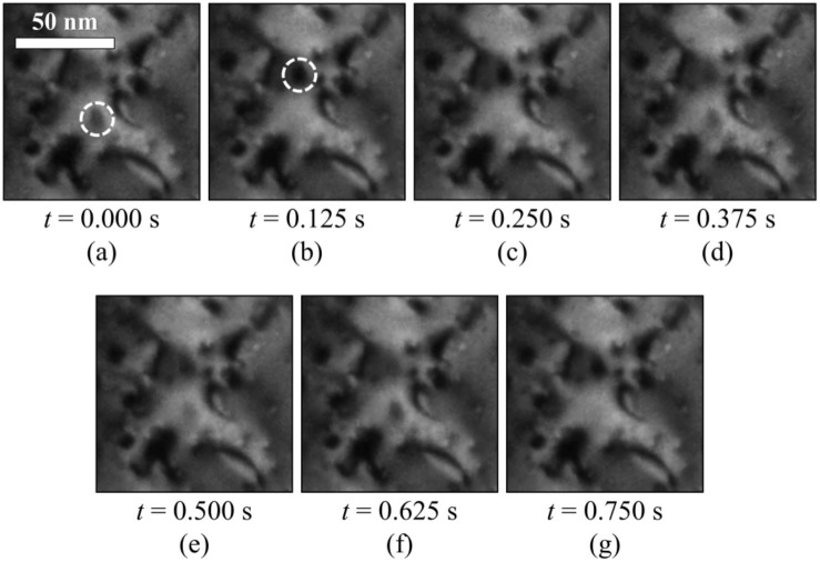
The microstructural evolution of an ultrafine grain including defect formation and development is shown in Figure 6 and corresponds to Grain 2 in Figure 1(a). Defect migration (see Figures 6(a)–(c)), dislocation loop formation, and dislocation pinning (see Figures (d) and (e)) were observed. Another example of dislocation loop shuttling during the irradiation process is shown in Figure 7. Videos S1 and S2 are available online in supplementary material. Interstitial-type defects can be trapped around He-vacancy complexes which can stabilize such high densities of defects14,48,49. The defects continued to evolve for about one minute after ion irradiation was stopped as the system returned to equilibrium (Video S3 is available online in supplementary material). The mobility of defects will have been increased by the irradiation temperature and radiation enhanced diffusion50 effects such as the elevated point defect population.
Figure 6.
Dynamic behavior of defects in an ultrafine grain of tungsten under continuous 2 keV He+ ion irradiation at 950°C (Video S1 available online in supplementary material): (a), (b) and (c) dislocation loop shuttling between two pinning defects (circled by solid white line) from a fluence of 2.8 × 10¹⁹ to 3.2 × 10¹⁹ ions.m−2 (further example is shown in Figure 7); (d) and (e) dislocation migration and coalescence (circled by dashed white line) during irradiation from 3.2 × 10¹⁹ to 3.6 × 10¹⁹ ions.m−2; and (f) a uniform distribution of dislocations with some decorated by bubbles at the end fluence of 3.6 × 10¹⁹ ions.m−2.
Figure 7.
Series of consecutive video frames captured at a fluence of 2.8 × 10¹⁹ ions.m−2 showing a dislocation loop shuttling between two sites indicated by the white dashed circles in (a) and (b). The loop appears to occupy both sites in frames (d) to (f) as the shuttling frequency was greater than the video frame capture rate of 8 Hz. Scale marker in (a) applies to all seven panels. Video S2 is available online in supplementary material.
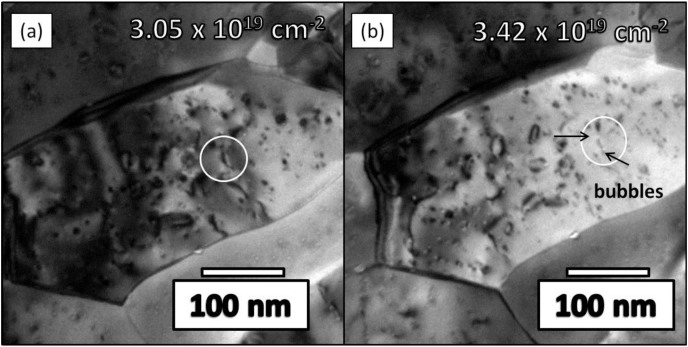
Such a high density of defects and their mobility, which were neglected in the nanostructure formation mechanism suggested by Kajita et al.9,37 may play a role in the changes that occur in tungsten in extreme irradiating environments either directly or through their effects on bubble nucleation, evolution and behaviour. In a recent study by Ohno et al.51, it was demonstrated that the effect of crystallographic orientation on the formation of wavy structures (ripple-shape structures as shown in Figure 5(c)) in tungsten exposed to extreme irradiating environments is related to over-pressurized bubbles pushing the tungsten lattice along its slip planes. Slip can be enhanced by high point defect concentrations and the resulting irradiation enhanced diffusion50 which are both present under the experimental conditions reported in the current study. Therefore, the mechanisms described by Ohno et al. would be further enhanced by these effects. Dislocations are also trapping sites for He particles (1D trapping)36. In the current study, at the end fluence of 3.6 × 10¹⁹ ions.m−2 a homogenous distribution of dislocations, on which bubbles were nucleated (see Figure 8), was observed in the ultrafine grain shown in Figure 6(f). Therefore, dislocations and dislocation loops can act as bubble nucleation sites and can thus affect nanostructure formation on irradiated materials.
Figure 8.
Decoration of dislocations by He bubbles: (a) dislocation (indicated by white circle) formed during 2 keV He+ irradiation of ultrafine tungsten at 950°C at a fluence of 3.1 × 10¹⁹ ions.m−2; and (b) bubbles (indicated with black arrows) observable on the dislocation at the slightly higher fluence of 3.4 × 10¹⁹ ions.m−2.
In summary, the application of TEM with in situ ion irradiation to the study of ultrafine- and nanocrystalline-grained tungsten has revealed several important aspects of the response of this material to low energy He+ ion irradiation at high temperatures. The high radiation resistance of the nanocrystalline grains demonstrated by their resistance to bubble and defect formation in the matrix gives insight into the atomistic mechanisms, which drive these processes. This behaviour is correlated with the previously-reported higher resistance of these materials to fuzz formation which is believed to be initiated by bubble nucleation and coalescence.
The larger ultrafine grains demonstrated a markedly different behaviour compared to nanocrystalline grains indicating the important role of grain boundaries to the response of polycrystalline tungsten to irradiation. Nanocrystalline grains demonstrated lower areal densities of larger bubbles compared to ultrafine grains which featured higher areal densities of bubbles, defect clusters and dislocations. Bubbles were observed to nucleate on these dislocations meaning they can act as the basis of surface nanostructure formation thus demonstrating the importance of defect cluster and dislocation production on the morphology changes which can occur in He+ irradiated tungsten.
The largest bubbles were observed to form on the grain boundaries, rather than in the grains themselves, further highlighting the importance of these features as He sinks. Whilst the accumulation of He in grain boundaries may have significant benefits in terms of the reduction of surface nanostructure formation, it is important to note that this can also lead to degradation in the mechanical properties of tungsten. The engineering of the radiation resistance of tungsten via the control of grain size must take both these phenomena into account. Future work will focus on higher fluence irradiations to examine bubble coalescence, the fundamental process behind nanostructure formation and the effect of grain orientation.
Methods
Tungsten with ultrafine and nanocrystalline grains was produced using an orthogonal machining process which is detailed elsewhere23. For TEM sample preparation, small sections of material were mechanically polished on both sides to obtain 100 μm thick samples. Final thinning was performed by electropolishing with 0.1 wt-% NaOH solution. No variation in mass-thickness contrast, other than that expected of a slightly-wedged sample, was observed in the TEM across the grains suggesting that any preferential etching due to crystallographic orientation and/or grain size was negligible. This is an important consideration when comparing areal densities of features and phenomena, which may be affected by the proximity of free surfaces.
Samples were He+ ion irradiated in situ at 950°C within the JEOL JEM-2000FX TEM at the Microscope and Ion Accelerator for Materials Investigations (MIAMI) facility at the University of Huddersfield which is described in detail elsewhere52. The ion beam energy was 2 keV and was operated with a flux of 3.3 × 10¹⁶ ions.m−2.s−1. In the MIAMI facility, the angle between the sample surface at zero tilt and the ion beam is 60° giving a projected range for 2 keV He+ in tungsten of 10.6 nm as calculated by the Stopping Range of Ions in Matter (SRIM)53 Monte Carlo computer code version 2013. This projected range was within the nominal characteristic length of the ultrafine-and nanocrystalline-grains in the tungsten samples irradiated. The electron energy was 200 keV and the electron beam remained incident normal to the sample surface during ion irradiation so that the evolution of the microstructure could be observed as it occurred and to allow video of the dynamic effects to be captured. The area monitored during the ion irradiation experiment was compared to adjacent regions, which were not under the electron beam (but were ion irradiated) to confirm there were no significant electron-beam induced effects. The sample was mounted and heated in a Gatan Model 652 heating holder with images and video were captured using a Gatan ORIUS SC200 digital camera. Imaging was performed in bright-field TEM conditions and images were taken with ±1.5 μm of defocus. Video was captured at a frame size of 480 × 480 pixels and a frame rate of 8 Hz. Additional post-irradiation analyses at room temperature were performed using a JEOL JEM-3010 TEM and an FEI-TECNAI-20 TEM with electron beam energies of 300 keV and 200 keV respectively.
Author Contributions
O.E. planned the work, performed the post-irradiation characterizations, helped in data analyses and interpretation and wrote the original draft of the paper. J.H. and G.G. performed the in-situ TEM experiment, helped in data analyses, interpretation, and writing the paper. S.G. helped in analyzing the data and writing the paper. T.Q. worked on TEM sample preparation. M.E. prepared the ultrafine and nanocrystalline grained tungsten samples. J.P. Allain worked on data analyses and interpretation, and helped in writing the paper. All co-authors helped in writing the final draft.
Supplementary Material
supplementary video S1
supplementary video S2
Supplementary video S3
Acknowledgments
This research is supported by the U.S. Department of Energy under contract DE-SC0004032. Experimental work using the MIAMI facility was supported by the UK's Engineering and Physical Research Council under grant number EP/H018921/1.
References
- Hemminger J., Fleming G. & Ratner M. Directing Matter and Energy: Five Challenges for Science and the Imagination, http://www.osti.gov/scitech/servlets/purl/935427, (2007) Date of access: 09/03/2014.
- Hung L. S., Nastasi M., Gyulai J. & Mayer J. W. Ion-induced amorphous and crystalline phase formation in Al/Ni, Al/Pd, and Al/Pt thin films. Appl. Phys. Lett. 42, 672–674 (1983). [Google Scholar]
- Wang Z. G., Dufour C., Paumier E. & Toulemonde M. The Se sensitivity of metals under swift-heavy-ion irradiation: a transient thermal process. J. Phys.: Condens. Matter 6, 6733 (1994). [DOI] [PubMed] [Google Scholar]
- El-Atwani O. et al. Real time x-ray studies during nanostructure formation on silicon via low energy ion beam irradiation using ultrathin iron films. Appl. Phys. Lett. 101, 263104 (2012). [Google Scholar]
- Compagnini G., Giannazzo F., Sonde S., Raineri V. & Rimini E. Ion irradiation and defect formation in single layer graphene. Carbon 47, 3201–3207 (2009). [Google Scholar]
- Neu R. et al. Tungsten: an option for divertor and main chamber plasma facing components in future fusion devices. Nucl. Fusion 45, 209–218 (2005). [Google Scholar]
- Yoshida N., Iwakiri H., Tokunaga K. & Baba T. Impact of low energy helium irradiation on plasma facing metals. J. Nucl. Mater. 337, 946–950 (2005). [Google Scholar]
- Minyou Y. Effects of low energy and high flux helium/hydrogen plasma irradiation on tungsten as plasma facing material. Plasma Sci. Technol 7, 2828 (2005). [Google Scholar]
- Kajita S., Sakaguchi W., Ohno N., Yoshida N. & Saeki T. Formation process of tungsten nanostructure by the exposure to helium plasma under fusion relevant plasma conditions. Nucl. Fusion 49, 095005 (2009). [Google Scholar]
- Barabash V., Federici G., Rödig M., Snead L. L. & Wu C. H. Neutron irradiation effects on plasma facing materials. J. Nucl. Mater. 283, 138–146 (2000). [Google Scholar]
- Burchell T. D. A microstructurally based fracture model for polygranular graphites. Carbon 34, 297–316 (1996). [Google Scholar]
- Beck C. E., Roberts S. G., Edmondson P. D. & Armstrong D. E. J. Effect of alloy composition & helium ion-irradiation on the mechanical properties of tungsten, tungsten-tantalum & tungsten-rhenium for fusion power applications. MRS Proceedings 1514, 99–104 (2013). [Google Scholar]
- Federici G. et al. Plasma-material interactions in current tokamaks and their implications for next step fusion reactors. Nucl. Fusion 41, 1967 (2001). [Google Scholar]
- Iwakiri H., Yasunaga K., Morishita K. & Yoshida N. Microstructure evolution in tungsten during low-energy helium ion irradiation. J. Nucl. Mater. 283, 1134–1138 (2000). [Google Scholar]
- Watanabe Y., Iwakiri H., Yoshida N., Morishita K. & Kohyama A. Formation of interstitial loops in tungsten under helium ion irradiation: Rate theory modeling and experiment. Nucl. Instrum. Methods Phys. Res., Sect. B 255, 32–36 (2007). [Google Scholar]
- Evans J. H., Van Veen A. & Caspers L. M. In-situ TEM observations of loop punching from helium platelet cavities in molybdenum. Scr. Metall. 17, 549–553 (1983). [Google Scholar]
- Davis J. W., Barabash V. R., Makhankov A., Plöchl L. & Slattery K. T. Assessment of tungsten for use in the ITER plasma facing components. J. Nucl. Mater. 258, 308–312 (1998). [Google Scholar]
- Lipschultz B. et al. Plasma–surface interaction, scrape-off layer and divertor physics: implications for ITER. Nucl. Fusion 47, 1189 (2007). [Google Scholar]
- Nishijima D., Ye M. Y., Ohno N. & Takamura S. Formation mechanism of bubbles and holes on tungsten surface with low-energy and high-flux helium plasma irradiation in NAGDIS-II. J. Nucl. Mater. 329, 1029–1033 (2004). [Google Scholar]
- Cipiti B. B. & Kulcinski G. L. Helium and deuterium implantation in tungsten at elevated temperatures. J. Nucl. Mater. 347, 298–306 (2005). [Google Scholar]
- Baldwin M. J. & Doerner R. P. Formation of helium induced nanostructure ‘fuzz’ on various tungsten grades. J. Nucl. Mater. 404, 165–173 (2010). [Google Scholar]
- Wei Q. et al. Mechanical behavior and dynamic failure of high-strength ultrafine grained tungsten under uniaxial compression. Acta Mater. 54, 77–87 (2006). [Google Scholar]
- Efe M., El-Atwani O., Guo Y. & Klenosky D. R. Microstructure refinement of tungsten by surface deformation for irradiation damage resistance. Scripta Mater. 70, 31–34 (2014). [Google Scholar]
- Shen T. D. Radiation tolerance in a nanostructure: Is smaller better? Nucl. Instrum. Methods Phys. Res., Sect. B 266, 921–925 (2008). [Google Scholar]
- Shen T. D. et al. Enhanced radiation tolerance in nanocrystalline MgGa2O4. Appl. Phys. Lett. 90, 263115 (2007). [Google Scholar]
- Demkowicz M. J., Hoagland R. G. & Hirth J. P. Interface structure and radiation damage resistance in Cu-Nb multilayer nanocomposites. Phys. Rev. Lett. 100, 136102 (2008). [DOI] [PubMed] [Google Scholar]
- Singh B. N. & Foreman A. J. E. Calculated grain size-dependent vacancy supersaturation and its effect on void formation. Philos. Mag. 29, 847–858 (1974). [Google Scholar]
- Samaras M., Derlet P. M., Van Swygenhoven H. & Victoria M. Radiation damage near grain boundaries. Philos. Mag. 83, 3599–3607 (2003). [Google Scholar]
- Sharafat S., Takahashi A., Hu Q. & Ghoniem N. M. A description of bubble growth and gas release of helium implanted tungsten. J. Nucl. Mater. 386, 900–903 (2009). [Google Scholar]
- Nita N., Schaeublin R. & Victoria M. Impact of irradiation on the microstructure of nanocrystalline materials. J. Nucl. Mater. 329, 953–957 (2004). [Google Scholar]
- Chimi Y. et al. Accumulation and recovery of defects in ion-irradiated nanocrystalline gold. J. Nucl. Mater. 297, 355–357 (2001). [Google Scholar]
- Rose M., Balogh A. G. & Hahn H. Instability of irradiation induced defects in nanostructured materials. Nucl. Instrum. Methods Phys. Res., Sect. B 127, 119–122 (1997). [Google Scholar]
- Bai X.-M., Voter A. F., Hoagland R. G., Nastasi M. & Uberuaga B. P. Efficient annealing of radiation damage near grain boundaries via interstitial emission. Science 327, 1631–1634 (2010). [DOI] [PubMed] [Google Scholar]
- Dausinger F. & Schultz H. Long-range migration of self-interstitial atoms in tungsten. Phys. Rev. Lett. 35, 1773 (1975). [Google Scholar]
- Balluffi R. W. Vacancy defect mobilities and binding energies obtained from annealing studies. J. Nucl. Mater. 69, 240–263 (1978). [Google Scholar]
- Singh B. N., Leffers T., Green W. V. & Victoria M. Nucleation of helium bubbles on dislocations, dislocation networks and dislocations in grain boundaries during 600 MeV proton irradiation of aluminium. J. Nucl. Mater. 125, 287–297 (1984). [Google Scholar]
- Kajita S., Yoshida N., Yoshihara R., Ohno N. & Yamagiwa M. TEM observation of the growth process of helium nanobubbles on tungsten: Nanostructure formation mechanism. J. Nucl. Mater. 418, 152–158 (2011). [Google Scholar]
- Kashinath A., Misra A. & Demkowicz M. J. Stable storage of helium in nanoscale platelets at semicoherent interfaces. Phys. Rev. Lett. 110, 086101 (2013). [DOI] [PubMed] [Google Scholar]
- Niwase K., Ezawa T., Fujita F., Kusanagi H. & Takaku H. Morphology of micro-cavities in nickel during helium bombardment and post-irradiation annealing. Radiat. Eff. 106, 65–76 (1988). [Google Scholar]
- El-Atwani O., Efe M., Heim B. & Allain J. P. Surface damage in ultrafine and multimodal grained tungsten materials induced by low energy helium irradiation. J. Nucl. Mater. (2012). [Google Scholar]
- Scott P. A review of irradiation assisted stress corrosion cracking. J. Nucl. Mater. 211, 101–122 (1994). [Google Scholar]
- Kornelsen E. V. & Van Gorkum A. A. A study of bubble nucleation in tungsten using thermal desorption spectrometry: Clusters of 2 to 100 helium atoms. J. Nucl. Mater. 92, 79–88 (1980). [Google Scholar]
- Caspers L. M., Fastenau R. H. J., Van Veen A. & Van Heugten W. F. W. M. Mutation of vacancies to divacancies by helium trapping in molybdenum effect on the onset of percolation. Phys. Status Solidi A 46, 541–546 (1978). [Google Scholar]
- Evans J. H., Van Veen A. & Caspers L. M. The application of TEM to the study of helium cluster nucleation and growth in molybdenum at 300 K. Radiat. Eff. 78, 105–120 (1983). [Google Scholar]
- Kempshall B. W. et al. Ion channeling effects on the focused ion beam milling of Cu. J. Vac. Sci. Technol., B 19, 749–754 (2001). [Google Scholar]
- Zinkle S. J., Kulcinski G. L. & Mansur L. K. Radiation-enhanced recrystallization in copper alloys. J. Nucl. Mater. 141, 188–192 (1986). [Google Scholar]
- Vaidya W. V. & Ehrlich K. Radiation-induced recrystallization, its cause and consequences in heavy-ion irradiated 20% cold-drawn steels of type 1.4970. J. Nucl. Mater. 113, 149–162 (1983). [Google Scholar]
- Niwase K., Ezawa T., Tanabe T., Kiritani M. & Fujita F. E. Dislocation loops and their depth profiles in He+ and D+ ion irradiated nickel. J. Nucl. Mater. 203, 56–66 (1993). [Google Scholar]
- Odette G. R., Maziasz P. J. & Spitznagel J. A. Fission-fusion correlations for swelling and microstructure in stainless steels: Effect of the helium to displacement per atom ratio. J. Nucl. Mater. 104, 1289–1303 (1981). [Google Scholar]
- Delafond J., Jaouen C., Rivière J. P. & Fayoux C. Ion-beam-induced crystallization of Ni50Al50 amorphous films. Mater. Sci. Eng. 69, 117–121 (1985). [Google Scholar]
- Ohno N. et al. Influence of crystal orientation on damages of tungsten exposed to helium plasma. J. Nucl. Mater. 438, 879–882 (2013). [Google Scholar]
- Hinks J. A., Van Den Berg J. A. & Donnelly S. E. MIAMI: Microscope and ion accelerator for materials investigations. J. Vac. Sci. Technol., A 29, 021003 (2011). [Google Scholar]
- Ziegler J. F., Ziegler M. D. & Biersack J. P. SRIM – The stopping and range of ions in matter (2010). Nucl. Instrum. Methods Phys. Res., Sect. B 268, 1818–1823 (2010). [Google Scholar]
Associated Data
This section collects any data citations, data availability statements, or supplementary materials included in this article.
Supplementary Materials
supplementary video S1
supplementary video S2
Supplementary video S3


