Abstract
While nanowires and nanospheres have been utilized in the design of a diverse array of nanoscale devices, recent schemes frequently require nanoscale architectures of higher complexity. However, conventional techniques are largely unsatisfactory for the production of more intricate nanoscale shapes and patterns, and even successful fabrication methods are incompatible with large-scale production efforts. Novel top-down, iterative size reduction (ISR)-mediated approaches have recently been shown to be promising for the production of high-throughput cylindrical and spherical nanostructures, though more complex architectures have yet to be created using this process. Here we report the presence of a hitherto-undescribed transitory region between nanowire and nanosphere transformation, where a diverse array of complex quasi one-dimensional nanostructures is produced by Rayleigh-Plateau instability-mediated deformation during the progress of a combined ISR/thermal instability technique. Temperature-based tailoring of architecturally diverse, indefinitely long, globally parallel, complex nanostructure arrays with high uniformity and low size variation facilitates the development of in-fiber or free-standing nanodevices with significant advantages over on-chip devices.
Advances in nanoscale fabrication and characterization methods1,2,3,4,5 have led to fundamental changes in the scientific understanding of many fields, and many prototype designs6,7,8 have been well-established using these nanotechnology toolkits. However, the current generation of nanoscale materials, such as nanowires and nanospheres, are not complex enough to serve as building blocks for the design of well-ordered and multifunctional systems analogous to these found in nature9. It is therefore necessary to devise engineering techniques10,11 by which one can exercise a greater level of control over material properties, shapes, morphologies and assembly mechanisms that may facilitate the design of various devices with novel optical, mechanical, thermal and electrical properties12,13,14,15,16.
While there is much interest in the synthesis of architecturally complex and diverse nanoconfigurations, current fabrication methods are incapable of producing such nanoscale elements with efficiencies similar to the large-scale, low-cost, high precision synthesis mechanisms characteristic of biological materials. Bottom-up approaches17,18,19,20,21 are exclusively applicable to the low-throughput production of deep-nanosize structures, and suffer from large variations in product sizes, misalignment issues and the agglomeration of produced nanostructures. Meanwhile, top-down approaches22,23 are generally unsatisfactory for the fabrication of complex nanostructures, and are instead utilized mostly for the production of larger particles. In addition, structures obtained by many of these techniques24,25,26 are scattered on the target substrate and cannot be manipulated individually or as arrays, necessitating a series of post-fabrication alignment processes that may greatly increase production costs. Lithographic methods are likewise not cheap and rapid enough to be applicable for large-scale fabrication efforts.
We had previously described a top-down nanofabrication method27, Iterative Size Reduction (ISR), where step-by-step reduction is utilized to decrease structure dimensions from macro- to nanosizes and produce 1D nanostructure arrays highly suitable for use in various applications28,29. Although ISR is conventionally limited to the production of nanowires, this constraint has recently been overcome by utilizing Rayleigh-Plateau instabilities30,31 to thermally degrade ISR-produced nanowire arrays32. However, while the fabrication of spherical structures was demonstrated using ISR and thermal degradation, more complex architectures have yet to be created using this combination.
Here we report the presence of a transitory region where a diverse array of high-throughput, complex, quasi-1D nanostructures is produced from glass-polymer core-shell nanowires during the progress of a rapid, easy to perform, cost-effective combined ISR-thermal instability technique. Indefinitely long, globally-oriented, in-fibre arrays of nanosprings, shell-embedded nanorods, shell-embedded nanospheres (nanopeapods) and nanochains can be fabricated in succession by halting the thermal degradation process prior to core-shell nanosphere formation. Conceptual underpinnings behind the fabrication of these structures are remarkable and especially nanohelices, represent the first model of nanostructure formation where the resultant structures obey a non-axisymmetric instability condition.
Fabrication of in-fiber nanostructures
A combination of ISR and thermal-manipulation processes is used for the production of nanostructure arrays from a multi-material macroscopic preform. In ISR, amorphous preforms are conventionally drawn in a material-specific temperature region in which viscous forces are balanced with an applied mechanical stress, which facilitates uniform size reduction and can be applied repeatedly until nanoscale structures are produced (Figure 1). We had previously described a multi-step iterative thermal fiber drawing process for 1D nanostructure production, and use it here for the fabrication of core-shell As2Se3-PVDF nanowires. Briefly, a macroscopic preform is produced by successively wrapping PVDF and PES films around an As2Se3 core and drawing the composite structure in multiple elongation steps until nanowires of desired sizes are obtained. Composite fibers with an outer diameter of 400 µm are acquired after the first drawing step, embedded in a PES sheath in self-organized hexagonal arrays of 360 microfibers and redrawn to produce indefinitely long nanowire arrays (see Methods for details). Macroscopic preforms are typically reduced 50-fold in step I, and up to 1000-fold in step II (Figure S1).
Figure 1. Fabrication of novel nanoschemes.
Low temperature, multimaterial fiber drawing method used for the iterative size reduction of a macroscopic layered rod down to core-shell nanowires. Microstructures obtained after the first thermal drawing step are cut in 10 cm strips, arranged in hexagonal arrays of 360 microwires and embedded in dielectric polyethersulfone (PES) prior to a second drawing step. Kilometer-long, ordered As2Se3/PVDF core-shell nanowires are obtained after the second step and can be fabricated in a broad nanowire diameter range (50 nm-1 µm). Structural changes in a nanowire array subjected to heat treatment. Thermal compatibility of chalcogenide glass, PES and PVDF polymers permit the production of different combinations of nanostructures. Gradual increases in temperature result in structural alterations in the nanowire, up to and including the fragmentation of the core region. The structural transition can be halted at any point to obtain the desired nanomaterial configuration.
Heat treatment can then be utilized to induce structural transitions in core-shell nanowires, mediated by the mutually compatible viscoelastic properties of the As2Se3 glass core, PVDF polymer shell and PES matrix sheath, leading to the emergence of a series of nanostructures such as, nanosprings, shell-embedded nanorods, nanopeapods, nanochains until heat-induced fractionation results in the production of core-shell nanospheres (Figure 1). Controlled synthesis of each scheme is achieved by altering the nanowire diameter (d), process temperature (T) and/or process duration (t) within the transitory range, which typically occurs in the 200–280°C region for t = 2 min and d = 90 nm and is increased for lower exposure times (e.g. 220–300°C for t = 10 sec and d = 90 nm) and higher nanowire diameters (e.g. 220–300°C, t = 2 min and d = 200 nm). The fabrication method is scalable across a wide size range and can be used for the production of nano- and microscale structures by altering initial structure profile and dimensions. Amorphous materials, including many chalcogenide glasses, are advantageous for the utilization in these methods due to their continuous glass transition temperatures. Further, since the fractionation behavior is initiated by viscosity and surface tension differences between inner and outer nanowire layers, a core-shell geometry is necessary for the production of the aforementioned nanostructures.
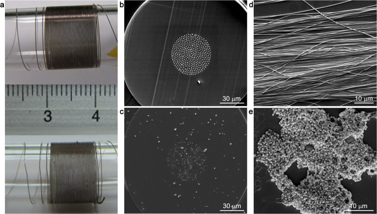
Heat treatment of PES-embedded nanowires does not compromise the structural integrity of the nanofiber, and indefinitely long arrays can be produced for any of the schemes described. In addition, the presence of the PES sheath renders the embedded nanostructure arrays sturdy enough to be handled directly (Figure 2a). Heat-modified nanostructures also retain the profiles of the initial nanowire (Figure 2b), but the out-of-phase alignment of parallel nanostructure arrays prevents the observation of all nanostructures on a single cross section (Figure 2c). The novel nanostructures also possess long-range alignment and high cross-sectional uniformity, which further increases their utility especially in nanophotonics applications. In addition, sheath-embedded core-shell configurations can be etched by dichloromethane (DCM) to produce free-standing core-shell nanostructure arrays (Fig. 2d, e), and core-only nanostructures can be fabricated by the removal of the shell region via plasma etching or exposure to PVDF-etching solvents (see Figure S2 for nanospring production by plasma etching). DCM-etched nanowires readily assemble into monolayers on glass surfaces, suggesting that the present method can also be utilized for the production of highly ordered single-layer nanostructure arrays (Figure S3).
Figure 2. Production of indefinitely long nanostructure arrays.
(a), A 2 m nanowire array converted into core-shell nanospheres, demonstrating that fibre integrity is not significantly altered by heat treatment, and that nanostructure arrays can be produced in macro-scale lengths by the present method. Cross-sectional images demonstrate that (b), nanowire phase alignment is not compromised following the production of (c), nanosphere arrays, but the out-of-phase alignment of parallel nanostructure arrays prevents the observation of all core features on a single cross-section. In addition to sheath-embedded arrays, core-shell (d), nanowires and (e), nanospheres can be fabricated following the etching of the PES polymer sheath.
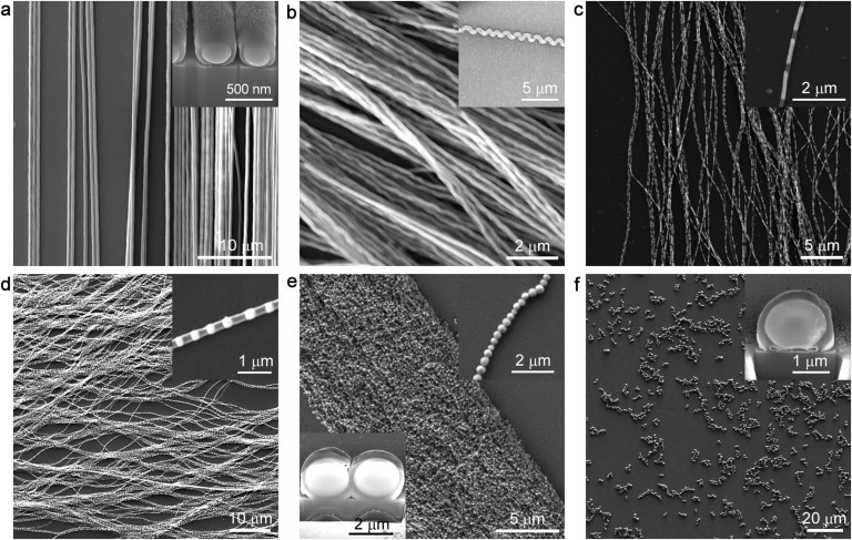
In-fiber nanostructures are characterized by SEM and FIB following the removal of the PES sheath by DCM etching (see Methods for details). SEM imaging reveals that large-area arrays can be obtained for each nanostructure configuration, and that uniform production of a specific scheme can be accomplished by fixing the process temperature (Figure 3a–f). Inter-structural distances and individual nanostructure lengths are determined by the wavelength of thermal instability which can be altered by changing the process temperature and duration (Figure S4). Precise size control of fabricated nanostructures is demonstrated in step II nanowires by physically restraining the initial wire during nanosphere formation at 300°C and considering mass conservation. “Taut” (i.e. restrained with no room for contraction) nanowires produce spheres with diameters comparable with the initial structure, while “slack” microfibers contract during the process and form nanospheres with larger diameters (Figure S5). We also demonstrate that the structures produced are suitable for applications requiring precise control over material morphology and uniform material distribution, by characterizing the cross-sectional uniformity of two 1.5 µm microchain links (Figure S6). The high regularity observed in the core region is particularly notable, which have a determinative effect especially on optical properties. This regularity is also reflected on the sizes of the produced nanoparticles (see e.g. Figure S7 for a histogram of shell-embedded nanorods, which possess standard deviation to diameter ratio of 7%).
Figure 3. Characterization of fabricated nanostructures.
Temperature-dependent structure formation observed by scanning electron microscopy. Fabricated nanostructures are etched by dichloromethane and dispersed on glass prior to imaging. (a), Nanowires can be converted into (b), nanosprings, (c), nanoshell-embedded rods, (d), nanopeapods, (e), nanochains and (f), core-shell nanospheres. Sizes of fabricated nanostructures depend on initial nanowire thickness and are 200–300 nm for all images. FIB was used to obtain representative cross-sectional images of fabricated nanowires, chains and core-shell spheres (inset).
Modelling of heat-induced transition
The formation of spheres via fluid instability is a well-attested and well-explained phenomenon31,32,33,34,35,36,37. However, models dealing with this phenomenon assume only the presence of radial and axial instabilities and do not consider existence of non-axisymmetrical occasions, such as that examplified by nanosprings. Helical shape formation is instead explained by purely mechanical models, as in the cases of gut formation38 and cucumber tendril coiling39. We present a fluid dynamics-based model to describe the formation of nano-springs and other unconventional nanoschemes, and utilize a two-dimensional simulation model to support our observations. In the course of the heat treatment process, nanosprings and rods form at relatively low temperatures (200–220°C), where the PES sheath acts as a rigid wall against the molten PVDF shell and the viscous As2Se3 core, and the molten shell region tends to minimize its surface energy by increasing its curvature. Our contact angle measurements (Figure S8) show that the PVDF-As2Se3 interfacial energy is smaller than that of the PVDF-PES interface. Consequently, the curvature formation leads to a greater increase in the interface area of PVDF-As2Se3 compared to the area of the PVDF-PES. Since the As2Se3 core is still highly viscous at low temperatures, formation of necks requires high energy to form in-phase PVDF arcs. Therefore, energetically less expensive PVDF arcs formation with axial phase shift are most favorable. This axial shift leads to formation of helices (non-axisymmetric instability case). Increasing temperature reduces core viscosity and enables that this shift reaches zero, hence the axisymmetric condition results in neck formation leading to shell embedded nanorod scheme and the further decrease in As2Se3 viscosity triggers an increase in the influence of the surface tension, hereby result in sphere formation.
Figure 4 shows the results of our simulations, which are performed for the characterization of core fragmentation but can also be extended to encompass the temperature range at which the shell region is also deformed. Our simulation results suggest that nanowire deformation is initiated by the formation of core-shell As2Se3-PVDF spirals at lower (205°C) temperatures (Video S1). Increasing the temperature to 215°C induces nanowire fragmentation and rod formation (Video S2), and at temperatures over 230°C resulting in the formation of nanospheres (see Figure 3c, d for the general morphology of nanorods and nanospheres) (Video S3). Theoretical calculation results are in line with our experimental observations (Figure 1). Nanowires can be induced to deform into any of the aforementioned nanostructures by using a suitable combination of temperature and process duration (Figure 4b). The phase diagram shows that nanosprings and nanorods can be obtained at lower temperatures and in narrow intervals of process parameters, while nanospheres can be obtained at relatively high temperatures and with a large process window. Transition regions represent transformations (Figure S9) between two regular shapes (e.g. the yellow transition region contains mixed phase of nanorods and nanospheres).
Figure 4. Numerical simulation of nanostructures.
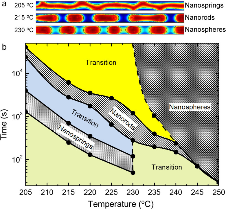
(a), COMSOL Multiphysics software is used for the modelling of core-region deformations. Formation of nanoschemes are simulated using the fluid instability phenomenon. Nanosprings are produced at low temperatures (215°C), where As2Se3 viscosity is very high. At higher temperatures, viscosity decreases and the glass core is broken up into a series of rods, while the production of nanopeapods is favored at temperatures around 230°C. (b), Process parameters controlling the formation of complex structures. Nanosprings and nanorods are not stable at very high temperatures, and complete nanospheres cannot be obtained at very low temperatures. Spline lines and straight lines are used to discriminate regions based on simulation results (points), while dotted lines represent an extrapolation for regions where the simulation does not converge. Transition regions correspond to intermediate stages of the formation of complete and regular nanostructure shapes.
Functionality of nanostructures
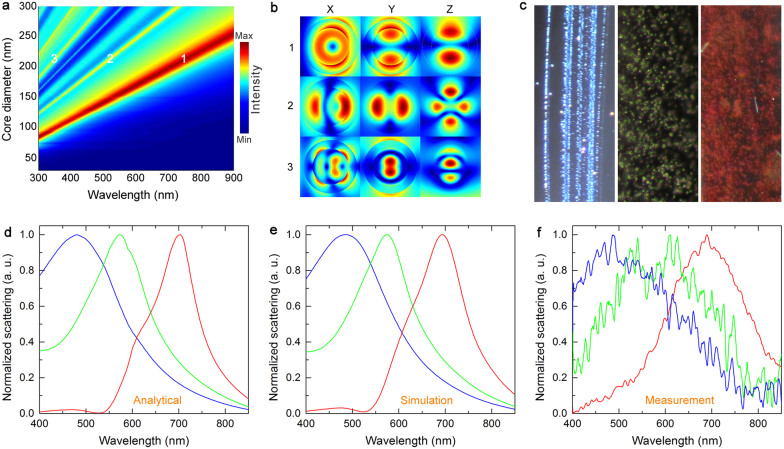
We also show the optical potential of our core-shell dielectric nanostructures by engineering a variety of different nanoschemes for size-dependent structural coloring. As nanospheres are well-characterized in Mie theory40,41,42 and find widespread application in nanoscale optics, here we concentrate on core-shell nanospheres and investigate their scattering properties. We utilize the first mode of resonant light scattering, which is independent of polarization and displays vivid hues with linear dependence on particle size (Figure 5a, b). Colored core-shell nanospheres span the whole visible spectrum within the size range of 100–250 nm, with larger sizes corresponding to higher wavelengths. The thermal basis of the fabrication technique results in a high uniformity and smoothness, which prevents size-dependent shifts in scattering spectra and allows the production nanosphere arrays displaying uniform large-area coloration. Experimental data are collected from large-area nanostructures and FDTD calculations are performed for nanospheres with average core diameters of 130 nm, 170 nm and 220 nm, corresponding to blue, green and red coloration, respectively (Figure 5c). We also model Mie scattering with analytical calculations based on Lorenz-Mie formalism, and find our FDTD calculations and analytical results to be in agreement for the diameter sizes tested (Figure 5d, e). In addition, experimental findings are in line with theoretical calculations if we ignore small variations associated with collective scattering from large area sphere arrays (Figure 5f).
Figure 5. Characterization of colored core-shell nanospheres.
(a), Scattering map describing the positions of the lower resonant modes. (b), Fields are localized inside the nanostructure and exhibit a leaky-mode resonant behavior. Nanostructure hues can cover the whole visible spectrum using the first resonant mode, with a linear dependence on size. (c), Large-area core-shell nanosphere arrays engineered for blue, green and red hues, with average diameters of c. 130, 170 and 220 nm, respectively. (d), Analytical solutions for light scattering from spherical core-shell nanostructures are modeled with Lorenz-Mie theory and overlap both with (e), FDTD simulation and (f), experimental scattering data measured by inverted dark-field microscopy. Collective scattering from large area spheres with narrow size distributions result in uniform coloration and small shifts in scattering spectra. Ellipsometric material parameters are used in FDTD and analytical calculations.
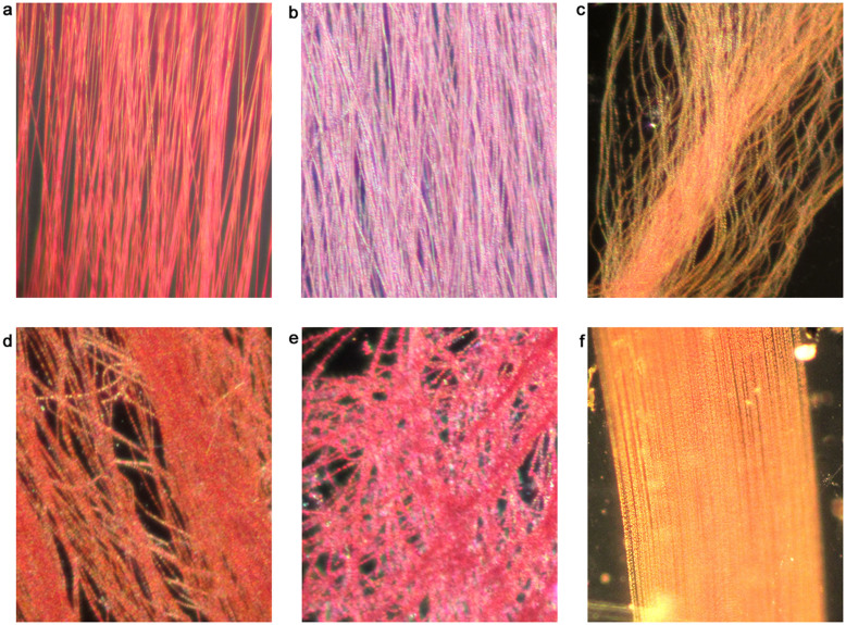
In addition to the characterization of core-shell nanospheres, we provide large-area coloration images (Figure 6) and numerical simulations for the intermediate structures (Figure S10), though we leave the detailed investigation of their properties outside the scope of this study. Large-area coloration of nanostructures produced by the combined ISR-thermal manipulation technique highlights a potential area of application for the fabrication method and first to configure large-area arrays of in-fiber nanospheres, nanosprings, shell-embedded nanorods, nanopeapods and nanochains for their optical functionality at the nanoscale. Any of the above-mentioned nanostructures can be produced as indefinitely long, colored arrays to be utilized as scattering ingredients in paints, functional textiles and color pixels in flexible display technology. In particular, in-fiber nanosprings may also be utilized to great effect in photonics topological insulators43 and photonic metamaterials44; while free-standing nanospring arrays may find applications in enhanced catalytic converters45, SERS substrates46, artificial olfaction47 and energy storage48. Embedded discrete rods and spheres may enable the fabrication of novel nanoantenna arrays49,50, and nanochains may find potential use in solar thermal absorbers51, luminescent platforms52 and single electron transistors53. Core-shell nanospheres can be used for a range of applications, including photonic crystal barcodes54 and sensing applications55. Further, many promising devices require the use of in-fiber nanomaterial arrays, and can be produced with ease using our proposed fabrication platform. These devices include dielectric metamaterials, dielectric nanoantenna, novel types of coupled nanowaveguides, novel nonlinear waveguides, nanoresonator arrays and functional nanobiomimetic devices incorporating novel optical interaction strategies.
Figure 6. Large-area coloration of nanostructures embedded in polymer matrix.
(a–f), Resonant Mie scattering-based coloration observed on various fabricated nanoschemes. High uniformity and smoothness is paramount for large-area coloration and may result in size dependent color shifts when compromised. Our fabrication method is able to achieve minimal variance in nanostructure diameters, and is not subject to such structural errors. Sizes are 200–300 nm for all cases.
Discussion
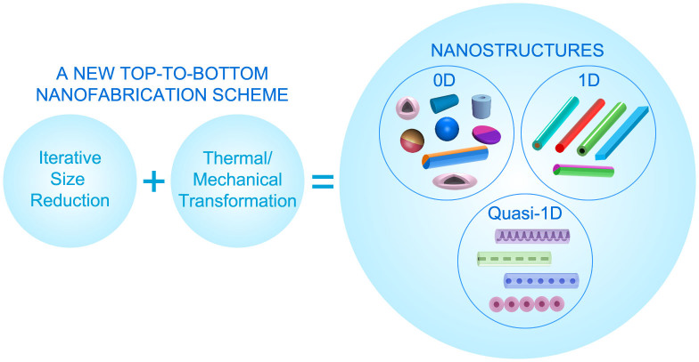
Our present investigations complement the existing methodology for the ISR-based production of complex nanostructures and render it possible to utilize such methods for the generation of a great variety of 0D/low aspect ratio, 1D and complex/quasi-1D nano-building blocks in indefinitely long, ordered arrays, the diversity of which can be further enhanced by mechanical transformation tools56,57 (Figure 7). In addition, the transition behavior associated with our As2Se3–PVDF core-shell nanowires is expected to be applicable to other material systems, and possibly to other fabrication techniques. In particular, as long as the core-shell components meet certain criteria (i.e. the materials are thermally compatible and their glass transition temperatures follow a well-defined pattern), this method can be extended to SiO2 glass-encapsulated Si, Ge, many metals (e.g. Ag, Fe), phase change materials and magnetic materials. In addition, many polymeric nanostructures can be obtained by using our technique. The controlled synthesis of such nanostructure arrays may allow their integration into larger, self-assembled metastructures closely matching the impressive and multi-faceted properties of biological nanostructures. ISR is particularly advantageous for the generation of macro-scale devices by nanomaterial assembly, as this low-cost, high-throughput process is capable of generating globally aligned, arbitrarily long nanostructures within a robust polymer sheath that circumvents handling issues associated with previous nanostructure platforms and allows the simple macroscopic manipulation of the composite fiber. The composite material is highly promising for the development of in-fibre nanodevices with significant advantages over on-chip devices, such as the ability to utilize flexible out of plane geometries in light weight, wearable and disposable devices. ISR-based methods also allow the convenient provision of an electrical current to single nanostructures and nanostructure arrays, which can be easily accomplished by directly connecting the fiber end facets to a source. In renewable energy applications, nanostructure-embedded fibres incorporated within large area photovoltaic devices can bridge the advantages of nanotechnology (e.g. high efficiency) with the requirements of large scale production. The basic capacity to produce single and multimaterial nanoarchitectures in flexible fibres is so general and powerful that it can open up whole new fields of basic and applied research and lead to a vast number of novel device designs.
Figure 7. Potential and implications of ISR-based device fabrication.
ISR-based methods provide a convenient means for the cheap, large-scale, straightforward fabrication of nanostructures. These methods rely on thermal basement and are highly complementary, allowing the production of a vast number of distinct nanoarchitectures in well-ordered arrays within indefinitely long fibers. Each type of nano building-block supplies a new series of features and conveniences for the generation of novel, highly efficient nanodevices.
Methods
Arsenic selenide (As2Se3) glass rod synthesis
As2Se3 rods, 4 mm in diameter and 8 cm in length, are prepared by melting in a vacuum-sealed quartz tube followed by water quenching. The weighted materials are placed in a quartz tube under nitrogen atmosphere in a glove box (H2O, O2 below 0.1 ppm). The quartz tube is kept at 330°C for a 2 hour under vacuum to remove surface oxides, sealed in a glass ampoule (10−6 Torr), rocked for 18 h at 600°C and quenched in iced water prior to use.
Macroscopic composite preparation, consolidation and thermal size reduction
The macroscopic preform for nanofiber fabrication is prepared in a clean pressure flow room by wrapping a PVDF polymer film (6 mm diameter) around As2Se3 glass rods (4 mm diameter), and subsequently wrapping a polyethersulphone (PES) film around the core-shell structure until a final diameter of 25 mm is obtained. The macroscopic fiber is then consolidated above the glass transition temperature of its components (260°C for 30 minutes, under a 10−3 Torr vacuum) and thermally drawn in a custom-built fiber tower, specifications of which can be found in Ref. 27. Briefly, the macroscopic structure is heated and drawn into 200 m of step I microwire in a vertical two-zone furnace, with a top zone temperature of 275°C and bottom zone temperature of 200°C. Drawing parameters such as drawing speed, down feed speed and temperature are controlled thorough the fabrication process. PES sheaths for step II nanowires are prepared by wrapping several layers of PES film around a Teflon-coated glass rod, consolidating the PES layers under 260°C and removing the Teflon-coated rod to create a hollow tubing of PES. 360 step I microwires (diameter = 0.4 mm, length = 10 cm) are then inserted into each PES sheath and drawn into step II nanowires, the diameters of which are controlled using a laser micrometer by monitoring total fiber diameter. Arbitrarily long nanowires can be produced in a broad diameter range (50–1000 nm) after step II, and the process can be repeated to obtain smaller diameters (e.g. 10 nm after a “step III”, identical to step II except with nanowires, instead of microwires, as the initial material). The overall reduction factor at the end of step II is 105.
Heat treatment of nanowire arrays
Prior to heat treatment, PES-embedded core-shell nanowire arrays are wrapped around a glass tube or placed on a glass substrate, with and without edge restriction. Edge restriction fixes the macroscopic structure and prevents the thermal contraction of the fiber during heat treatment, resulting in fabricated structures bearing diameters comparable with that of the original nanowire. Larger nanostructure diameters can also be obtained by restricting wire ends in “slack” lines to partially allow thermal contraction, or by using free-standing fibers. Heated fibers deform into nanosprings (205°C), shell-embedded discrete rods (215°C), shell-embedded spheres (230°C), nanochains (250°C) and core-shell nanospheres (270°C) with increasing temperatures (all values given are for 90 nm nanowire arrays treated for approx. 2 min., and increase for larger nanowire diameters). Production optimization is also performed for a fixed heating time (t = 10 s.) and nanowire thickness (d = 180 nm) to observe the transition between different nanoconfigurations.
Nanostructure extraction
Dichloromethane (DCM) (Carlo Erba) is utilized to etch the PES sheath covering the core-shell nanostructure arrays and expose the structures for electron microscopy imaging. PES-embedded nanostructure arrays are placed on a glass substrate, and the PES layer is etched by DCM drop cast directly onto the surface. The exposed nanostructures are rinsed gently with DCM to remove residual polymer. PVDF shells of core-shell nanostructures are highly resistant to DCM etching, and are not damaged during the nanostructure extraction process.
Fluid dynamic simulation:
A two dimensional numerical finite element method (FEM) simulations are performed using the COMSOL software for the modeling of heat-mediated nanostructure deformation. A level-set function  is coupled with Navier-Stokes equations58. The level-set function
  is defined as a signed distance function, where the interface between the two fluids is determined by the level-set function at
  = 0.5. The normal and curvature is determined from the level set function as
  and
and  , respectively. The coupled Navier-Stokes equation and the level-set function are simultaneously solved using the chemical engineering module in the COMSOL software.
Author Contributions
T.K. and M.B. designed and carried out research. O.T. performed the COMSOL simulations. T.K., M.B. and O.T. analyzed data and wrote the paper.
Supplementary Material
Supplementary document
Supplementary video 1
Supplementary video 2
Supplementary video 3
Acknowledgments
We would like to thank Alper D. Ozkan for his help in writing manuscript, critical reading of the manuscript and fruitful discussions, and Huseyin Duman for obtaining cross-sectional images with FIB. This work is supported by TUBITAK under the Project No. 110M412. The research leading to these results has received funding from the European Research Council under the European Union's Seventh Framework Programme (FP/2007-2013)/ERC Grant Agreement n. 307357.M.B. acknowledges partial support from the Turkish Academy of Sciences (TUBA).
References
- Natelson D. Nanofabrication: Best of both worlds. Nature Mater. 5, 853–854 (2006). [DOI] [PubMed] [Google Scholar]
- Gates B. D. et al. New approaches to nanofabrication: molding, printing, and other techniques. Chem. Rev. 105, 1171–1196 (2005). [DOI] [PubMed] [Google Scholar]
- Rogers J. A. & Paik U. Nanofabrication: Nanoscale printing simplified. Nature Nanotech. 5, 385–386 (2010). [DOI] [PubMed] [Google Scholar]
- Kawata S., Sun H.-B., Tanaka T. & Takada K. Finer features for functional microdevices. Nature 412, 697–698 (2001). [DOI] [PubMed] [Google Scholar]
- Kalantar-zadeh K. & Fry B. Characterization techniques for nanomaterials. Nanotechnology-Enabled Sensors, 211–281 (Springer, 2008). [Google Scholar]
- Lu W. & Lieber C. M. Nanoelectronics from the bottom up. Nature Mater. 6, 841–850 (2007). [DOI] [PubMed] [Google Scholar]
- Lieber C. M. & Wang Z. L. Functional nanowires. MRS Bull. 32, 99–104 (2007). [Google Scholar]
- Thelander C. et al. Nanowire-based one-dimensional electronics. Mater. Today 9, 28–35 (2006). [Google Scholar]
- Liu K. & Jiang L. Bio-inspired design of multiscale structures for function integration. Nano Today 6, 155-175 (2011). [Google Scholar]
- Yu Y., Zhang Q., Xie J. & Lee J. Y. Engineering the architectural diversity of heterogeneous metallic nanocrystals. Nature Commun. 4, 1454 (2013). [DOI] [PubMed] [Google Scholar]
- Sacanna S. et al. Shaping colloids for self-assembly. Nature Commun. 4, 1688 (2013). [DOI] [PubMed] [Google Scholar]
- Liddicoat P. V. et al. Nanostructural hierarchy increases the strength of aluminium alloys. Nature Commun. 1, 63 (2010). [DOI] [PubMed] [Google Scholar]
- Liu J. et al. The interesting influence of nanosprings on the viscoelasticity of elastomeric polymer materials: Simulation and experiment. Adv. Funct. Mater 23, 1156–1163 (2013). [Google Scholar]
- Varshney V. et al. A novel nano-configuration for thermoelectrics: helicity induced thermal conductivity reduction in nanowires. Nanoscale 4, 5009–5016 (2012). [DOI] [PubMed] [Google Scholar]
- Choi C. L. & Alivisatos A. P. From artificial atoms to nanocrystal molecules: Preparation and properties of more complex nanostructures. Annu. Rev. Phys. Chem. 61, 369–389 (2010). [DOI] [PubMed] [Google Scholar]
- Zeng Z. M. et al. GaP/GaOx core−shell nanowires and nanochains and their transport properties. J. Phys. Chem. C 112, 18588–18591 (2008). [Google Scholar]
- Cao G. Nanostructures and nanomaterials: synthesis, properties and applications (Imperial College Press, 2004). [Google Scholar]
- Vollath D. Nanomaterials: An introduction to synthesis, properties and application (Wiley-VCH, 2008). [Google Scholar]
- Ramasamya K. & Guptab A. Routes to self-assembly of nanorods. J. Mater. Res. 28, 1761–1776 (2013). [Google Scholar]
- Caputo G. & Pinna N. Nanoparticle self-assembly using π–π interactions. J. Mater. Chem. A 1, 2370–2378 (2013). [Google Scholar]
- Grzelczak M., Vermant J., Furst E. M. & Liz-Marzán L. M. Directed self-assembly of nanoparticles. ACS Nano 4, 3591–3605 (2010). [DOI] [PubMed] [Google Scholar]
- Merkel T. J. et al. Scalable, shape-specific, top-down fabrication methods for the synthesis of engineered colloidal particles. Langmuir 26, 13086–13096 (2010). [DOI] [PMC free article] [PubMed] [Google Scholar]
- Liang H. W., Liu S. & Yu S. H. Controlled synthesis of one-dimensional inorganic nanostructures using pre-existing one-dimensional nanostructures as templates. Adv. Mater. 22, 3925–3937 (2010). [DOI] [PubMed] [Google Scholar]
- Li D. & Xia Y. Electrospinning of nanofibers: Reinventing the wheel? Adv. Mater. 16, 1151–1170 (2004). [Google Scholar]
- Liu L. et al. Tailor-made inorganic nanopeapods: Structural design of linear noble metal nanoparticle chains. Angew. Chem. 120, 7112–7116 (2008). [DOI] [PubMed] [Google Scholar]
- Qin Y. et al. General assembly method for linear metal nanoparticle chains embedded in nanotubes. Nano Lett. 8, 3221–3225 (2008). [DOI] [PubMed] [Google Scholar]
- Yaman M. & Bayindir M. et al. Arrays of indefinitely long uniform nanowires and nanotubes. Nature Mater. 10, 494–501 (2011). [DOI] [PubMed] [Google Scholar]
- Khudiyev T., Ozgur E., Yaman M. & Bayindir M. Structural coloring in large scale core–shell nanowires. Nano Lett. 11, 4661–4665 (2011). [DOI] [PubMed] [Google Scholar]
- Ozgur E., Aktas O., Kanik M., Yaman M. & Bayindir M. Macroscopic assembly of indefinitely long and parallel nanowires into large area photodetection circuitry. Nano Lett. 12, 2483–2487 (2012). [DOI] [PubMed] [Google Scholar]
- Grillet C., Bian S. N., Magi E. C. & Eggleton B. J. Fiber taper coupling to chalcogenide microsphere modes. Appl. Phys. Lett. 92, 171109 (2008). [Google Scholar]
- Shabahang S., Kaufman J. J., Deng D. S. & Abouraddy A. F. Observation of the Plateau-Rayleigh capillary instability in multi-material optical fibers. Appl. Phys. Lett. 99, 161909 (2011). [Google Scholar]
- Kaufman J. J. et al. Structured spheres generated by an in-fiber fluid instability. Nature 487, 463–467 (2012). [DOI] [PubMed] [Google Scholar]
- Rayleigh L. On the capillary phenomena of jets. Proc. R. Soc. Lond. 29, 71–97 (1879). [Google Scholar]
- Tomotika S. On the instability of a cylindrical thread of a viscous liquid surrounded by another viscous fluid. Proc. R. Soc. London A 150, 322–337 (1935). [Google Scholar]
- Eggers J. & Dupont T. F. Drop formation in a one-dimensional approximation of the Navier-Stokes equation. J. Fluid Mech. 262, 205–221 (1994). [Google Scholar]
- Liang X., Deng D. S., Nave J.-C. & Johnson S. G. Linear stability analysis of capillary instabilities for concentric cylindrical shells. J. Fluid Mech. 683, 235–262 (2011). [Google Scholar]
- Deng D. S., Nave J.-C., Liang X., Johnson S. G. & Fink Y. Exploration of in-fiber nanostructures from capillary instability. Opt. Express 19, 16273–16290 (2011). [DOI] [PubMed] [Google Scholar]
- Savin T. et al. On the growth and form of the gut. Nature 476, 57–62 (2011). [DOI] [PMC free article] [PubMed] [Google Scholar]
- Gerbode S. J., Puzey J. R., McCormick A. G. & Mahadevan L. How the cucumber tendril coils and overwinds. Science 337, 1087–1091 (2012). [DOI] [PubMed] [Google Scholar]
- Fu Y. H. et al. Directional visible light scattering by silicon nanoparticles. Nature Commun. 4, 1527 (2013). [DOI] [PubMed] [Google Scholar]
- Person S. et al. Demonstration of zero optical backscattering from single nanoparticles. Nano Lett. 13, 1806–1809 (2013). [DOI] [PubMed] [Google Scholar]
- García-Etxarri A. et al. Strong magnetic response of submicron silicon particles in the infrared. Opt. Express 19, 4815–4826 (2011). [DOI] [PubMed] [Google Scholar]
- Rechtsman M. C. et al. Photonic Floquet topological insulators. Nature 496, 196–200 (2013). [DOI] [PubMed] [Google Scholar]
- Gansel J. K. et al. Gold helix photonic metamaterial as broadband circular polarizer. Science 325, 1513–1515 (2009). [DOI] [PubMed] [Google Scholar]
- Corti G. et al. Next generation nanospring-enhanced catalytic converters. Clean Technology, Hydrogen & Transportation, 267–270 (2010). [Google Scholar]
- Sai V. V. R. et al. Silica nanosprings coated with noble metal nanoparticles: Highly active SERS substrates. J. Phys. Chem. C 115, 453–459 (2011). [Google Scholar]
- Dobrokhotov V. et al. Towards the nanospring-based artificial olfactory system for trace-detection of flammable and explosive vapors. Sensor Actuat B-Chem 168, 138–148 (2012). [Google Scholar]
- Wu X. L., Liu Q., Guo Y. G. & Song W. G. Superior storage performance of carbon nanosprings as anode materials for lithium-ion batteries. Electrochem. Commun. 11, 1468–1471 (2009). [Google Scholar]
- Pellegrini G., Mattei G. & Mazzoldi P. Nanoantenna arrays for large-area emission enhancement. J. Phys. Chem. C 115, 24662–24665 (2011). [Google Scholar]
- Chen G. et al. Optical antenna effect in semiconducting nanowires. Nano Lett. 8, 1341–1346 (2008). [DOI] [PubMed] [Google Scholar]
- Wang X. et al. High-performance solution-processed plasmonic Ni nanochain-Al2O3 selective solar thermal absorbers. Appl. Phys. Lett. 101, 203109 (2012). [Google Scholar]
- Gu Z. et al. Luminescent GeO2/Zn2GeO4 hybrid one dimensional nanostructures. CrystEngComm 15, 2904–2908 (2013). [Google Scholar]
- Rafiq M. A. et al. Conduction bottleneck in silicon nanochain single electron transistors operating at room temperature. Jpn. J. Appl. Phys. 51, 5202 (2012). [Google Scholar]
- Zhao Y. et al. Multifunctional photonic crystal barcodes from microfluidics. NPG Asia Mater. 4, e25 (2012). [Google Scholar]
- Kuznetsov A. I. et al. Laser fabrication of large-scale nanoparticle arrays for sensing applications. ACS Nano 5, 4843–4849 (2011). [DOI] [PubMed] [Google Scholar]
- Murugan G. S., Wilkinson J. S. & Zervas M. N. Optical microdiscus resonators by flattening microspheres. Appl. Phys. Lett. 101, 071106 (2012). [Google Scholar]
- Aktas O. & Bayindir M. et al. A new route of fabricating on-chip chalcogenide microcavity resonator array. Adv. Opt. Mater., 10.1002/adom.201400072 (2014). [Google Scholar]
- Olsson E. & Kreiss G. A conservative level set method for two phase flow. J. Comput. Phys. 210, 225–246 (2005). [Google Scholar]
Associated Data
This section collects any data citations, data availability statements, or supplementary materials included in this article.
Supplementary Materials
Supplementary document
Supplementary video 1
Supplementary video 2
Supplementary video 3


