Abstract
A directly self-crystallized graphene layer with transfer-free process on arbitrary insulator by Ni vapor-assisted growth at growth temperatures between 950 to 1100°C via conventional chemical vapor deposition (CVD) system was developed and demonstrated. Domain sizes of graphene were confirmed by Raman spectra from ~12 nm at growth temperature of 1000°C to ~32 nm at growth temperature of 1100°C, respectively. Furthermore, the thickness of the graphene is controllable, depending on deposition time and growth temperature. By increasing growth pressure, the growth of graphite nano-balls was preferred rather than graphene growth. The detailed formation mechanisms of graphene and graphite nanoballs were proposed and investigated in detail. Optical and electrical properties of graphene layer were measured. The direct growth of the carbon-based materials with free of the transfer process provides a promising application at nanoelectronics.
Graphene, one of the most attractive research topics in modern science owing to its fascinating electrical properties, has been attracted much attention1,2,3. Its unique structure, two-dimensional honeycomb carbon lattice, enables high conductivity and transparency1,2,3,4. This material is thus potentially expected to become a transparent conductive layer5 in optoelectrical applications6,7,8,9 and thus stimulates a lot of studies on the synthetic growth methods to requisitely develop high uniformity with high quality and simple process for industrial manufactory3.
Common process for the synthesis of the graphene is typically based on heat chemical vapour deposition (CVD), for which carbon sources such as methane and acetylene are as precursors with metal-catalytic layers such as Cu or Ni foils10,11. However, an additional complex transferred processes of the graphene layer on an insulator substrate from the metal-mediated layer are imperative steps for the device application, containing spinning coating of protective layer, etching of mediated layer, fishing of graphene layer, and removal of protective layer. Defects, such as cracks, wrinkles, and chemical residuals (Fe3+, polymer…etc.) can be readily formed during transferred processes, resulting in decease of electron mobility due to scattering behaviours by defects, thereby degrading device performance12,13,14. Many transfer-free processes had been investigated to prevent these problems. The concept of back-side segregation by bulk or boundary diffusion had been applied to achieve the segregated graphene at interface between the substrate and the metal-mediated layer15,16,17. However, uncontrolled segregation of graphene at interface and additional removal of mediated layer makes mass production difficulty.
Other researches such as atomic layer deposition (ALD) or magnetically-enhanced arc discharge were used for direct deposition of graphene while limit quality of graphene and large scale production issues have to be taken into account18,19. Plasma-enhanced CVD (PECVD) or electron cyclotron resonance CVD (ECR-CVD) is alternative method for the direct growth of the graphene layer while crystallinity of graphene layer is needed to be improved20,21. In this regard, we demonstrate the direct growth of the graphene from the self-crystallization process without the transfer process on arbitrary insulator substrate by the Ni vapor-assisted growth at temperatures between 950 to 1100°C in a conventional heat chemical vapor deposition system, for which methane was used as the growth precursor. The thickness of the graphene with a maximum domain size of ~32 nm confirmed by Raman spectra can be controlled by the deposition time. By controlling different growth temperatures and pressures, growth of graphite nano-balls was found. The detailed formation mechanisms for the graphene and graphite nano-balls were proposed and investigated in detail. A sheet resistance of 3 kΩ/sq was measured for the single graphene layer (97%) at the growth temperature of 1000°C while the sheet resistance can be further decreased into 1 kΩ/sq and 0.6 kΩ/sq with transmittance of ~85 and ~70% at the growth temperature of 1050 and 1075°C, respectively. In addition, peak field effect mobilities for electron and hole were calculated to be in ranges between 180–200 and 170–200 cm2/V-s, respectively.
Results
Figure 1(a) shows schematic of how to directly grow graphene on a quartz substrate. Ni ingots with purity of 99.99% in a Al2O3 crucible was placed in the front of tube, followed by placing a quartz substrate at another end of the tube, with which the methane of ~50 sccm was used as the precursor. Forming gas, containing Ar/H2 with 100/20 sccm, was used to create a reduced atmosphere to prevent Ni ingots from oxidation during heating process. Therefore, the graphene layer can be directly grown on the quartz substrate without the metal-mediated layer at heating temperatures of 950–1100°C and pressures ranging from 60–360 torr. Figure 1(b) shows the corresponding Raman spectra at different growth temperatures with a fixed growth time of 5 min. Obviously, peaks at 1322 cm−1, 1597 cm−1, and 2645 cm−1 corresponding to D, G, and 2D bands were indexed. As the growth temperature decreases, the intensity of the D band increases, indicating that defect or boundary in the graphene increases22,23. Note that no growth of the graphene was achieved at growth temperature < 900°C or without Ni ingots even if the growth temperature researches to 1100°C (Figure S1). By using the equation, namely La(nm) = (2.4 × 10⁻¹⁰)λl4(ID/IG)−1, the average domain sizes of ~12, ~15, ~32 nm for graphene layers at growth temperatures from 1000, 1050, and 1100°C were calculated where λl, ID, and IG represent an excited wavelength when acquiring Raman spectra, intensity of D, and intensity of G band, respectively. Figure 1(c) shows an optical image of the graphene at 1100°C for 5 min. Although we only demonstrate a maximum size of 4 cm2 for the direct growth of the graphene owing to a limited diameter of 1 inch tube in our furnace system in present study, we believe that a larger scale area is achievable if larger size of the furnace is used. To shed light on how the uniformity of the graphene layer on the quartz substrate, Raman mapping images with a scanned area of 100 μm2 were measured as shown in Figures 1(c2) to 1(c5) and small scanned area of 25 μm2 were also shown in Figure S2. Obviously, uniform contrast in G and 2D mapping images reveals that the graphene is uniform (Figures 1c3 and c4). A mapping of IG/I2D as shown in Figure (c5) between 1 to 2.5 indicates multi-layer graphene23. Besides, we also discuss the distance dependence between the Ni ingots and the substrate from 10 to 30 cm at a fixed growth temperature and a pressure of 1100°C and 60 torr with methane and forming gas of H2 20 and Ar 100 sccm, respectively (Figure S3a). Interestingly, for distances of 10 to 30 cm between the Ni ingot and the substrate, the graphene grows with the identical quality confirmed by Raman spectra as shown in Figure S3(b), indicating a great potential of mass production with high uniformity. No graphene can be found if the distance of the Ni ingots and the substrate below 5 cm, which is most likely due to insufficient reaction time between the methane and the Ni vapour. Interestingly, the direct growth of the graphene from the self-crystallization process without the transfer process can be also applied on an Al2O3 substrate, demostrating the growth of the graphene on arbitrary insulator substrates by the Ni vapor-assisted growth in a conventional heat chemical vapor deposition system. (Figure S4).
Figure 1.
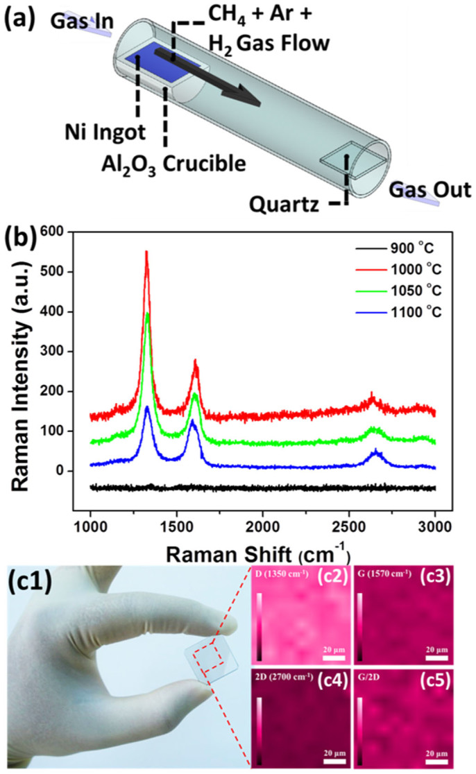
(a) A schematic of graphene grown by Ni ingot-assisted approach in the CVD system. (b) Corresponding Raman spectra at different growth temperatures from 1000 to 1100°C for 5 minutes, with which D band at 1322 cm−1 G band at 1597 cm−1, and 2D band at 2645 cm−1 were measured. (c1) A optical image of the graphene deposited at 1000°C for 5 minutes. Insets (c2–c5) show Raman mapping images of D, G, 2D band, and G/2D ratios with scanned area of 100 μm2, respectively. Scale bars of c2 to c4 are ranged from 0 to 120 and the scale bar of c5 is ranged from 0 to 5.
The thickness control is an issue for the growth of the graphene layer. In the conventional CVD approach, the precise controlling of the graphene layer from single to multiple layers in a same metal-mediated layer is difficult. For example, the graphene with single layer or few layers was usually achieved using Cu foil/film as the mediated layer while the growth of the graphene layer with multiple layers was usually synthesized by Ni foil/film as the mediated layer. As mentioned before, the direct growth of the graphene through the self-crystallization process highly relies on the growth temperature and time. To shed light on the precise thickness control of the graphene growth, the same growth time of 5 min but different growth temperatures of 1000 and 1100°C were conducted as shown in Figures 2(a) and 2(b), respectively. Graphene with 1–2 layers, corresponding to average thickness between 0.8–1.2 nm, can be achieved at the growth temperature of 1000°C for 5 min while a much thicker graphene with thickness of ~38.4 nm, corresponding to ~110 layers was obtained at the growth temperature of 1100°C for 5 min growth (Figure S5a). Note that the internal spacing of ~0.8 nm for the single graphene layer was observed while the internal spacing of each layer being 0.35 nm indicates multiple graphene layers with a sequential stacking along C-axis24. In addition, the thicknesses of graphene layers can be also controlled by changing the growth time from 5 to 180 min at the same growth temperature (Figure S5b). Furthemore, no Ni signal from TEM/EDS confirms the growth of the pure graphene as shown in table 1.
Figure 2.
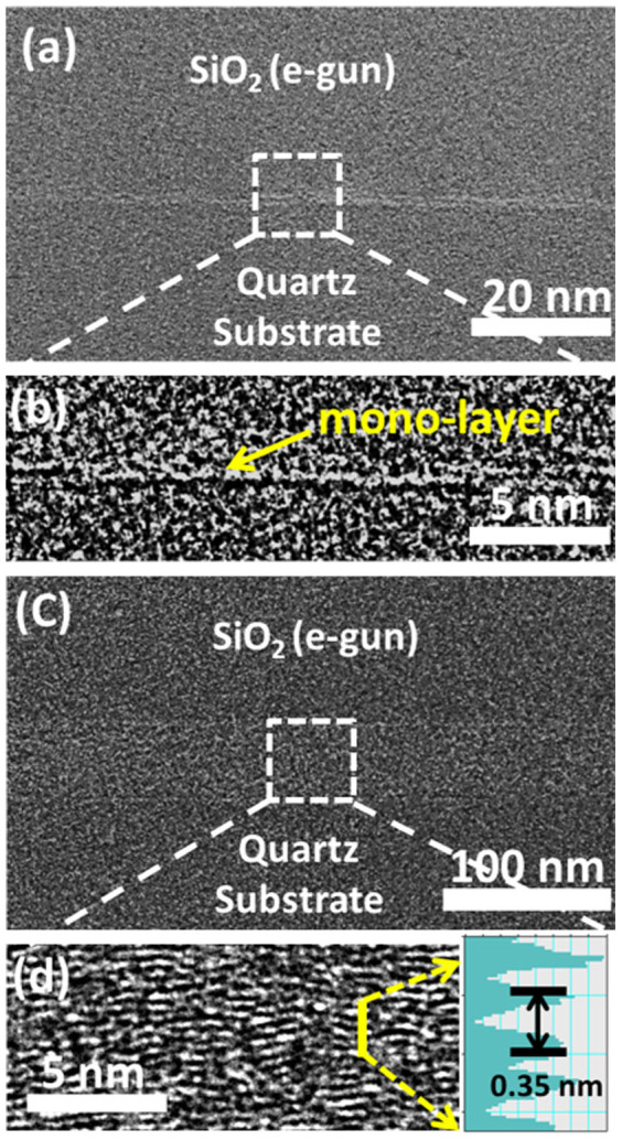
Low magnified TEM images of graphene deposted at (a) 1000 and (c) 1100°C sample for 5 minutes. The corresponding high resolution TEM images were shown in (b) and (d), respectively. Inset in (d) shows a internal layer distance of ~0.35 nm.
Table 1. EDS quantitative results for graphene and GNBs grown at 1000 and 1100°C for 5 minutes at 60 and 560 torr, respectviely.
| C K (at.%) | O K (at.%) | Ni K (at.%) | Total (at%) | |
|---|---|---|---|---|
| Graphene | 93.8 | 6.2 | 0 | 100 |
| GNBs | 99.3 | 0 | 0.7 | 100 |
X-ray photoelectron spectroscopy (XPS) was used to measure the bonding information in order to figure out the formation mechanism of the direct graphene growth as shown in Figure 3(a). For the graphene directly grown at 1100°C for 5 min, an obvious peak located at 284.4 eV was measured at the surface of the graphene, representing C-C sp2 bonding20. In addition, peak position slightly increases to 284.5 eV near to the surface of the quartz substrate due to a slight disordering near the quartz substrate contributted from the existence of lattice mismatch between the graphene and the quartz substrate at the intial growth20. To further unveil the quality of the C-axis crystallinity, internsity ratios of IG/I2D, the full width half maximum (FWHM) of 2D band which is convenient to assess both two-dimensional growth of graphitic layers, and three dimensional sequence of graphite lattice were used as shown in Figure 3(b)20,25,26,27. The FWHM of ~54.4 ± 7.3 cm−1 for the graphene grown at 1100°C with the growth time of ~5 min was measured while three references based on the direct growth of the graphene from literature reports were adopted for the comparison, respectively20,27,28. Obviously, the FWHM of the direct graphene growth in the present work exhibits the smallest value, indicating a better C-axis crystallinity than that of other approaches. In addition, internsity ratios of IG/I2D decrease from 3 to 1.2 as the grown temperature increases, suggesting that the thickness of the graphene, namely numbers of graphene layers, increases23. The increased thickness of the graphene is most likely due to the enhanced graphitization by self-crystallization process between methane and Ni clusters. Note that the deposition rate of the graphene increases with increase of the growth temperature. However, the_C-axis stacking sequence still remains.
Figure 3.
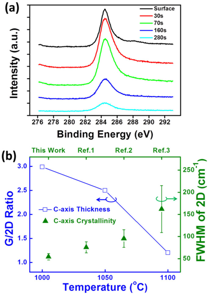
(a) XPS results of C-C sp2 bonding information at different depths, for which Ar ions were used to sputter the sample from surface to substrate. (b) G/2D ratios and full width at hall maximum (FWHM) as the function of the growth temperatures and crystallinity adopted from three references.
Interestingly, ball-like morphology, namely graphite nano-balls (GNBs), can be grown once the different working pressure was precisely controlled from 360 to 560 torr near an atmospheric pressure as shown in Figure 4(a). Inset in Figure 4(a) shows the corresponding Raman spectrum of GNBs. The peaks existed at 1334 nm−1 and 1598 nm−1 with respect to D and G bands were measured. The peak position of the G band is almost identical to that of the graphene while a shift to high energy state on D peak was observed, which is most likely resulted from partial formation of C-Ni bond at local areas22. The disappearance of the 2D band in the Raman spectrum is due to spherical shape without a preferred orientation from the continuous layer22. Notably, graphite cylinder shape, for example carbon nanotubes (CNTs), still exhibits the 2D band signal because the electron band structure does not split22. A low magnification TEM image in Figure 4(b) confirms the spherical shape of GNBs. Besides, the layer-by-layer configuration with an averagely internal d-spacing of ~0.37 nm, which is almost the same as the conventional multi-layer graphene, was observed by high resolution TEM image as shown in Figure 4(c) (Figure S6)29. We found that GNBs contains a slight amount of Ni clusters (0.7 at %) confirmed by the TEM/EDS analysis as shown in table 1. The growth temperature and the distance between the Ni ingots and the growth substrate significantly influence the diameter of GNBs rather than the morphology of GNBs. For example, the diameter of the GNBs decreases from 720 to 280 nm as the grown temperature decreases from 1100 to 900°C at the grown pressure of 560 torr and the distance of ~10 cm between the Ni ingots and the growth substrate (Figure S7a). Furthermore, increase of distances from 15 to 40 cm between the Ni ingots and the growth substrate can slightly decrease the diameter of the GNBs from 720 to 590 nm at the growth pressure and temperature of 560 torr and 1100°C, respectively (Figure S7b). A graphene with thick thickness on the substrate was grown prior to the formation of the GNBs (Figure S8), indirectly indicating that the growth of the GNBs is possibly achieved on the graphene during cooling process. It can be expected that that density of GBNs can be controlled by different cooling rates (air-cooling with cooling rate of ~20°C/s and furnace-cooling with cooling rate of ~0.3°C/s) where the reduced density of GNBs was observed under a lower cooling rate (~0.3°C/s) (Figure S9).
Figure 4.
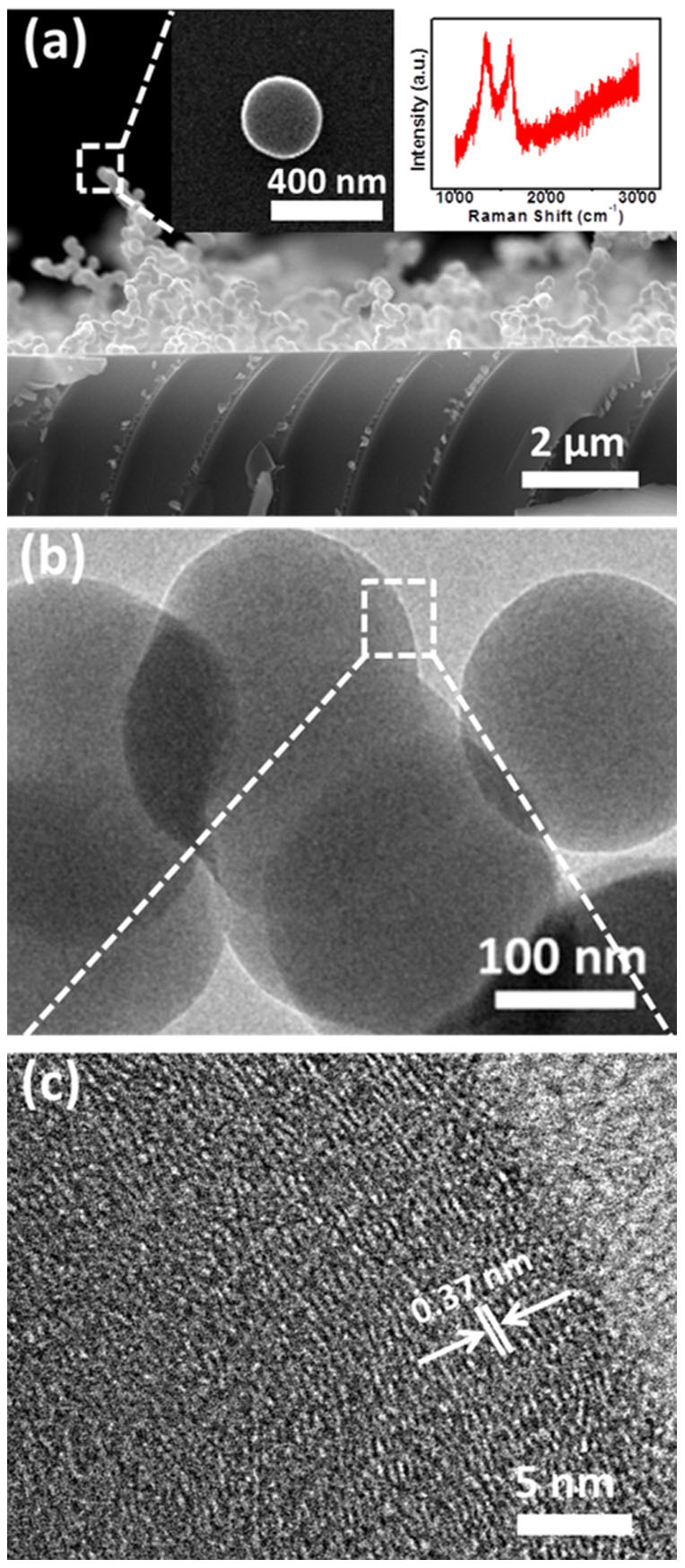
(a) A crossectional view of SEM image for GNBs grown at 950°C and 560 torr. Inset shows the corresponding Raman spectrum. (b) TEM image for GNBs in (a). (c) A high resolution TEM image for GNBs with a clearly internal layer distance of ~0.37 nm.
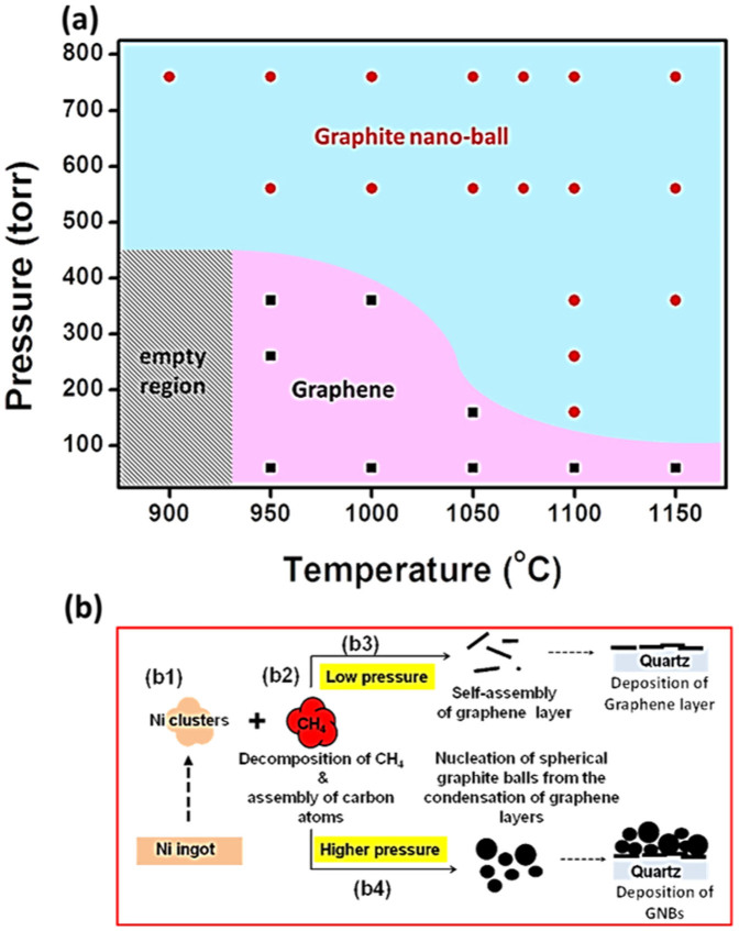
To understand the possible growth mechanisms of the graphene and GNBs, different growth pressures and temperatures were conducted at the identical substrate position of 10 cm away from Ni ingots as shown in Figure 5(a). Obviously, no either graphene or GNBs can be grown at a temperature lower than 900°C with a pressure less than 460 torr as indicated by gray area while the pure graphene growth without the formation of GNBs was achieved at temperatures higher than 950°C, with which the pressure has to be maintained in a low pressure as indicated by pink color area. Note that the critical pressure for the growth of the pure graphene decreases once the growth temperature increases. The growth of GNBs occurs if the pressures over the critical pressure (light blue color). Figure 5(b) shows schematics of how the graphene and the GNBs grow on the quartz substrate directly. Owing to the temperature used in the annealing process being much lower than melting point of Ni (1450°C), vaporous Ni atoms with a very lowpartial pressure ~10−8 psia (~10−4 torr) was possibly evaporated from solid Ni ingots30. The vaporous Ni atoms tend to aggregate with each other by reducing surface energy, resulting in formation of Ni clusters (Figure 5b1). The Ni clusters may not only trigger the decomposition of the methane (CH4) into carbon atoms but also initiate and accelerate the graphitization process by assembling carbon atoms into the graphene surrounding the Ni clusters, namely self-crystallization process (Figure 5b2). At low presure environment condition, the deposition of the graphene on the quartz substrate in terms of layer by layer growth is preferred while no Ni signal confirmed by TEM/EDS (table 1) and XRD (Figure S10) indicates that Ni clusters are most likely pumped out compeletely (Figure 5b3). Note that the uniform layer growth of the graphene regardless to the substrate position and distance with respect to Ni ingots indirectly indicates that the deposition of the graphene highly depends on the pressure while temperature difference only influences the graphene growth rate. Once the pressure increases, the deposition of the graphene remains while the thickness of the graphene is rather dependent of the pressure where the saturated thickness at the same growth temperature and time was observed as the pressure over 60 torr (Figure S11). However, the nucleation of the spherical shape occurs during the cooling down process, which is possibly resulted from the condensation of the graphene by Ni clusters or direct assembly of graphene during the cooling procress (Figure 5b4). The higher annealing temperature is, the fast growth rate of the graphene is. Consequently, the faster growth rate of the graphene also triggers larger nucleation size of GNBs during the cooling process in the higher pressure while the different cooling rates dominate the density of the GNBs. It is why the diameter of GNBs decreases with decreasing of growth temperature. It also explains that the larger diameter of GNBs syntheized on the graphene/quartz substrate approaching to Ni ingots was observed while the deposition of smaller diameter of GNBs usually was found at the longer distance between the Ni ingots and the growth substrate due to a longer diffusion length.
Figure 5.
(a)A statistic growth condition at different temperatures and pressure conditions on growth of graphene and GNBs. (b1–b4) Possible growth mechanisms of graphene and GNBs.
The direct growth of the graphene on the quartz substrate demonstrates a transfer-free process while optical and electrical properties are important issues for optoelectronics. Figure 6(a) shows a transmittance spectrum as the function of wavelengths for graphene with different layers deposited on 4 cm2 quartz substrates at different growth temperatures from 1000 to 1100°C for 5 minutes with a pressures of 60 torr and the Ar/CH4/H2 ratio of 100/50/20 sccm, respectively. Corresponding optical images at different growth temperatures with the identical growth time were shown in inset, respectively. For the growth temperature at 1000°C for 5 min, a single graphene layer was achieved (Figure 2b) with average transmittance of ~95% at visible wavelengths of 300–700 nm, which is consistent with a single graphene layer grown by CVD approach (97.3%) (Figure S12)31. The thickness of the graphene layer increases with the increased growth temperatures from 1000 to 1100°C, resulting in decrease in transmittance from 97 to 24%. In addition, sheet resistances as the function of growth temperatures were measured by four probes measurements as shown in Figure 6(b). A sheet resistance of 3 kΩ/sq was measured for the single graphene layer (97% transmittance) at the growth temperature of 1000°C, which is three time larger than that of the single graphene layer grown by CVD due to electron scattering by grain boundaries in graphene32. The sheet resistance can be further decreased into 1 kΩ/sq and 0.6 kΩ/sq with ~85 and ~70% in transmittance at the growth temperatures of 1050 and 1075°C for 5 min growth time, respectively, while the sheet resistance can be further reduced to 0.25 kΩ/sq at the increased temperature into 1100°C with the identical growth time (5 min).
Figure 6.
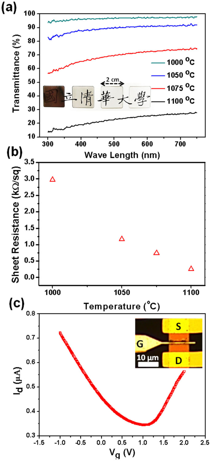
(a) Optical transmittance measurements from 300 to 750 nm for the graphene at different deposition temperatures. Inset shows optical images of the graphene deposited on quartz substrate at temperatures from 1000, 1050, 1075, and 1100°C for 5 minutes at 60 torr, respectively. (b) The corresponding sheet resistance in (a). (c) shows field effect transistor behaviors, with which single graphene grown at 1100°C for 5 minutes at 60 torr was used as a channel material. Inset shows the optical image, for which the channel length (L) of ~2 μm and channel width (W) of 5 μm can be observed, respectively.
To demonstrate the direct growth of the graphene used as channel material for electronic devices direcrly, the field effect transistor by a top-gate configuration on a quartz substrate through a self-oxidation process without the transfer process was also demonstrated (more details of the self-oxidation process, please see Figure S13)33,34. The graphene with micro ribbon shape was photolithographily patterned by an O2 plasma treatment. A 350 nm-thick Al layer deposited by E-beam evaporation was prepared as the gate electrode. The self-oxidation process was applied to achieve the gate dielectric layer with a dielectric capacitance of CTG = 1000 nF/cm2, followed by the formation of 0.5 nm Cr as a adhesion layer for 10 nm Au electrodes as source and drain29,30. The corrsesponding IDS-VGS behaviors and the optical microscopy image of device were shown in Figure 6(c) and inset. Obviously, Dirac point, at VGS = 1.1 V with VDS = 100 mV can be found, indicating that the graphene exhibits a slightly p-type nature, which might be due to the partial absorbance of oxygen molecules. In addition, the field effect mobility can be calculated from μeffect = gmL/VDSWCTG where gm, L, VDS, and CTG represent transconductance (dIDS/dVGS), channel length, source-drain bias, and capacitance, respectively. As a result, the peak field effect mobilities for electron and hole to be in ranges between 180–200 and 170–200 cm2/V-s were calculated by taking peak gm = 0.05 S, L = 1 μm, VDS = 100 mV, and CTG = 1000 nF, respectively. Although the field effect mobilities of electron and hole are not very high due to the surface phonon-carrier scattering from grain boundaries becase of small graphene grains26, the values are still better than that of other direct graphene growths and are still comparable with that of the graphene grown from the Cu foil by CVD with small grain domain sizes15,23,35. The direct growth of the carbon based materials with free of the transfer procress can provide promising applications at nanoelectronics.
Conclusions
We successfully demonstrated an easy and fast method to directly grow graphene through the self-crystallization process on the quartz substrate by Ni vapor-assisted growth in the conventional CVD system. The thickness of the graphene layer can be controlled by deposition time with the largest average domain size of ~32 nm confirmed by Raman spectra, exhibiting an excellent crystallinity along C-axis. Growth of graphene and graphite nano-balls can be precisely controlled by different growth temperatures and pressures, respectively. The detailed formation mechanisms for the graphene and graphite nanoballs were proposed and investigated. A sheet resistance of 3 kΩ/sq was measured for the single graphene layer (97%) at the growth temperature of 1000°C while the sheet resistance can be further decreased into 1 kΩ/sq and 0.6 kΩ/sq with transmittance of ~85 and ~70% at growth temperatures of 1050 and 1075°C, respectively. The lowest sheet resistance of 0.25 kΩ/sq can be achieved at the increased temperature into 1100°C. The peak field effect mobilities for electron and hole were calculated to be in ranges between 180–200 and 170–200 cm2/V-s, respectively.
Methods
Synthesis of graphene layer and graphite nanoballs
Ni ingots was evaporated into vapor state after annealing from room temperature to target temperatures (950 ~ 1100°C) with a mixed gas of 20 sccm H2 and 100 sccm Ar in the 1 inch diameter quartz tube. After the temperature was reached to the target temperature, the working pressure was increased to 60 to 360 torr by decreasing the pumping rate. CH4 with 50 sccm was introduced into the tube. After finishing the deposition, the CH4 and H2 was turned off and the cage of furnace was open. If the deposition pressure was higher than 360 torr, the total amount of Ni vapor is also increased. During the cooling process, the Ni vapor was captured by the cold tube and the Ni became work like a seed the synthesis graphene layers onto the out shell and formed the graphite nanoball.
Material characterization
The microstrucutres were examined by field emission transmission electron microscopy (FE-TEM, JEM-3000F, JEOL operated at 300 kV with point-to-point resolution of 0.17 nm) and atomic composition was analyzed by electron dispersive spectrometer (EDS). Meanwhile, the depth profile and the interfacial bonding state were examined by X-ray photoelectron spectroscopy, which was calibrated by Pt bottom electrode (XPS, Perkin Elmer Phi 1600 ESCA system, operated at 25 mA/15 kV). The field-effect transistor by the top-gate configuration on the quartz substrate through the self-oxidation process without transfer process was demonstrated directly. The single graphene layer with micro ribbon shape was defined by the photo lithography and patterned by O2 plasma treatment. A 350 nm-thick Al deposited by E-beam evaporation was prepared as the gate electrode by E-beam lithography process. A self-oxidation processes was applied to achieved gate dielectric layer with dielectric capacitance, CTG = 1000 nF/cm2, followed by the formation of 0.5 nm Cr/10 nm Au electrodes as source and drain by self-alignment processes. Align 1500 B analyzer was used to measure transistor behaviors, with which top-gate and source-drain baises at −2 to 2 and 100 mV, respectively.
Supporting information
Raman spectra for growth of graphene with and without Ni ingots; Raman mapping images for 10 μm2 cell; Raman spectra of graphene growth at different quartz substrate positions with respect to Ni ingots; The direct growth of the graphene from the self-crystallization process without the transfer process can be also applied on an Al2O3 substrate; A high resolution TEM image of graphen deposited at 1100°C and 60 torr for 5 minutes; Layer structure at out shell for GNB; A high resolution TEM image of GNBs; Controlled diameter of GNBs at different growth temperatures and distances between Ni ingots and quartz subatrate; A SEM image of graphene layer before the GNB growth; A SEM image for growth of GNBs at a low cooling rate; XRD results with grazing angle for GNBs, graphene, and Ni ingots, respectively; Transmittance at 550 nm of graphene grown at different temperatures; Fabrication processes of the self-oxidation process on graphen layer with top-gate configuriton; Supplementary information accompanies this paper at http://www.nature.com/scientificreports.
Author Contributions
W.C.Y., P.W.C. and Y.L.C. designed the experiment and analyzed the data. W.C.Y., Y.Z.C., J.H.H. and C.H.Y. performed the experiments including SEM, TEM, EDX, XPS, Raman and optical and electrical measurement. W.C.Y. and Y.L.C. co-wrote the paper. All the authors discussed the results and commented on the manuscript.
Supplementary Material
Supplementary Information
Acknowledgments
The research was supported by the Ministry of Science and Technology through grants no, 101-2112-M-007-015-MY3, 101-2218-E-007-009-MY3, 102-2633-M-007-002, and the National Tsing Hua University through Grant no. 102N2022E1. Y.L. Chueh greatly appreciates the use of facility at CNMM, National Tsing Hua University through Grant no. 102N2744E1.
References
- Novoselov K. S. et al. Electric field effect in atomically thin carbon films. Science 306, 666–669 (2004). [DOI] [PubMed] [Google Scholar]
- Novoselov K. S. et al. Two-dimensional gas of massless Dirac fermions in graphene. Nature 438, 197–200 (2005). [DOI] [PubMed] [Google Scholar]
- Geim A. K. & Novoselov K. S. The rise of graphene. Nat. Mater. 6, 183–191 (2007). [DOI] [PubMed] [Google Scholar]
- Blake P. et al. Graphene-based liquid crystal device. Nano Lett. 8, 1704–1708 (2008). [DOI] [PubMed] [Google Scholar]
- Li X. et al. Transfer of Large-Area Graphene Films for High-Performance Transparent Conductive Electrodes. Nano Lett. 9, 4359–4363 (2009). [DOI] [PubMed] [Google Scholar]
- Wang X., Zhi L. & Mullen K. Transparent Conductive Graphene Electrodes for Dye-Sensitized Solar Cells. Nano Lett. 8, 323–327 (2008). [DOI] [PubMed] [Google Scholar]
- Wu J. et al. Organic Solar Cells with Solution-Processed Graphene Transparent Electrodes. Appl. Phys. Lett. 93, 263302 (2008). [Google Scholar]
- Han T. H. et al. Extremely Efficient Flexible Prganic Light-Emitting Diodes with Modified Graphene Anode. Nat. Phontonic 6, 105–110 (2012). [Google Scholar]
- Wu J. et al. Organic Light-Emitting Diodes on Solution-Processed Graphene Transparent Electrodes. ACS Nano 4, 43–48 (2010). [DOI] [PubMed] [Google Scholar]
- Li X. et al. Large-Area Synthesis of High-Quality and Uniform Graphene Films on Copper Foils. Science 324, 1312–1314 (2009). [DOI] [PubMed] [Google Scholar]
- Yu Q. et al. Graphene segregated on Ni surfaces and transferred to insulators. Appl. Phys. Lett. 93, 113103 (2008). [Google Scholar]
- Li X. et al. Transfer of Large-Area Graphene Films for High-Performance Transparent Conductive Electrodes. Nano Lett. 9, 4359–4363 (2009). [DOI] [PubMed] [Google Scholar]
- Lin Y.-C. et al. Clean Transfer of Graphene for Isolation and Suspension. ACS Nano 5, 2362–2368 (2009). [DOI] [PubMed] [Google Scholar]
- Lin Y.-C. et al. Graphene Annealing: How Clean Can It Be? Nano Lett. 12, 414–419 (2011). [DOI] [PubMed] [Google Scholar]
- Su C.-Y. et al. Direct Formation of Wafer Scale Graphene Thin Layers on Insulating Substrates by Chemical Vapor Deposition. Nano Lett. 11, 3612–3616 (2011). [DOI] [PubMed] [Google Scholar]
- Yan Z. et al. Growth of Bilayer Graphene on Insulating Substrates. ACS Nano 5, 8187–8192 (2011). [DOI] [PubMed] [Google Scholar]
- Peng Z., Yan Z., Sun Z. & Tour J. M. Direct Growth of Bilayer Graphene on SiO2 Substrates by Carbon Diffusion through Nickel. ACS Nano 5, 8241–8247 (2011). [DOI] [PubMed] [Google Scholar]
- Wang X., Tabakman S. M. & Dai H. Atomic Layer Deposition of Metal Oxides on Pristine and Functionalized Graphene. J. Am. Chem. Soc. 130, 8152–8153 (2008). [DOI] [PubMed] [Google Scholar]
- Wu Z.-S. et al. Field Emission of Single-Layer Graphene Films Prepared by Electrophoretic Deposition. Adv. Mater. 21, 1756–1760 (2009). [Google Scholar]
- Medina H. et al. Metal-Free Growth of Nanographene on Silicon Oxides for Transparent Conducting Applications. Adv. Funct. Mater. 22, 2123–2128 (2012). [Google Scholar]
- Wang J. J. et al. Free-standing subnanometer graphite sheets. Appl. Phys. Lett. 85, 1265–1267 (2004). [Google Scholar]
- Ferrari A. C. & Basko D. M. Raman spectroscopy as a versatile tool for studying the properties of graphene. Nat. Nano. 8, 235–246 (2013). [DOI] [PubMed] [Google Scholar]
- Ferrari A. C. et al. Raman spectrum of graphene and graphene layers. Phys. Rev. Lett. 97, 187401 (2006). [DOI] [PubMed] [Google Scholar]
- Cancado L. G. et al. General equation for the determination of the crystallite size Laaof nanographite by Raman spectroscopy. Appl. Phys. Lett. 88, 163106 (2006). [Google Scholar]
- Lee C., Wei X., Kysar J. W. & Hone J. Measurement of the Elastic Properties and Intrinsic Strength of Monolayer Graphene. Science 321, 385–388 (2008). [DOI] [PubMed] [Google Scholar]
- Lespade P., Marchand A., Couzi M. & Cruege F. Caracterisation de materiaux carbones par microspectrometrie Raman. Carbon 22, 375–385 (1984). [Google Scholar]
- Rümmeli M. H. et al. Direct Low-Temperature Nanographene CVD Synthesis over a Dielectric Insulator. ACS Nano 4, 4206–4210 (2010). [DOI] [PubMed] [Google Scholar]
- Sun J., Lindvall N., Cole M. T., Teo K. B. K. & Yurgens A. Large-area uniform graphene-like thin films grown by chemical vapor deposition directly on silicon nitride. Appl. Phys. Lett. 98, 252107 (2011). [Google Scholar]
- Wallace P. R. The Band Theory of Graphite. Phys. Rev. 71, 622–634 (1947). [Google Scholar]
- Yaws C. L. Hand Book of Vapor Pressure. Gulf Publishing Company 4, 202–202 (1995). [Google Scholar]
- Nair R. R. et al. Fine Structure Constant Defines Visual Transparency of Graphene. Science 320, 1308 (2008). [DOI] [PubMed] [Google Scholar]
- Reina A. et al. Large Area, Few-Layer Graphene Films on Arbitrary Substrates by Chemical Vapor Deposition. Nano Lett 9, 30–35 (2009). [DOI] [PubMed] [Google Scholar]
- Lu C.-C., Lin Y.-C., Yeh C.-H., Huang J.-C. & Chiu P.-W. High Mobility Flexible Graphene Field-Effect Transistors with Self-Healing Gate Dielectrics. ACS Nano 6, 4469–4474 (2012). [DOI] [PubMed] [Google Scholar]
- Chen J.-H., Jang C., Xiao S., Ishigami M. & Fuhrer M. S. Intrinsic and extrinsic performance limits of graphene devices on SiO2. Nat. Nano. 3, 206–209 (2008). [DOI] [PubMed] [Google Scholar]
- Levendorf M. P., Ruiz-Vargas C. S., Garg S. & Park J. Transfer-Free Batch Fabrication of Single Layer Graphene Transistors. Nano Lett. 9, 4479–4483 (2009). [DOI] [PubMed] [Google Scholar]
Associated Data
This section collects any data citations, data availability statements, or supplementary materials included in this article.
Supplementary Materials
Supplementary Information


