

Abstract
Semiconductor nanocrystals are promising for use in cheap and highly efficient solar cells. A high efficiency can be achieved by carrier multiplication (CM), which yields multiple electron-hole pairs for a single absorbed photon. Lead chalcogenide nanocrystals are of specific interest, since their band gap can be tuned to be optimal to exploit CM in solar cells. Interestingly, for a given photon energy CM is more efficient in bulk PbS and PbSe, which has been attributed to the higher density of states. Unfortunately, these bulk materials are not useful for solar cells due to their low band gap. Here we demonstrate that two-dimensional PbS nanosheets combine the band gap of a confined system with the high CM efficiency of bulk. Interestingly, in thin PbS nanosheets virtually the entire excess photon energy above the CM threshold is used for CM, in contrast to quantum dots, nanorods and bulk lead chalcogenide materials.
 Carrier multiplication processes, where photons are converted into multiple charge carriers, promise higher efficiencies for solar cells based on quantum dots and nanorods. Here, the authors demonstrate carrier multiplication in PbS nanosheets, extending this effect to two-dimensional materials.
In semiconductors, photoexcitation leads to formation of an electron in a conduction band state and a hole in a valence band state. The electron–hole (e–h) pair initially has an excess energy equal to the difference between the photon energy and the band gap. The charges can lose their excess energy by cooling to states at the band edge via electron–phonon scattering. A hot charge carrier with excess energy larger than the band gap may also relax by exciting another electron across the band gap. The latter process is known as carrier multiplication (CM): the transition from a hot charge carrier state to an energetically equivalent trion state1. The trion consists of a charge carrier at lower energy and an additional e–h pair. CM competes with electron–phonon scattering until the hot charge carrier has cooled below the CM threshold. The competition between CM and inelastic electron–phonon scattering determines the final number of e–h pairs that are produced. The quantum yield of CM is defined as the number of e–h pairs produced per absorbed photon. An e–h pair in a trion can recombine by transferring the excitation energy to the third charge. This process is the inverse of CM and is known as Auger recombination2. In strongly confined semiconductor nanocrystals, Coulomb interactions are enhanced with respect to bulk, leading to an increased coupling between a single hot carrier and a trion. This makes carrier–trion interconversion processes much more efficient in confined structures than in bulk semiconductors3.
Much attention has been paid to how nanocrystal shape affects CM4,5. The extent to which a hot charge carrier undergoes the CM process is determined by the following factors: first, the Coulomb coupling strength between the hot charge and the equally energetic trion, which also depends on the dielectric constant of the environment6,7; second, the density of final trion states that are coupled to the initial hot charge carrier state; and third, the dephasing between the hot charge carrier state and the trion states5,8,9. The influence of all these factors on the CM process, as well as on the competing decay of hot charge carriers by electron–phonon cooling, varies with nanocrystal dimensionality and size. The demonstration of CM in quantum dots and nanorods of lead chalcogenides is of interest, since their band gap can be tuned to 0.7–0.9 eV, which is optimal to exploit CM in solar cells10.
In this Article, we show that for thin PbS nanosheets of 4 nm thickness, the photon energy in excess of the CM threshold is virtually completely used to produce additional e–h pairs, in contrast to quantum dots (zero-dimensional, 0D)11,12,13,14, nanorods (one-dimensional, 1D)15,16,17 and bulk (three-dimensional, 3D)18. The threshold energy of CM in PbS nanosheets with thickness in the range 4–7 nm is near 3 eV.
Results
Synthesis and structural characterization
PbS nanosheets, passivated by an oleic acid ligand layer, were synthesized according to a recently developed method19. Thin-film samples were prepared by drop-casting the nanosheets from toluene onto a quartz substrate. Details on the synthesis can be found in the Methods section. The nanosheet thickness as obtained from atomic force microscopy (AFM; 3±1, 5±1 and 6±1 nm) is close to that obtained from X-ray diffraction through the Scherrer equation (4.0±0.1, 5.9±0.1, 7.0±0.1 nm, respectively). Supplementary Fig. 1 shows representative transmission electron microscopy and AFM images of nanosheets. In this Letter we refer to the thickness as obtained from the X-ray diffraction measurements.
The absorption threshold of the nanosheets is blue-shifted with respect to bulk (Eg,bulk=0.41 eV20), as can be seen in the absorption spectra in Fig. 1. The blue shift is because of quantum confinement of e–h pairs in the direction perpendicular to the plane of the nanosheet. The transitions at 620 nm (2.0 eV) and 390 nm (3.2 eV) correspond to the bulk-like E1 and E2 transitions21, in close analogy to PbSe quantum wells22.
Figure 1. Steady-state optical absorption and transient bleach of 4- and 5.9 nm thick PbS nanosheets.

Steady-state absorption spectra of PbS nanosheets with a thickness of 4.0 and 5.9 nm. Inset: steady-state absorption spectrum (left axis) and maximum transient absorption signal ΔTmax/T for various probe wavelengths at constant pump fluence (black squares, right axis) for the 4 nm thick nanosheets.
Decay kinetics of photoexcited states
The dynamics of photogenerated electrons and holes was measured with two different time-resolved laser pump-probe optical absorption facilities (cfr. Methods). After photoexcitation, electrons and holes become thermalized near the band gap with an energy spread of about 25 meV (≈kBT at room temperature). These electrons and holes cause a bleach of the optical absorption near the band gap. The resulting increased transmittance of probe photons with energy near the band gap corresponds to a positive transient bleach signal, defined as ΔT/T=(Ton−Toff)/Toff. The inset of Fig. 1 shows the transient bleach signal for PbS nanosheets with a thickness of 4.0 nm as a function of probe wavelength. The shape and width of the bleach feature is because of the thermal energy distribution of charges and the energies of the optical excitations that are bleached, as well as the dispersion in nanosheet thickness. In what follows we refer to the band gap of the nanosheets as the photon energy at which the transient bleach is maximum, which is 0.83, 0.64 and 0.56 eV for nanosheets with thicknesses of 4.0, 5.9 and 7.0 nm, respectively. The band gap of 0.83 eV for the thinnest nanosheets is optimal to exploit CM in solar cells10.
Figure 2 shows the transient bleach signal (left axis) obtained by exciting PbS nanosheets with 800 nm pump pulses and probing at a photon energy near the band gap. In the first picosecond after photoexcitation, the bleach rises because of cooling of initially hot charge carriers to the band edge. The subsequent signal decay is because of recombination and possibly trapping of charges. The right axis displays the average density of e–h pairs in the PbS nanosheets. It was calculated by dividing the absorbed photon fluence by the total thickness of PbS material in the thin-film sample, which is estimated from the absorbance and the PbS bulk absorption coefficient23. The mono-exponential decay at the lowest pump fluence is typical for first-order decay of e–h pairs via geminate recombination or quenching at defects. The faster decay at higher fluences is due to Auger recombination of electrons and holes. The decay kinetics was globally fitted with the analytical solution to the differential equation for first- and second-order decay, (dn)/(dt)=−k1n−k2n2, with n the (e–h) pair density, k1=1.1 ns−1 the first-order decay rate and k2=2.5 × 10⁻²² cm3ps−1 the second-order Auger recombination rate.
Figure 2. Charge carrier decay kinetics.

Transient bleach traces (dots) for 5.9 nm thick PbS nanosheets excited at 800 nm at various pump fluences and probed at a photon energy for which the transient bleach is maximum. The pump fluences used yield e–h pair densities from 3.7 × 1017 cm−3 up to 1.8 × 1019 cm−3. Lines represent a global fit of the model with second-order Auger recombination, as discussed in the text.
The high quality of the global fit (hardly discernible from the experimental data) shows that Auger recombination follows second-order decay kinetics, which is typical for tightly bound e–h pairs that move together in the form of neutral excitons24,25. In the PbS dimensional extremes of 3D bulk and 0D quantum dots, electrons and holes do not pair up, and therefore decay via third-order Auger recombination24.
Determination of quantum yield
The maximum in the transient bleach, occurring at 3 ps after photoexcitation (corresponding to the cooling time of hot excitons), increases linearly with the absorbed pump laser fluence, or equivalently the exciton density, if higher-order Auger recombination is insignificant on this timescale. In the latter case, the exciton density can be determined from the maximum transient bleach, similar to previous transient terahertz conductivity measurements on bulk PbS and PbSe18, and time-resolved microwave conductivity measurements on PbSe QD films26.
Figure 3 shows the maximum transient bleach signal ΔTmax/T for various pump laser fluences and photon energies for the 5.9 nm thick PbS nanosheets. Similar data for the other nanosheet samples are shown in Supplementary Fig. 2 (4 nm thickness) and Supplementary Fig. 3 (7 nm thickness). The linear increase in ΔTmax/T with pump fluence reflects that the maximum in the transient bleach is directly proportional to the density of excitons and that higher-order exciton decay is negligible during the first 3 ps after the pump pulse. The relative uncertainty in ΔTmax/T is determined by the noise in transients as those in Fig. 2, and amounts to 1%. The maximum transient bleach signal ΔTmax/T depends linearly on the number of e–h pairs per absorbed photon (that is, the quantum yield), Φ, the pump photon fluence, I0, and the fraction absorbed pump photons, FA, according to
Figure 3. Determination of the variation of the quantum yield with photon energy.

Maximum bleach signal ΔTmax/T versus absorbed pump fluence at various pump photon energies for 5.9 nm thick PbS nanosheets. The solid line characterizes unit quantum yield, Φ=1. Steeper slopes imply higher quantum yields.
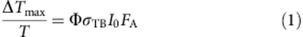 |
The value of transient bleach cross-section σTB=1.7±0.1 × 10⁻¹⁵ cm2 was determined from the value of ΔTmax/T obtained by photoexcitation with a known number of absorbed photons per unit area, I0FA, at low photon energy of 0.95 eV for which CM is energetically impossible and hence Φ=1. Note that the transient bleach cross-section σTB is not to be identified with the steady-state absorption cross-section (in the case of negligible spectator shift the latter is a factor g/2 larger, with g being the degeneracy of the band edge exciton)27. From equation 1 it follows that the derivative of ΔTmax/T versus I0FA scales with the quantum yield Φ. The three lowest pump photon energies coincide on a unique line characterized by unit quantum yield. The slope increases for the highest three pump photon energies, implying an increasing quantum yield, reaching a quantum yield of up to 2.2 after exciting with 4.66 eV pump photons. Numerical values of the quantum yield are given in the legend of Fig. 3.
Discussion of CM efficiency
Figure 4a shows a plot of the quantum yield Φ versus pump photon energy hν for three PbS nanosheet samples; that is, for each nanosheet a fluence set of data as in Fig. 3 is converted to a single data point in Fig. 4. The relative uncertainty in the quantum yields in Fig. 4 is at most 8% and is because of the uncertainty in the fraction of pump light absorbed, FA(2%), the noise in the photobleaching transients ΔTmax/T (1%) and the incident pump fluence, I0(5%)—see Methods section. In addition, displayed in the figure are recent literature data on PbS quantum dots12,13 and bulk PbS18. For the quantum dots, care was taken to select only data from experiments that were properly flowed or stirred, to avoid artificially high quantum yields or low thresholds for CM28. Interestingly, the CM threshold has the same value of hvth=3 eV for the three nanosheet samples, despite the different thickness and band gap. This threshold is similar to that reported for PbS quantum dots, which after conversion to photon energy are found to be near 3 eV12,13. This threshold is significantly higher than in bulk PbS (hvth≈2.3 eV)18. Further studies are needed to elucidate why the threshold for bulk differs from that of nanocrystals, for which the threshold does not depend on dimensionality or size. Above the threshold, the quantum yield for PbS nanosheets increases with photon energy as 0.95±0.15 eV−1. This CM efficiency (that is, dΦ/d(hν)) is comparable to bulk PbS and is significantly higher than that for PbS quantum dots (0.3 eV−1)12,17,18. We believe that the dimensional trends of CM threshold and CM efficiency have their origin in the band structure and the influence of quantum confinement on the discretization of wave vectors. Above the CM threshold, the efficiency of CM we find for two-dimensional (2D) nanosheets is similar to bulk, and much higher than for quantum dots and rods. This might be related to the fact that the discretization of wave vector states in confined systems severely limits the available trion states that can couple to the hot exciton. It appears that 2D nanosheets provide an optimum combination of an enhanced band gap due to quantum confinement perpendicular to the plane of the sheet with a high density of states due to spatial extent of electronic states in the plane of the sheet.
Figure 4. Comparison of quantum yield in PbS quantum dots, bulk and nanosheets.

Quantum yield Φ plotted versus (a) pump photon energy hν, or (b) band gap multiple hν/Eg, for PbS nanosheets with thicknesses as indicated. The uncertainties in the quantum yields have been determined as described in the text and in the Methods section. In addition displayed is recent literature data on obtained quantum yields in PbS bulk and quantum dots. In b the slope of the data points is equal to the CM efficiency ηcm (solid lines).
For solar cell applications, the number of e–h pairs produced per unit photon energy normalized to the band gap Eg is usually considered as the appropriate measure of CM efficiency. According to this, the normalized CM efficiency is ηcm≡Eg(dΦ)/(d(hν))29. Figure 4b shows the quantum yield versus the photon energy normalized to the band gap, together with the values of ηcm obtained from the slopes of linear fits to the data above the CM threshold. The normalized CM efficiencies range from ηcm=0.9±0.15 for the thinnest nanosheets (d=4 nm) to ηcm=0.55±0.10 for the thicker nanosheets. For the thinnest nanosheets, ηcm is close to 1, which implies that virtually all photon energy in excess of the CM threshold is converted into additional e–h pairs. The value for the thinnest nanosheets is significantly higher than the results for ηcm in lead chalcogenide quantum dots, nanorods and bulk, which are in the range 0.3–0.512,17,18.
The normalized CM efficiency in 2D PbS nanosheets is higher than previously published results for 0D quantum dots, 1D nanorods and 3D bulk. In 4 nm thick PbS nanosheets, almost all photon energy in excess of the CM threshold is converted into excitation of additional e–h pairs. The CM threshold near 3 eV in PbS nanosheets is similar to that for quantum dots. It should be noted, however, that the fraction of solar photons with energy above this threshold energy is small. This makes these nanosheets of limited practical use for exploitation of CM in solar cells. Further studies are needed to combine the near maximum CM efficiency in 2D nanosheets with a lower threshold energy.
Methods
Synthesis of PbS nanosheets
The PbS nanosheets were synthesized according to a previously published method19. The procedures used in the synthesis were slightly varied in order to produce the three samples with different thicknesses. The 4 nm thick sheets were prepared by dissolving 860 mg of lead acetate in a mixture of 10 ml diphenyl ether, 0.1 ml trioctylphosphine and 2 ml oleic acid. The blend was heated under N2 atmosphere to 85 °C and degassed. Then, the mixture was heated to 130 °C and 1 ml 1,1,2-trichloroethane was added rapidly at 100 °C, and before reaching 130 °C 1.4 mg thioacetamide was added in 0.23 ml dimethylformamide to start the reaction. The 5.9 nm thick sheets were prepared by dissolving 860 mg of lead acetate in a mixture of 10 ml diphenyl ether and 3.5 ml oleic acid. The blend was heated under N2 atmosphere to 85 °C and degassed. Then, the mixture was heated to 160 °C and 1 ml 1,1,2-trichloroethane was added rapidly at 100 °C, and before reaching 160 °C 1.4 mg thioacetamide was added in 0.23 ml dimethylformamide to start the reaction. The 7 nm thick sheets were prepared by dissolving 860 mg of lead acetate in a mixture of 10 ml diphenyl ether and 3.5 ml oleic acid. The blend was heated under N2 atmosphere to 85 °C and degassed. Then, the mixture was heated to 130 °C and 1 ml 1,1,2-trichloroethane was added rapidly at 100 °C, and before reaching 130 °C first 1 ml of trioctylphosphine and directly afterwards a mixture of 1.2 mg thioacetamide in 0.2 ml dimethylformamide were added to start the reaction. For all three syntheses, after 5 min the synthesis mixture was slowly cooled down to room temperature and centrifuged. The residue was washed twice with toluene and the final nanosheet product was finally suspended in toluene.
Nanosheet characterization
The nanosheets were characterized by transmission electron microscopy (JEOL Jem-1011), X-ray diffraction (Philips X'Pert System with a Bragg-Brentano geometry and a Cu K-alpha X-ray with a wavelength of 0.154 nm) and AFM (Veeco Dimension 3100). For the optical measurements, the nanosheets were drop-casted from toluene on a quartz substrate. The quartz was functionalized via silanization in order to provide better adherence of the nanocrystals, as has been described previously26. All optical measurements were performed without exposing the samples to air, by using air-tight sample holders that were loaded inside a nitrogen-filled glovebox. The absorption spectra of the samples were measured with a Perkin Elmer Lambda 900 photospectrometer, equipped with an integrating sphere. The sample was placed inside the integrating sphere, so that light scattered from the sample also enters the photodetector. Background absorption of the quartz substrate was subtracted. The relative uncertainty in the fraction of absorbed light is 2%, which was statistically determined via repeated measurements.
Transient absorption setup
The dynamics of photogenerated electrons and holes was measured with two different time-resolved laser pump-probe optical absorption facilities. The thicker nanosheets (d=5.9 nm and 7.0 nm) were excited and probed by <100-fs pulses from a 1.5-kHz Ti:Sapphire ultrafast amplifier laser system (Libra, Coherent), either directly, after frequency-doubling or -tripling, or after optical parametric amplification (OPerA and TOPAS, Coherent). The pump laser fluence was varied using neutral density filters. The pump fluence I0 was determined as the maximum power passing through a 3-mm pinhole at the position of the sample. Repeated measurements of I0 yielded a spread of 5%. The pump-induced transient bleach signal near the band gap was measured on balanced InGaAs photodiodes (Hamamatsu). The thin nanosheets (d=4.0 nm) were excited with ~200-fs laser pulses (Light Conversion Pharos-SP combined with Orpheus OPA) and probed using multichannel detection of near-infrared (1,080–1,630 nm) probe pulses (Ultrafast Systems Helios), which were generated by focusing 1,030 nm light in a sapphire crystal. The overlap between the pump beam (diameter 6–7 mm) and probe beam (diameter 1 mm) was optimized by maximizing the amplitude of the transient photobleach signal ΔT/T. The uncertainty in ΔTmax/T is determined by the noise in transients as those in Fig. 2, and amounts to 1%.
Author contributions
M.A. performed all the experiments. M.A., L.D.A.S. and J.M.S. wrote the manuscript and developed the underlying concepts. A.J.H. and F.C.G. facilitated the white light equipment. T.B. and C.K. developed the method of sample synthesis. T.B. synthesized and structurally characterized the samples. All authors read the manuscript and provided comments.
Additional information
How to cite this article: Aerts, M. et al. Highly efficient carrier multiplication in PbS nanosheets. Nat. Commun. 5:3789 doi: 10.1038/ncomms4789 (2014).
Supplementary Material
Supplementary Figures 1-3
Acknowledgments
M.A. acknowledges financial support for this research from ADEM, A green Deal in Energy Materials of the Ministry of Economic Affairs of The Netherlands ( www.adem-innovationlab.nl). T.B. and C.K. thank the European Research Council (Seventh Framework Program FP7, Project: ERC Starting Grant 2D-SYNETRA) for funding.
References
- Beard M. C., Luther J. M., Semonin O. E. & Nozik A. J. Third generation photovoltaics based on multiple exciton generation in quantum confined semiconductors. Acc. Chem. Res. 46, 1252–1260 (2013). [DOI] [PubMed] [Google Scholar]
- Klimov V. I. et al. Spectral and dynamical properties of multiexcitons in semiconductor nanocrystals. Annu. Rev. Phys. Chem. 58, 635–673 (2007). [DOI] [PubMed] [Google Scholar]
- Nozik A. J. Quantum dot solar cells. Physica E 14, 115–120 (2002). [Google Scholar]
- Padilha L. A. et al. Carrier multiplication in semiconductor nanocrystals: influence of size, shape, and composition. Acc. Chem. Res. 46, 1261–1269 (2013). [DOI] [PubMed] [Google Scholar]
- Shabaev A., Hellberg C. S. & Efros A. L. Efficiency of multiexciton generation in colloidal nanostructures. Acc. Chem. Res. 46, 1242–1251 (2013). [DOI] [PubMed] [Google Scholar]
- Bartnik A. C., Efros A. L., Koh W. K., Murray C. B. & Wise F. W. Electronic states and optical properties of PbSe nanorods and nanowires. Phys. Rev. B 82, 195313 (2010). [Google Scholar]
- Achtstein A. W. et al. Electronic structure and exciton-phonon interaction in two-dimensional colloidal CdSe nanosheets. Nano. Lett. 12, 3151–3157 (2012). [DOI] [PubMed] [Google Scholar]
- Jaeger H. M., Hyeon-Deuk K. & Prezhdo O. V. Exciton multiplication from first principles. Acc. Chem. Res. 46, 1280–1289 (2013). [DOI] [PubMed] [Google Scholar]
- Shabaev A., Efros A. L. & Nozik A. J. Multiexciton generation by a single photon in nanocrystals. Nano. Lett. 6, 2856–2863 (2006). [DOI] [PubMed] [Google Scholar]
- Nozik A. J. Multiple exciton generation in semiconductor quantum dots. Chem. Phys. Lett. 457, 3–11 (2008). [DOI] [PubMed] [Google Scholar]
- Ellingson R. J. et al. Highly efficient multiple exciton generation in colloidal PbSe and PbS quantum dots. Nano. Lett. 5, 865–871 (2005). [DOI] [PubMed] [Google Scholar]
- Midgett A. G. et al. Size and composition dependent multiple exciton generation efficiency in PbS, PbSe, and PbSxSe1-x alloyed quantum dots. Nano. Lett. 13, 3078–3085 (2013). [DOI] [PubMed] [Google Scholar]
- Hardman S. J. O. et al. Electronic and surface properties of PbS nanoparticles exhibiting efficient multiple exciton generation. Phys. Chem. Chem. Phys. 13, 20275–20283 (2011). [DOI] [PubMed] [Google Scholar]
- Nootz G. et al. Size dependence of carrier dynamics and carrier multiplication in PbS quantum dots. Phys. Rev. B 83, 155302 (2011). [Google Scholar]
- Cunningham P. D. et al. Enhanced multiple exciton generation in quasi-one-dimensional semiconductors. Nano. Lett. 11, 3476–3481 (2011). [DOI] [PubMed] [Google Scholar]
- Cunningham P. D. et al. Correction to enhanced multiple exciton generation in quasi-one-dimensional semiconductors. Nano. Lett. 13, 3003–3003 (2013). [DOI] [PubMed] [Google Scholar]
- Padilha L. A. et al. Aspect ratio dependence of auger recombination and carrier multiplication in PbSe nanorods. Nano. Lett. 13, 1092–1099 (2013). [DOI] [PubMed] [Google Scholar]
- Pijpers J. J. H. et al. Assessment of carrier-multiplication efficiency in bulk PbSe and PbS. Nat. Phys. 5, 811–814 (2009). [Google Scholar]
- Schliehe C. et al. Ultrathin PbS sheets by two-dimensional oriented attachment. Science 329, 550–553 (2010). [DOI] [PubMed] [Google Scholar]
- Scanlon W. W. Recent advances in the optical and electronic properties of PbS, PbSe, PbTe and their alloys. J. Phys. Chem. Solids 8, 423–428 (1959). [Google Scholar]
- Kohn S. E. et al. Electronic band-structure and optical properties of PbTe, PbSe, and PbS. Phys. Rev. B 8, 1477–1488 (1973). [Google Scholar]
- Allan G. & Delerue C. Confinement effects in PbSe quantum wells and nanocrystals. Phys. Rev. B 70, 245321 (2004). [Google Scholar]
- Moreels I. et al. Size-dependent optical properties of colloidal PbS quantum dots. ACS Nano. 3, 3023–3030 (2009). [DOI] [PubMed] [Google Scholar]
- Aerts M. et al. Cooling and Auger recombination of charges in PbSe nanorods: crossover from cubic to bimolecular decay. Nano. Lett. 13, 4380–4386 (2013). [DOI] [PubMed] [Google Scholar]
- Kunneman L. T. et al. Bimolecular Auger recombination of electron–hole pairs in two-dimensional CdSe and CdSe/CdZnS core/shell nanoplatelets. J. Phys. Chem. Lett. 4, 3574–3578 (2013). [Google Scholar]
- Aerts M. et al. Free charges produced by carrier multiplication in strongly coupled PbSe quantum dot films. Nano. Lett. 11, 4485–4489 (2011). [DOI] [PubMed] [Google Scholar]
- Trinh M. T. et al. In spite of recent doubts carrier multiplication does occur in PbSe nanocrystals. Nano. Lett. 8, 1713–1718 (2008). [DOI] [PubMed] [Google Scholar]
- McGuire J. A., Sykora M., Joo J., Pietryga J. M. & Klimov V. I. Apparent versus true carrier multiplication yields in semiconductor nanocrystals. Nano. Lett. 10, 2049–2057 (2010). [DOI] [PubMed] [Google Scholar]
- Beard M. C. et al. Comparing multiple exciton generation in quantum dots to impact ionization in bulk semiconductors: implications for enhancement of solar energy conversion. Nano. Lett. 10, 3019–3027 (2010). [DOI] [PubMed] [Google Scholar]
Associated Data
This section collects any data citations, data availability statements, or supplementary materials included in this article.
Supplementary Materials
Supplementary Figures 1-3