

Abstract
This study involves two aspects of our investigations of plasmonics-active systems: (i) theoretical and simulation studies and (ii) experimental fabrication of plasmonics-active nanostructures. Two types of nanostructures are selected as the model systems for their unique plasmonics properties: (1) nanoparticles and (2) nanowires on substrate. Special focus is devoted to regions where the electromagnetic field is strongly concentrated by the metallic nanostructures or between nanostructures. The theoretical investigations deal with dimers of nanoparticles and nanoshells using a semi-analytical method based on a multipole expansion (ME) and the finite-element method (FEM) in order to determine the electromagnetic enhancement, especially at the interface areas of two adjacent nanoparticles. The experimental study involves the design of plasmonics-active nanowire arrays on substrates that can provide efficient electromagnetic enhancement in regions around and between the nanostructures. Fabrication of these nanowire structures over large chip-scale areas (from a few millimeters to a few centimeters) as well as FDTD simulations to estimate the EM fields between the nanowires are described. The application of these nanowire chips using surface-enhanced Raman scattering (SERS) for detection of chemicals and labeled DNA molecules is described to illustrate the potential of the plasmonics chips for sensing.
Keywords: Plasmonics, surface-enhanced Raman scattering, SERS, gene diagnostics, nanoprobes, metallic nanostructures, molecular sentinel
1. Introduction
There has recently been great interest in the design, optimization, and fabrication of plasmonics-active metallic nanostructures for a wide variety of applications. Plasmonics refers to the study of enhanced electromagnetic properties of metallic nanostructures. The term is derived from plasmons, the quanta associated with longitudinal waves propagating in matter through the collective motion of large numbers of electrons. According to classical electromagnetic theory, molecules on or near metal nanostructures experience enhanced fields relative to that of the incident radiation. When a metallic nanostructured surface is irradiated by an incident electromagnetic field (e.g., a laser beam), conduction electrons are displaced into frequency oscillations equal to those of the incident light. These oscillating electrons, called “surface plasmons,” produce a secondary electric field, which adds to the incident field. The origin of plasmon resonances of metallic nanoparticles are collective oscillations of the conduction band electrons in the nanoparticles, which are called Localized Surface Plasmons (LSPs). LSPs can be excited when light is incident on metallic nanoparticles having a size much smaller than the wavelength of the incident light. At a suitable wavelength, resonant dipolar and multipolar modes can be excited in the nanoparticles, which lead to a significant enhancement in absorbed and scattered light and enhancement of electromagnetic fields inside and near the particles. Hence, the LSPs can be detected as resonance peaks in the absorption or scattering spectra of the metallic nanoparticles. This condition yields intense localized fields which can interact with molecules in contact with or near the metal surface. In an effect analogous to a “lightning rod” effect, secondary fields can become concentrated at high curvature points on the nanostructured metal surface. Nanoparticles of noble metals such as gold and silver resonantly scatter and absorb light in the visible and near-infrared spectral region upon the excitation of their plasmon oscillations and are therefore materials of choice for plasmon related devices. Surface plasmons have been associated with important practical applications in surface plasmon resonance (SPR), surface-enhanced Raman scattering (SERS) and surface-enhanced luminescence, also referred to as metal-enhanced luminescence.
Over the last two decades, our laboratory has been interested in the development of plasmonics-active substrates and their applications in chemical, biological and medical sensing using SERS detection. Raman spectroscopy is based on vibrational transitions that yield very narrow spectral features characteristic of the sample being analyzed. For this reason, Raman spectroscopy has long been considered as a powerful tool for the identification of chemical and biological species as well as the determination of molecular structure, investigation of surface processes, and interface reactions. In spite of these advantages, Raman techniques have not been widely used for trace analysis because of the intrinsically low efficiency of the scattering process (e.g. 10−30 cm2 per molecule), thus precluding the possibility of analyte detection at low concentration levels without special enhancement processes. Discoveries of the SERS effect in the 1970s1–3 indicated that the Raman scattering efficiency can be enhanced by factors of up to 106 when the sample is adsorbed on or near nano-structured surfaces of coinage metals such as silver and gold. These discoveries have spurred a great interest in the development of plasmonics-active SERS substrates and in fundamental research for the following decade.4–9 However, during a subsequent period between the mid 1970s and the early 1980s, this early enthusiasm for SERS decreased and did not yield practical applications because of the non-reproducibility of preparing metal particles in colloidal solutions employed in most studies. Furthermore, the Raman enhancement effect had been observed for only a few highly polarizable small molecules, such as pyridine, benzoic acid and its derivatives. Most studies had involved samples at relatively high concentrations between 10−1 and 10−3 M, which are well above the useful concentration ranges for trace analysis. In 1984, we first reported the general applicability of SERS as an analytical technique for trace organic detection. This work also demonstrated that SERS is a general effect that can be applied not only to a few compounds such as pyridine but also to a greater variety of chemicals including homocyclic and heterocyclic polyaromatic compounds.10 We developed and proposed the use of solid substrates consisting of nanospheres or nanoparticles covered with nanolayer of metal (forming an array of half nanoshells) as efficient and reproducible SERS-active media. During the following two decades our laboratory has extensively investigated the SERS technology and developed a wide variety of plasmonics-active SERS platforms for chemical sensing11–17 and for bioanalysis and biosensing.18–29 These substrates consist of microplates, waveguides or optical fibers having silver-coated dielectric nanoparticles or isolated dielectric nanospheres (30-nm diameter) coated with a silver nanolayer producing nanocaps (i.e. half nanoshells),13, 19 and nanorods.11 The fabrication process involves depositing nanoparticles including polystyrene nanospheres,4,12–15 nanoparticles of titanium dioxide16, alumina,17 and silica19 on a solid substrate and then coating the nanoparticle base with a 50–100 nm layer of silver via vacuum thermal deposition. More recently unique structures such as gold nanostars have been synthesized and developed as plasmonics-active probes for SERS detection.22 Figure 1 shows some example of plasmonics SERS platforms that have been developed in our laboratory for SERS applications: (A) substrates based on nanosphere arrays coated with silver;13 (B) gold nanostars;22 (C) nanorod arrays fabricated using submicron lithography and plasma etching;11 and (D) SERS-inducing fiberoptics nanoprobe coated with silver nano-islands.24 (E) Scanning ion microscope (SIM) image of gold nanopillar arrays developed at the tip of a cleaved gold coated 4-mode optical fiber by FIB milling,23 (F) Nanopillars of different geometries. These plasmonics substrate platforms have led to a wide variety of analytical applications including sensitive detection of a variety of chemicals of environmental, biological and medical significance, including polycyclic aromatic compounds, 4, 15 organophosphorus compounds,14 compounds of biological interest such as DNA-adduct biomarkers.12 The first application of SERS in DNA probe detection technology was reported18 and has led to subsequent development of this method for medical diagnostics.19, 20, 25, 26, 29 Moreover, we have also developed a novel “molecular sentinel” (MS) nanoprobe to detect the presence of DNA biotargets, such as HIV 28 and breast cancer genes 30 in a homogeneous assay. The SERS technology has now received increasing interest and contribution from many research groups worldwide and the reader is referred to a number of reviews and monographs for further details.4–10, 30–37
Figure 1.

Plasmonics SERS platforms developed for SERS applications: (A) Substrates based on nanosphere arrays coated with silver;13 (B) Gold nanostars;22 (C) Nanorod arrays fabricated using submicron lithography and plasma etching;11 (D) SERS-inducing fiber-optic nanoprobe coated with silver nano-islands;24 (E) Scanning ion microscope (SIM) image of gold nanopillar arrays developed by FIB milling at the tip of a cleaved gold-coated 4-mode optical fiber (left) and multimode optical fiber (right);23 (F) (Top) Nanopillars of different geometries. Scale bars are 2 μm, 1 μm, and 2.5 μm respectively. (Bottom) SEM micrograph of a gold nanopillar array taken at 45 degree.
This study involves two aspects of our investigation of plasmonics-active systems: (i) analytical and numerical calculations of plasmonic nanostructure systems such as nanoparticle and nanoshell dimers and (ii) experimental fabrication and numerical simulations of nanowire chips. Surface-enhanced Raman scattering (SERS) detection of chemicals and labeled DNA molecules is described to illustrate the potential of the plasmonics-active nanowire chips for sensing.
2. Experimental Methods
2.1. SERS Spectral Measurements
SERS measurements were performed using a Renishaw InVia Raman system equipped with a 50-mW, HeNe laser (Coherent, Model 106-1) emitting a 632.8-nm line used as the excitation source. The light from the laser was passed through a line filter, and focused on a sample mounted onto a X-Y-Z translation stage with a microscope objective (50X for pMBA SERS measurements and 40 X for labeled DNA measurements). The Raman scattered light was collected by the same objective, through a holographic notch filter to block out Rayleigh scattering. A 1800 groove/mm grating was used to provide a spectral resolution of 1 cm−1. Raman scatter was detected by a 1024 × 256-pixel RenCam charge-coupled device (CCD) detector. The SERS spectra were acquired with a 10 s integration time and processed with software from Renishaw (WiRE 2.0).
To carry out SERS measurements of gold nanowire-based SERS substrates, chips containing the fabricated nanostructures were coated with the SERS active dyes. In the case of p-mercaptobenzoic acid (pMBA), the substrates were dipped in an ethanol solution of pMBA for 2 minutes, with the pMBA concentration being 1 mM, followed by a rinse in pure ethanol solution for 1 minute to allow washing of the pMBA molecules that have not bonded to the gold nanowire surface. This was followed by drying the ethanol solvent by flowing nitrogen over the substrate at a very slow rate. To detect labeled breast cancer DNA ERBB2 or “v-erb-b2 erythroblastic leukemia viral oncogene homolog 2, neuro/glioblastoma derived oncogene homolog (avian)”, gold-coated nanowire substrates were dipped in a 1 μM solution of a Cy3 dye-labeled gene sequence segment (5′ dithiol-AAA AAA AAA AGT CCG TC-cy3) in 0.5 M NaCl-10 mM sodium phosphate buffer for one hour and subsequently washed with water.
2.2. Fabrication of Wafer-Scale Plasmonic Substrates for SERS Biosensing Application
The first step in the fabrication of plasmonics-active nanowires on a wafer scale involved deep UV lithography (ASML 5500/950B Scanner employing 193-nm radiation) and chemical etching (tetramethylammonium hydroxide i.e. TMAH etch) to form silicon nanowires over an entire 6-inch wafer. The second step in the nanowire-based SERS substrate development involved atomic layer deposition (ALD) of a conformal hafnium oxide spacer layer. The third step involved over-coating the nanowire substrates with a thin film (10–100 nm) of gold or silver using electron beam evaporation. The metal deposition rate was varied between 0.05 nm s−1 and 0.16 nm s−1 at a chamber pressure of 5 × 10⁻⁷ Torr and film thickness monitored by a quartz crystal monitor. The 6-inch wafers containing gold-coated silicon nanowires were cleaved to form 1 cm × 1 cm sized nanowire chips.
2.3 Chemicals and Reagents
All chemicals and materials were purchased at their purest grade and used as received. The DNA sequences were synthesized by IDT (Integrated DNA technologies, Coralville, IA).
2.4 Numerical Simulations
Finite element method (FEM) based calculations of EM fields around metallic nanostructures were performed using the commercial software package COMSOL Multiphysics (version 3.5a). Finite Difference Time Domain (FDTD) calculations were performed using the commercial software package Fullwave (version 6.0). Semi-analytical solutions based on a multipole expansion (ME) of the EM fields were also obtained and are discussed in section 3.1.
3.0 Results and Discussion
3.1. Analytical Calculations and Numerical Simulation of the Electromagnetic Enhancement of Plasmonics Nanostructures
In our earlier works the electromagnetic (EM) field enhancement which results in SERS has mostly been created using random structures.10–11, 16–17 It has been suggested that the EM field is particularly strong in the interstitial space between the particles.38 It is believed that the anomalously strong Raman signal originates from “hot spots”, i.e., regions where clusters of several closely-spaced nanoparticles are concentrated in a small volume. This effect, also referred to as interparticle coupling or plasmonic coupling in a network of NPs, can provide a further enhancement effect besides the enhancement from individual particles. It has been reported that SERS enhancement from nanoparticle aggregates or nano-networks can reach 1011 – 1015, allowing single-molecule detection and making SERS highly competitive with fluorescence-based assays.39–44 In our previous work, computation of the electric field in the gaps between two spheres and between two spheroids over a range of frequencies also indicate the occurrence of very large field enhancements.45 While very large enhancement for a single hot spot can be achieved in such structures, the presence and location of such hotspots is not predictable and the density of the hotspots tends to be very low. It is widely believed that SERS hot spots are created at locations where the EM field is strongly concentrated by the metallic nanostructures or between nanostructures. Creating a high density of such hot spots call for a systematic study in periodic nanostructures made out of metals. As the simplest example, we investigate the EM field at the hot spot between two nanoparticles (solid nanospheres or nanoshells). In the following section, we compare calculations of the plasmonic enhancement produced by two nanoparticles in close proximity (a dimer). The dimer is the prototypical example of a “hot spot” since it exhibits the key properties of EM enhancement in the gap between the particles and its dependence on the gap size relative to the particle size. For this reason the enhancement characteristics of the dimer and the influence of plasmon resonances on this enhancement have been the subject of many studies.46–52 For similar reasons more complex systems comprising particle chains and clusters have also been examined.53–59
Dimer Calculations Using Finite-Element and Multipole Methods
We consider two types of dimers, one comprised of two solid nanospheres and the other of two nanoshells. In our calculations for spherical nanoshells, the material of the shell was taken as silver and the material of the core was taken as silica (refractive index taken as 1.45). Silver was taken as the material in our calculations for the solid nanospheres. Nanoshells have been previously investigated and developed for medical applications.60–62 The maximum electric-field enhancement in the gap between the particles occurs when the electric field of the incident light is polarized along the dimer axis. We compare the calculations of the electric field at a point in the gap midway between the two particles (solid sphere or shell) using two different numerical methods. The material The first calculation was performed using the FEM-based commercial software package COMSOL Multiphysics and the second was a semi-analytical solution based on a multipole expansion (ME) of the fields. In the latter approach, we employed the quasistatic approximation, which significantly simplifies the ME analysis, but is known to give accurate results when the particle size is about a tenth of a wavelength or less. Comparing the FEM results to those of the ME method demonstrates that in this size range the quasistatic assumption is an excellent approximation. The quasistatic approximation also has the virtue of being computationally very fast as well as relatively simple to program.
In the ME formulation, the scattered field from each particle is expressed as a multipole expansion in a coordinate system centered on that particle, and the multipole coefficients are then related using a translational formula based on the spherical-harmonic addition theorem. Under the assumption that the incident light is polarized along the dimer axis, the problem becomes axially-symmetric in the quasistatic approximation, which further simplifies the analysis. We begin this section with a review of the multipole expansion method and conclude with a comparison of the field calculations using COMSOL and the ME approach. Further details of the ME method can be found in Reference (52).
Multipole Expansion Method
Here we outline the multipole analysis of a dimer consisting of two spherical shells. The dimer composed of two solid nanospheres is obtained by setting the inner shell radius to zero. Let ai, bi, and denote, respectively, the outer and inner radii of the i-th shell and the dielectric constants of the shell layer and core of the i-th shell. Also, let ε0 denote the host dielectric constant and L the distance between the shell centers. It is convenient to define two spherical coordinate systems centered on each shell. Thus, any external point, r, may be represented in a coordinate system whose origin is the center of the i-th shell; that is, r = (ri, ui), where ui= cosθi. From geometry, and u2 = (r1u1 − L)/r2, and conversely, and u1 = (r2u2 + L)/r1.
In the quasistatic approximation, the electric field is expressed as the gradient of a potential. Let and denote the potential functions associated, respectively, with the primary (incident) field, the scattered field, the field inside the outer layer and inside the core of the i-th shell measured with respect to the spherical coordinate system (ri, ui) centered at this shell. The potentials obey Laplace’s equation and in spherical coordinates the general solution may be represented as expansions in Legendre polynomials as follows:
| (1) |
| (2) |
| (3) |
| (4) |
The total field at a point external to the shells is given by the sum of the incident field and the scattered fields from both shells:
| (5) |
The boundary conditions imposed at each interface are the continuity of the potential and that of the product of the dielectric constant and the normal derivative of the potential across the boundary. On applying these boundary conditions and making use of the orthogonality of the Legendre polynomials, we obtain the following system of equations for the expansion coefficients:
| (6) |
| (7) |
| (8) |
| (9) |
where
| (10) |
| (11) |
| (12) |
and cm ≡ (2m + 1)/2. The matrix elements and can be evaluated analytically with the aid of the addition theorem63
| (13) |
Substituting this into and and again using the orthogonality of the Legendre polynomials gives:
| (14) |
| (15) |
as well as the relation . In a numerical solution, we will truncate the sum on n to N terms (we consider multipoles up to order N). Once the coefficients are computed, the total field is then derived from the potential
| (16) |
The total electric field is given by minus the gradient of ψ(r):
| (17) |
where r̂i and θ̂i are unit vectors. In performing our simulations, we employed a Drude-Lorentz model for the dielectric constant for silver of the form
| (18) |
Here Δεk, ak, bk, ck and are constants that have been fit to tabulated data from reference (64) for the case of silver. Reference (52) also describes how this expression can be modified to account for the “size effect” that results from electron scattering from the shell boundaries. This modification results in an additional term added to the imaginary part of the dielectric constant which tends to dampen the plasmons resonances for small particles (tens of nm or less in size).65 In the following simulations, this modification was employed.52
Comparison between FEM and ME methods
Field calculations were performed using both the FEM and ME methods for two types of dimers: a pair of solid nanospheres and a pair of nanoshells. In all cases, the outer diameter of the particles was assumed to be 20 nm with a particle gap of 5 nm. In the first calculation, the magnitude of the electric field in the gap midway between the particles was computed over a wavelength range from 300 nm to 800 nm. Three particular cases were considered: a dimer whose particles are nanoshells with a shell thickness of 15% and 35% of the outer shell radius, and a dimer whose particles are solid spheres. The spectra of these three cases are shown in Figure 2 for silver (the “solid” dimer is labeled as 100%). In the figure, the “+” signs indicate the calculated FEM values and the solid curves are the ME results. Figure 3 displays the field magnitude of a 2-D slice through the 15% dimer. Finally, Figure 4 shows a profile of the electric-field magnitude along the axis of the three dimer examples (15%, 35% and 100%). The FEM results were generated using the iterative solver in Comsol, which is required to solve large 3D problems. The spatial sampling was defined such that further meshing did not alter the obtained results, and the spectra were sufficiently sampled to enable accurate interpolation and therefore a valid comparison between both FEM and ME.
Figure 2.

Electric-field magnitude in the particle gap versus wavelength. The solid curves are the calculations using the ME method and the symbols indicate the FEM calculations.
Figure 3.
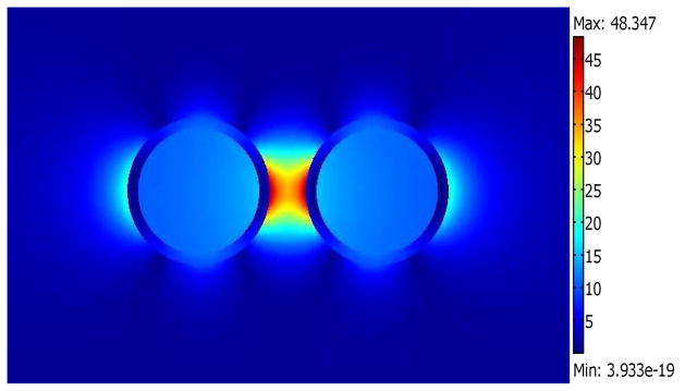
Electric-field magnitude of a 2-D x-z slice through the dimer with 15% shell thickness at a wavelength of 640 nm.
Figure 4.
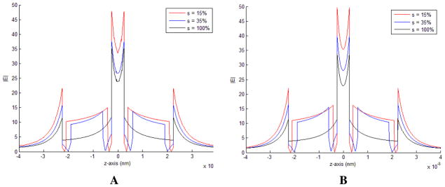
The magnitude of the electric field is shown here along the axis through the three dimer types: (A) FEM calculation using Comsol. (B) ME calculation.
The results in Figure 2 demonstrate that the agreement between the Comsol and ME calculations is within 5% across all geometries with respect to amplitude, wavelength offset and plasmon resonance FWHM. Figure 3 shows that Comsol employs tetrahedral meshes to accurately mesh around geometrical contours such that the fields are properly solved at curved boundaries. This is further emphasized in Figure 4, where the spatial line profiles, taken along the z-axis which cuts the geometry along its center, are in very good agreement between the two methods; the sharp discontinuities at the metal/dielectric boundaries are well resolved and the field amplitudes are also close in value.
3.2. Wafer-Scale plasmonic substrates for SERS sensing application
In parallel with our activities in theoretical and simulation studies of the EM enhancement, our investigations have been also devoted to designing and fabricating practical plasmonics-active substrates that can be used in microchip platforms for biosensing applications. Efforts by several researchers are currently devoted to maximizing the SERS signals emanating from molecules located or near the nanoscale gaps between plasmonically active metallic nanostructures on the SERS substrates.66–69 Some of the fabrication methods described in literature to develop plasmonics-active nanostructures include E-Beam Lithography,70 Deep UV Lithography, FIB milling,22 and nanosphere lithography.71 An earlier work in our laboratory has involved the development of planar solid substrates covered with a monolayer of nanospheres that are coated with a thin layer of silver, thus producing a plasmonics-active 2D half-nanoshell arrays.10, 72 It has not been practical to reproduce these SERS substrates over a large-area such as an entire wafer. Recent work to develop nanostructures on a large area plasmonic substrate includes development of nanowells73 using soft lithography and of nanoprism arrays69 using nanoimprint lithography (NIL). Although SERS substrates based on disordered metallic nanowires,74 and metal-coated silicon or germanium oxide nanowires75–76 have been described in the past literature, the ability to reproducibly develop ordered metallic nanowires with controlled sizes, shapes, and sub-10 nm gaps between the nanowires has not been presented previously.
Some of the challenges in developing novel SERS substrates lie in not only achieving large SERS enhancement factors but in also developing the substrates in a reliable and repeatable manner. One of the objectives of our research was to fabricate SERS active substrates on a wafer scale in a reproducible manner such that these substrates could be employed for detecting chemical and biological molecules. We fabricated highly efficient plasmonics-active one-dimensional (1D) nanowires, on an entire 6-inch wafer, for achieving a substantial electromagnetic enhancement in the SERS signals. Moreover, we were able to fabricate sub-10 nm nano-scale gap regions in these SERS substrates over the entire 6-inch wafer.
Wafer-Scale fabrication of plasmonic nanowire substrates
In the fabrication of the SERS-active substrates in a reproducible manner on a wafer scale, the first step involved the development of silicon nanowires (of varying sizes and spacings between the wires) on a 6- inch wafer. This was carried out using deep lithography and chemical etching to form silicon nanowires over the entire 6-inch wafer (See Figure 5A). The second step involved Atomic layer deposition (ALD) of a hafnium oxide spacer layer so that the gap between the nanowires and the width of the nanowires could be reduced in a reproducible manner (See Figure 5B). The wafer-scale SERS substrates (See Figure 6A) were developed by over-coating the nanowires (with or without the ALD conformal over layer) with thin film (10–100 nm) gold or silver. Electron beam evaporation was employed to deposit gold or silver films on the silicon nanowire substrates. As E-beam evaporation involves directional deposition of the metal films, the silicon nanowire substrates were placed right on top of the metal crucible (5–6 inches above) and the sample mount holding the substrates was rotated during the deposition process to improve uniformity as well as to obtain better coverage of the sidewalls of the underlying structure by the evaporated metal. Development of nanowires of different sizes and spacings allowed tunability of plasmon resonances of the gold-coated nanowires to different wavelengths. The gold nanowire structures shown in Figure 5B have deep grooves and sharp inverted triangular gap regions with sub-10nm gaps between the gold film regions. Tan et al.77 and Garcia Vidal et al.78 have previously explained the phenomenon of coupling of p-polarized incident radiation to surface plasmon polariton (SPP) modes in short-pitch, deep-groove metallic gratings thereby leading to enhancement in electromagnetic fields in the narrow between the metallic gratings.
Figure 5.
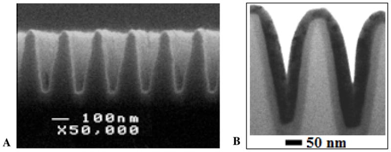
(A) SEM cross-section showing fabrication of a one-dimensional array of triangle-shaped silicon nanowires. The fabrication of silicon nanowires involved deep UV lithography followed by TMAH chemical etching of silicon. (B) TEM cross-section of a gold-coated silicon nanowire SERS substrate: Silicon nanowires (in light grey color) were over-coated with a conformal hafnium oxide layer (in dark grey color) to bridge the gap between the adjacent silicon nanowires in a controlled manner. Finally, a thin layer of gold film (in black color) was evaporated on the hafnium oxide layer to form inverted triangular structures, with sub-10 nm gaps between the metal surfaces.
Figure 6.
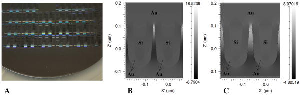
(A) Picture showing part of a 6 inch wafer-based SERS substrate having gold-coated silicon nanowire structures fabricated across the wafer. (B) FDTD calculations - carried out at 633 nm incident radiation wavelength - showing enhancement of the electric field in the gap between neighboring gold-coated silicon nanowires when the gap at the bottom of neighboring gold-coated silicon nanowires is 5 nm. (C) FDTD calculations as in (B) when the gap at the bottom of neighboring nanowires is 10 nm.
Modeling of EM Fields in the nanowire substrates
We performed 2-D Finite Difference Time Domain (FDTD) simulations to calculate electric field enhancement (and estimate the SERS EM enhancement, which is proportional to the fourth power of the E-Field enhancement) in the spacing between the nanowire structures (See Figures 6B and 6C). The FDTD software uses the Lorentz-Drude dispersion51–52, 79 model described above in Section 3.1. In the FDTD calculations, a continuous plane wave (633-nm for simulating the laser employed for SERS measurements) propagating in the z direction and having the electric field (E-field) polarized in the x direction was incident on the gold-coated silicon nanowire structures. Enhancement in E-field as a function of the incident field (normalized to 1) was calculated. The FDTD calculations indicate an increase in the electric field intensity, and therefore an increase in the SERS EM enhancement factor, as the spacing between the neighboring gold-coated silicon nanowires is decreased (See Figures 6B and 6C).
Sensing application using nanowire SERS substrates
To study the effect of nanowire spacing on SERS signals, the gold-coated nanowire SERS substrates were coated with a SERS-active dye, p-mercaptobenzoic acid (pMBA). Figure 7A shows SERS signals obtained from 1-mM p-mercaptobenzoic acid (pMBA) attached to the SERS substrates shown in Figure 5B. The SERS spectra of pMBA molecules show strong Raman bands at 1590 cm−1 and 1080 cm−1 corresponding to the ν8a and ν12 aromatic ring vibrations, respectively. One can observe in Figure 7A that the SERS signals at both 1590 cm−1 and 1080 cm−1 increase with decrease in the spacing between the nearest ends of nanowire structures shown in Figure 5B (this spacing between neighboring nanowires was measured at a region 50 nm above the bottom of the inverted triangular section of the gold-coated silicon nanowires). The increase in molecular signals on decreasing the spacing between the gold-coated silicon nanowires can be related to both an increase in the surface area of the nanowires as well as stronger plasmonic enhancement with smaller gap dimensions. It is seen in Figure 7A that as the spacing is decreased from 40 nm to 15 nm, intensity of the 1590 cm−1 SERS peak increases from 17000 to ~ 38000 photon counts. Increase in the SERS signal with an increase in spacing between the nanowires correlates well with FDTD calculations shown in Figures 6B and 6C which show an increase in the electric field enhancement, and therefore an increase in the SERS EM enhancement factor (which is known to be proportional to the fourth power of the electric field enhancement36), as the spacing between the neighboring gold-coated silicon nanowires is decreased. It can be seen that the SERS signal obtained from the gold pad region with no nanowires does not exhibit these Raman bands. We carried out SERS measurements to compare the SERS enhancement of the nanowire chip substrates with that of a gold film and found this enhancement factor to be in the 106–107 range.
Figure 7.
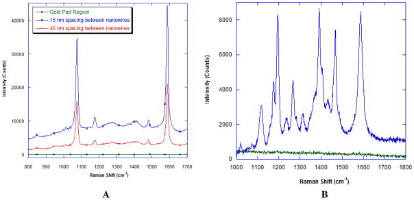
(A) SERS signals from pMBA molecules on gold-coated silicon nanowire substrates, for different spacing between neighboring nanowires in the one-dimensional array of nanowires. The SERS substrate chips were coated with pMBA molecules by dipping the chips in a 1 mM ethanol solution of pMBA. (B) SERS signal from Cy3 dye-labeled breast cancer gene sequence (ERBB2) molecules on gold-coated silicon nanowire substrates.
To illustrate the use of the nanowire substrates for biomedical sensing applications, we have used these substrates for SERS detection of a Raman-labeled gene probe as the sample system. The erbB-2 gene (also know as ERBB2 or HER2/neu), well known as a critical biomarker for breast cancer, encodes a transmembrane glycoprotein, which belongs to the epidermal growth factor receptor (EGFR) family and possesses intrinsic tyrosine kinase activity. Over-expression of ERBB2 is observed in 20% to 30% of invasive breast cancers.80,81 To detect labeled breast cancer DNA molecules, the gold-coated nanowire SERS substrates were dipped in a solution of a Cy3 dye-labeled ERBB2 gene sequence segment (5′ dithiol-AAA AAA AAA AGT CCG TC-cy3). Figure 7B shows SERS signal from labeled breast cancer DNA molecules (ERBB2), having SERS active dye Cy3 at the end of the DNA molecule, on a gold nanowire sample described by Figure 5B. Characteristic Raman peaks for the Cy3-labeled DNA molecules were observed at 1588 cm−1, 1469 cm−1, 1393 cm−1, and 1270 cm−1. The results indicate the potential of the nanochip structures for biomedical sensing applications.
4. Conclusion
The results of this study, both theoretically and experimentally, further indicate that the EM field enhancement is particularly strong in the interstitial spaces between nanoparticles and nanostructures. For sensing applications, this enhancement feature can be exploited effectively in the use of plasmonics-active systems consisting of densely packed nanoparticle aggregates and in the design of solid substrates having arrays of closely spaced nanostructures. Using advanced nanofabrication techniques, chip substrates having well controlled high-density nanostructures such as nanowires can be fabricated to produce sensitive and efficient chemical and biological sensing systems.
Acknowledgments
This work was sponsored by the National Institutes of Health (Grants R01 EB006201 and R01 ES014774-01A1) and Army Research Office (Grant No. W911NF-04-D-0001-0008).
Contributor Information
Tuan Vo-Dinh, Email: tuan.vodinh@duke.edu.
Anuj Dhawan, Email: anuj.dhawan@duke.edu.
Stephen J. Norton, Email: snorton@nc.rr.com.
Christopher G. Khoury, Email: christopher.khoury@duke.edu.
Hsin-Neng Wang, Email: hsinneng.wang@duke.edu.
Veena Misra, Email: vmisra@ncsu.edu.
Michael D. Gerhold, Email: michael.gerhold@us.army.mil.
References and Notes
- 1.Fleischmann, Hendra PJ, McQuillan AJ. Chem Phys Lett. 1974;26(2):163–166. [Google Scholar]
- 2.Jeanmaire DL, Vanduyne RP. J Electroanal Chem. 1977;84(1):1–20. [Google Scholar]
- 3.Albrecht MG, Creighton JA. J Am Chem Soc. 1977;99(15):5215–5217. [Google Scholar]
- 4.Moskovits M. Rev Modern Phys. 1985;57(3):783–826. [Google Scholar]
- 5.Wokaun A, Gordon JP, Liao PF. Phys Rev Lett. 1982;48(14):957–960. [Google Scholar]
- 6.Schatz GC. Acc Chem Res. 1984;17(10):370–376. [Google Scholar]
- 7.Kerker M. Acc Chem Res. 1984;17(8):271–277. [Google Scholar]
- 8.Chang RK, Furtak TE, editors. Surface Enhanced Raman Scattering. Plenum Press; New York: 1982. [Google Scholar]
- 9.Enhanced Raman Vibrational Studies at Solid/Gas Interfaces. Springer; Berlin: 1984. Pockrand, I. Surface. [Google Scholar]
- 10.Vo-Dinh T, Hiromoto MYK, Begun GM, Moody RL. Anal Chem. 1984;56(9):1667–1670. [Google Scholar]
- 11.Enlow PD, Buncick M, Warmack RJ, Vo-Dinh T. Anal Chem. 1986;58:1719–1724. [Google Scholar]
- 12.Vo-Dinh T, Uziel M, Morrison AL. Appl Spectrosc. 1987;41(4):605–610. [Google Scholar]
- 13.Moody RL, Vo-Dinh T, Fletcher WH. Appl Spectrosc. 1987;41(6):966–970. [Google Scholar]
- 14.Alak AM, Vo-Dinh T. Anal Chem. 1987;59(17):2149–2153. doi: 10.1021/ac00144a030. [DOI] [PubMed] [Google Scholar]
- 15.Vo-Dinh T, Alak A, Moody RL. Spectrochim Acta, Part B. 1988;43(4–5):605–615. [Google Scholar]
- 16.Bello JM, Stokes DL, Vo-Dinh T. Appl Spectrosc. 1989;43(8):1325–1330. [Google Scholar]
- 17.Bello JM, Stokes DL, Vo-Dinh T. Anal Chem. 1989;61(15):1779–1783. [Google Scholar]
- 18.Vo-Dinh T, Houck K, Stokes DL. Anal Chem. 1994;66(20):3379–3383. doi: 10.1021/ac00092a014. [DOI] [PubMed] [Google Scholar]
- 19.Vo-Dinh T. Trac-Trends Anal Chem. 1998;17(8–9):557–582. [Google Scholar]
- 20.Isola NR, Stokes DL, Vo-Dinh T. Anal Chem. 1998;70(7):1352–1356. doi: 10.1021/ac970901z. [DOI] [PubMed] [Google Scholar]
- 21.Zeisel D, Deckert V, Zenobi R, Vo-Dinh T. Chem Phys Lett. 1998;283(5–6):381–385. [Google Scholar]
- 22.Dhawan A, Muth JF, Leonard DN, Gerhold MD, Gleeson J, Vo-Dinh T, Russell PE. J Vac Sci Technol. 2008;26:2168–2173. doi: 10.1116/1.3013329. [DOI] [PMC free article] [PubMed] [Google Scholar]
- 23.Khoury CG, Vo-Dinh T. J Phys Chem C. 2008;112(48):18849–18859. doi: 10.1021/jp8054747. [DOI] [PMC free article] [PubMed] [Google Scholar]
- 24.Stokes DL, Chi ZH, Vo-Dinh T. Appl Spectroscopy. 2004;58(3):292–298. doi: 10.1366/000370204322886636. [DOI] [PubMed] [Google Scholar]
- 25.Vo-Dinh T, Allain LR, Stokes DL. J Raman Spectrosc. 2002;33(7):511–516. [Google Scholar]
- 26.Vo-Dinh T, Yan F, Wabuyele MB. J Raman Spectrosc. 2005;36(6–7):640–647. [Google Scholar]
- 27.Wabuyele MB, Yan F, Griffin GD, Vo-Dinh T. Rev Sci Instrum. 2005;76(6):063710-1–063710-7. [Google Scholar]
- 28.Wabuyele MB, Vo-Dinh T. Anal Chem. 77(23):7810–7815. doi: 10.1021/ac0514671. 005. [DOI] [PubMed] [Google Scholar]
- 29.Vo-Dinh T, Yan F. Gene Detection and Multi-spectral Imaging Using SERS Nanoprobes and Nanostructures. In: Vo-Dinh T, editor. Nanotechnology in Biology and Medicine. Taylor and Francis Publishers; New York: 2007. [Google Scholar]
- 30.Wang HN, Vo-Dinh T. Nanotechnology. 2009;20(6):065101-1–065101-6. doi: 10.1088/0957-4484/20/6/065101. [DOI] [PMC free article] [PubMed] [Google Scholar]
- 31.Scaffidi JP, Gregas MK, Seewaldt V, Vo-Dinh T. Anal Bioanal Chem. 2009;393(4):1135–1141. doi: 10.1007/s00216-008-2521-y. [DOI] [PMC free article] [PubMed] [Google Scholar]
- 32.Moskovits M. Rev Mod Phys. 1985;57(3):783–826. [Google Scholar]
- 33.Moskovits M. J Raman Spectrosc. 2005;36(6–7):485–496. [Google Scholar]
- 34.Doering WE, Nie SM. J Phys Chem B. 2002;106(2):311–317. [Google Scholar]
- 35.Cao YWC, Jin RC, Mirkin CA. Science. 2002;297(5586):1536–1540. doi: 10.1126/science.297.5586.1536. [DOI] [PubMed] [Google Scholar]
- 36.Otto A, Mrozek I, Grabhorn H, Akemann W. J Phys: Condens Matter. 1992;4(5):1143–1212. [Google Scholar]
- 37.Kneipp K, Moskovits M, Kneipp H, editors. Surface-enhanced Raman Scattering: Physics and Applications. Springer; New York: 2006. [Google Scholar]
- 38.Xu HX, Aizpurua J, Kall M, Apell P. Phys Rev E. 2000;62(3):4318–4324. doi: 10.1103/physreve.62.4318. [DOI] [PubMed] [Google Scholar]
- 39.Kneipp K, Wang Y, Kneipp H, Perelman LT, Itzkan I, Dasari R, Feld MS. Phys Rev Lett. 1997;78(9):1667–1670. [Google Scholar]
- 40.Xu HX, Bjerneld EJ, Kall M, Borjesson L. Phys Rev Lett. 1999;83(21):4357–4360. [Google Scholar]
- 41.Nie SM, Emery SR. Science. 1997;275(5303):1102–1106. doi: 10.1126/science.275.5303.1102. [DOI] [PubMed] [Google Scholar]
- 42.Michaels AM, Jiang J, Brus L. J Phys Chem B. 2000;104(50):11965–11971. [Google Scholar]
- 43.Garcia-Vidal FJ, Pendry JB. Phys Rev Lett. 1996;77(6):1163–1166. doi: 10.1103/PhysRevLett.77.1163. [DOI] [PubMed] [Google Scholar]
- 44.Aravind PK, Metiu H. Chem Phys Lett. 1980;74(2):301–305. [Google Scholar]
- 45.Norton SJ, Vo-Dinh T. J Opt Soc Am A. 2008;25(11):2767–2775. doi: 10.1364/josaa.25.002767. [DOI] [PMC free article] [PubMed] [Google Scholar]
- 46.Oubre C, Nordlander P. J Phys Chem B. 2005;109(20):10042–10051. doi: 10.1021/jp044382x. [DOI] [PubMed] [Google Scholar]
- 47.Brandl DW, Oubre C, Nordlander P. J Chem Phys. 2005;123(2):024701-1–024701-11. doi: 10.1063/1.1949169. [DOI] [PubMed] [Google Scholar]
- 48.Nordlander P, Oubre C, Prodan E, Li K, Stockman MI. Nano Lett. 2004;4(5):899–903. [Google Scholar]
- 49.Pellegrini G, Mattei G, Bello V, Mazzoldi P. Mat Sci & Eng C. 2007;27:1347–1350. [Google Scholar]
- 50.Lassiter JB, Aizpurua J, Hernandez LI, Brandl DW, Romero I, Lal S, Hafner JH, Nordlander P, Halas NJ. Nano Lett. 2008;8(4):1212–1218. doi: 10.1021/nl080271o. [DOI] [PubMed] [Google Scholar]
- 51.Dhawan A, Norton SJ, Gerhold MD, Vo-Dinh T. Opt Express. 2009;17:9688–9703. doi: 10.1364/oe.17.009688. [DOI] [PubMed] [Google Scholar]
- 52.Khoury CG, Norton SJ, Vo-Dinh T. ACS Nano. 2009;3(9):2776–2788. doi: 10.1021/nn900664j. [DOI] [PMC free article] [PubMed] [Google Scholar]
- 53.Gerardy JM, Ausloos M. Phys Rev B. 1980;22:4950–4959. [Google Scholar]
- 54.Kneipp K, Kneipp H, Manoharan R, Hanlon EB, Itzkan I, Dasari RR, Feld MS. Appl Spectrosc. 1998;52(12):1493–1497. [Google Scholar]
- 55.Quinten M, Leitner A, Krenn JR, Aussenegg FR. Opt Lett. 1998;23(17):1331–1333. doi: 10.1364/ol.23.001331. [DOI] [PubMed] [Google Scholar]
- 56.Li KR, Stockman MI, Bergman DJ. Phys Rev Lett. 2003;91(22):227402-1–227402-4. doi: 10.1103/PhysRevLett.91.227402. [DOI] [PubMed] [Google Scholar]
- 57.Zou SL, Schatz GC. Chem Phys Lett. 2005;403:62–67. [Google Scholar]
- 58.Sweatlock LA, Maier SA, Atwater HA, Penninkhof JJ, Polman A. Phys Rev B. 2005;71(23):235408-1–235408-7. [Google Scholar]
- 59.Cui X, Erni D. J Opt Soc Am A. 2008;25:1783–1789. doi: 10.1364/josaa.25.001783. [DOI] [PubMed] [Google Scholar]
- 60.Hirsch LR, Stafford RJ, Bankson JA, Sershen SR, Rivera B, Price RE, Hazle JD, Halas NJ, West JL. Proc Natl Acad Sci U S A. 2003;100(23):13549–13554. doi: 10.1073/pnas.2232479100. [DOI] [PMC free article] [PubMed] [Google Scholar]
- 61.Jackson JB, Westcott SL, Hirsch LR, West JL, Halas NH. Appl Phys Lett. 2003;82:257–259. [Google Scholar]
- 62.El-Sayed IH, Huang X, El-Sayed MA. Cancer Lett. 2006;239(1):129–135. doi: 10.1016/j.canlet.2005.07.035. [DOI] [PubMed] [Google Scholar]
- 63.Caola MJ. J Phys A. 1978;11:L23–L25. [Google Scholar]
- 64.Palik ED, editor. Handbook of Optical Constants of Solids. Academic Press; San Diego: 1998. [Google Scholar]
- 65.Moroz A. J Phys Chem C. 2008;112:10641–10652. [Google Scholar]
- 66.Qin LD, Zou SL, Xue C, Atkinson A, Schatz GC, Mirkin CA. Proc Natl Acad Sci U S A. 2006;103(36):13300–13303. doi: 10.1073/pnas.0605889103. [DOI] [PMC free article] [PubMed] [Google Scholar]
- 67.Schierhorn M, Lee SJ, Boettcher SW, Stucky GD, Moskovits M. Adv Mater. 2006;18(21):2829–2832. [Google Scholar]
- 68.Zhao LL, Jensen L, Schatz GC. Nano Lett. 2006;6(6):1229–1234. doi: 10.1021/nl0607378. [DOI] [PubMed] [Google Scholar]
- 69.Cui B, Clime L, Li K, Veres T. Nanotechnology. 2008;19(14):145302-1–145302-6. doi: 10.1088/0957-4484/19/14/145302. [DOI] [PubMed] [Google Scholar]
- 70.Felidj N, Aubard J, Levi G, Krenn JR, Hohenau A, Schider G, Leitner A, Aussenegg FR. Appl Phys Lett. 2003;82(18):3095–3097. [Google Scholar]
- 71.Dieringer JA, McFarland AD, Shah NC, Stuart DA, Whitney AV, Yonzon CR, Young MA, Zhang XY, Van Duyne RP. Faraday Discuss. 2006;132:9–26. doi: 10.1039/b513431p. [DOI] [PubMed] [Google Scholar]
- 72.Zhang XY, Young MA, Lyandres O, Van Duyne RP. J Am Chem Soc. 2005;127(12):4484–4489. doi: 10.1021/ja043623b. [DOI] [PubMed] [Google Scholar]
- 73.Liu GL, Lee LP. Appl Phys Lett. 2005;87(7):074101-1–074101-3. [Google Scholar]
- 74.Lee SJ, Morrill AR, Moskovits M. J Am Chem Soc. 2006;128(7):2200–2201. doi: 10.1021/ja0578350. [DOI] [PubMed] [Google Scholar]
- 75.Qiu T, Wu XL, Shen JC, Ha PCT, Chu PK. Nanotechnology. 2006;17(23):5769–5772. [Google Scholar]
- 76.Khan MA, Hogan TP, Shanker B. J Raman Spectrosc. 2008;39(7):893–900. [Google Scholar]
- 77.Tan WC, Preist TW, Sambles JR, Wanstall NP. Phys Rev B. 1999;59(19):12661–12666. [Google Scholar]
- 78.Garcia-Vidal FJ, Martin-Moreno L. Phys Rev B. 2002;66(15):155412-1–155412-10. [Google Scholar]
- 79.Dhawan A, Gerhold MD, Vo-Dinh T. Nanobiotechnology. 2007;3:1–8. doi: 10.1007/s12030-008-9017-x. [DOI] [PMC free article] [PubMed] [Google Scholar]
- 80.Menard S, Tagliabue E, Campiglio M, Pupa SM. J Cell Physiol. 2000;182:150–162. doi: 10.1002/(SICI)1097-4652(200002)182:2<150::AID-JCP3>3.0.CO;2-E. [DOI] [PubMed] [Google Scholar]
- 81.Slamon DJ, Clark GM, Wong SG, Levin WJ, Ullrich A, McGuire WL. Science. 1987;235:177–182. doi: 10.1126/science.3798106. [DOI] [PubMed] [Google Scholar]