Abstract
Based on the extensive application of 2 × 1.7MV Tandetron accelerator, a low-energy cluster chamber has been built to explore for synthesizing graphene. Raman spectrum and atomic force microscopy (AFM) show that an amorphous carbon film in nanometer was deposited on the silicon by C4 cluster implantation. And we replaced the substrate with Ni/SiO2/Si and measured the thickness of Ni film by Rutherford backscattering spectrometry (RBS). Combined with suitable anneal conditions, these samples implanted by various small carbon clusters were made to grow graphene. Results from Raman spectrum reveal that few-layer graphene were obtained and discuss whether IG/I2D can contribute to explain the relationship between the number of graphene layers and cluster implantation dosage.
Keywords: Carbon cluster, Low-energy implantation, Graphene, Raman spectra
Keywords: 29.20.-c, 29.25.Ni, 81.05.-t
Background
In the past of several decades, ion beam analysis (IBA) based on low-energy accelerator has developed to be a comprehensive particle analytical discipline system [1-4]. A further exploitation of what can be paid more attention has springed up on the functional materials [5], in situ observation for defects on semiconductor industry and the simulation of multi-ion irradiation environment. For instance, the energetic ion-solid interaction was taken as a classic model to characterize some structure information of superconductor at room temperature or high K by projecting MeV ions to impact on superconductive targets [6]. In order to understand the influence induced by implanting multi-energy ions to the substrate, in particular several defects that lead to some phase transitions in matter, in situ characterization of these transients which can exhibit a clear physical image on changeable process of the structure was performed by the accelerator-transmission electron microscopy (TEM) interface system [7,8]. For practical application of multi-particle irradiation, the purpose of fabricating the multi-ion irradiation stage associated with simulation of the realistic environment where some special materials or functional devices are used is scientific and effective [9,10]. In a way, not only can ion beam analysis take full advantage of probing the stoichiometry but can also trace reasonable explanation on structure details of the matter [11].
In Wuhan University, the double 1.7 MV Tandetron accelerator was inherited from Physical Institution of Chinese Academy of Sciences in 2004. After several important maintenances and upgrades of facility, some primary ion beam analysis with terminal voltage at 1.2 MV can be performed in a good state, such as Rutherford backscattering spectrometry (RBS), elastic recoil detection analysis (ERDA), and nuclear reaction analysis (NRA). Besides, we have developed some extensive applications, including accelerator-TEM interface system [7] and double-ion beam radiation chamber and another new design of low-energy cluster chamber for ion implantation.
As another kind of ultra-thin carbon film, graphene is a promising material which is probable to replace silicon integration technique due to its advanced and novel physical properties [12,13]. But a key issue for preparing larger scale and continuous thin film is always not comprehensively figured out. Garaj et al. and Baraton et al. have reported graphene synthesis by ion implantation at 30 keV [14] and 80 keV [15], respectively. But cluster ions have not been involved, especially in the case of lower energy implantation. Therefore, it is a reasonable attempt that can be attributed to much shallower penetration depth from low-energy cluster ions to dedicate to carbon atoms precipitation form the transition metal under subsequent thermal treatments. In this work, above low-energy cluster chamber is addressed to synthesis nanostructure carbon materials including ultra-thin film and graphene, expanding fundamental ion beam applications in this machine.
Methods
Low-energy cluster chamber
A source of negative ion by cesium sputtering (SNICS) can produce various negative ions from solid targets, such as B−, C−, Si−, P−, Fe−, Cu−, and Au−[16,17], which can be implanted into the substrates after being accelerated up to the maximum 30 keV depending on the accelerator field. Selecting cluster ions with small size as projectiles to perform the process of low-energy ion implantation can form shallow layer architectures in the matrix, which is beneficial to fabricate ultra-shallow junction devices.
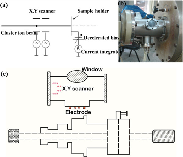
Figure 1a,b illustrates the schematic diagram of low-energy cluster deposition. In our previous study [18], some carbon cluster ions (Cn−) from SNICS at an energy of 20 keV are chosen for desirable targets by mass analyzer, then are decelerated to a few hundred electron volt or below 3 keV by the deceleration field after voltage scanner mounted on two aligned directions of X and Y-axis, finally to soft-land to the substrate. The current integrator is used for monitoring implantation dose simultaneously. To eliminate some impacts on the current integrator from high voltage at decelerated filed, an isolation transformer was introduced to guarantee safety. In addition, a rotated target holder (Figure 1c) was designed to change projectile ranges of cluster ions by regulating the angle between incident ion and the substrate. The overall layout, similar to ion beam-assisted deposition, was executed to deposit carbon cluster ions onto the surface of silicon for graphene synthesis. Unfortunately, it is not successful to obtain graphene for this method. However, some ultra-thin carbon films on the silicon were prepared with the scale of several nanometers.
Figure 1.
Schematic diagram of low-energy cluster deposition. (a) The schematic diagram of cluster ion deposition. (b) The graph of deposition in chamber. (c) Top view of chamber and the rotated sample holder.
Results and discussion
Ultra-thin carbon film deposition
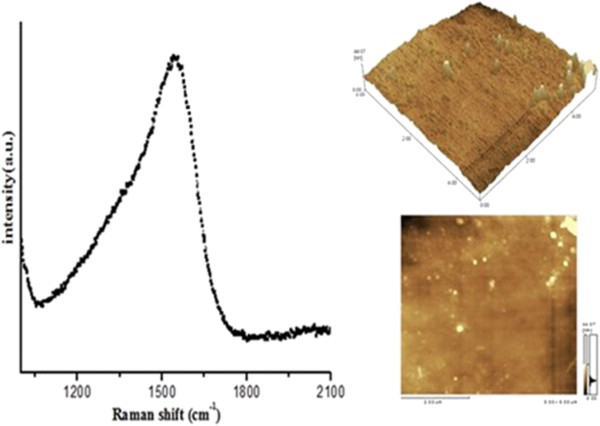
Figure 2 shows Raman spectrum and atomic force microscopy (AFM) images of the sample synthesized by C4 ions implantation. The projectile range of C4 in the silicon is approximately 5 nm at 14 keV, which was calculated by SRIM 2008 edition [19]. About 12 kV terminal voltages were reversed to slow down the kinetic energy of cluster ions so as to soft-land onto the surface of the sample. Expectedly, such low-energy interactions of cluster target can lead to little cascade collisions. Raman spectra indicate that there is an amorphous carbon film on the sample due to sp2 hybridized carbon atoms forming π-bond to enhance Raman scattering cross section, which is performing drastic peak intensities at about 1,560 cm−1. In conjunction with the surface morphology of AFM image, the amorphous layer exhibits continuous distributions on the whole substrate except some possible island-like contaminations in the form of white spots. Certainly, these columnar protuberances may be some larger grain accumulations induced by higher energetic ions landing on the edge than that in the center of the sample, depending on the strength distribution of decelerated field. The value of root mean square roughness (RMS) is about 5.10 nm for thin film, which indicates a great promise of preparing ultra-thin film under much lower energy ion implantation.
Figure 2.
Raman spectra and AFM image of the sample by C 4 cluster ion implantation.
Few-layer graphene synthesis
It is an essential purpose that we designed this low-energy cluster chamber for graphene preparation. In the process of exploring some effective methods, after depositing carbon films with the scale of several nanometers on the silicon, we selected suitable substrates to succeed in achieving few-layer graphene. Uninstalling the decelerated field, we selected small carbon cluster ions to inject to the substrate below 30 keV. The substrate Ni/SiO2/Si with about 300 nm Ni film deposited Ni atoms onto silica by e-beam evaporating.
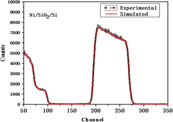
The thickness of Ni film has influence on carbon segregation from inside up to the surface, so it is significant to evaluate the thickness of the substrate, and RBS spectra of the sample was carried out, as shown in Figure 3. Incident 2.86 MeV Li2+ which was produced by the double 1.7 MV tandem accelerator was collimated to the target with ion current of 5 nA and the round beam spot of 1.5 mm. The backscattered ions were detected by passivated implanted planar silicon (PIPS) detector with the resolution of 14 keV for α particle at 165°. The abscissa of spectra stands for channel numbers of multi-channel analyzer (MCA), which is proportional to the energy of scattered ions. A broad peak indicates that the surface edge of Ni is about channel 269 and the back edge is about channel 195. The channel difference of both edges is corresponding to the energy loss of projectile Li ions in Ni in correlation with the thickness of thin film. A straightforward route is simulating the trajectories of incident ions in matter. The red curve of this graph is simulation result from SIMNRA6.05 code, which is in coincidence with experimental data absolutely. The simulated results reveal that the areal density of Ni film is 2.1 × 10¹⁸ atoms/cm2, and a corresponding thickness is 227.3 nm in the case of the volume density at 8.9 g/cm3, which is thinner than the estimated value.
Figure 3.
RBS spectra of Ni/SiO2/Si with incident 2.86 MeV Li 2+ .
With regard to depositing Ni film onto silica but not silicon substrate, it was reported that the silicon oxide at a thickness of 300 nm can enhance scattered signals of Raman resonance spectrum drastically because photon can evoke continuous interferences at the interface between Ni and silica [20]. All the matrixes were implanted with the same dosage at 8 × 1015 cm−2 by ion implantation consisting of different cluster sizes at 20 keV. After implantation, these samples were annealed from room temperature to 900°C and dwell time was 60 min, then cooled down to room temperature naturally at 2.0 torr.
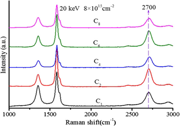
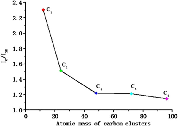
Raman spectroscopy is always employed as one of the powerful non-destructive methods to identify graphene and determine the layer of graphene [15,21]. In this study, Raman scattering was excited by an Ar laser at 514 nm and the power at the sample is below 1 mW for avoiding radiation damage. Figure 4 shows Raman spectra of the samples. For 514-nm wavelength laser, D peak position at 1,350 cm−1 is relative to the disorder and defects in the structures performing sp3 hybridization of carbon atoms, while sp2 hybridization induced by the in-plan optical phonon E2g near the first Brillouin Zone center is characterized as G peak at 1,580 cm−1[22]. The 2D peak position at 2,700 cm−1 of graphene is single and symmetrical to characterize monolayer. These samples were implanted with the same dosage of 8 × 10¹⁵ carbon atoms/cm2 at 20 keV by the different small carbon cluster sizes (C1, C2, C4, C6, C8). Almost the three characteristic peak positions appear, and every peak position for different cluster sizes has also negligible shifts, as shown in Figure 4. In most literatures, 2D peak position at 2,700 cm−1 and IG/I2D (the intensity ratio of G peak and 2D peak), which is the smaller and thinner film that can be obtained, were also evaluated to differentiate graphite and confirm the layers of graphene sheets [20]. The range of 2D peak position is 2,704 to 2,709 cm−1 in the spectra, corresponding to three and more layers. A visualized trend is observed that IG/I2D decreases as carbon cluster size increases, described in Figure 5. There is a drastic decline for small clusters C1 to C4, meanwhile larger clusters C4, C6, C8 are presenting a relatively gradual shrink. In the case of such low-energy ion implantation, light cluster can penetrate into deeper sites than heavy cluster in the substrate, which is dependent on the energy distribution of cascade collision between cluster and matter.
Figure 4.
Raman spectra of the samples implanted by the different kinds of carbon clusters Cn(n = 1, 2, 4, 6, 8).
Figure 5.
The intensity ratio I G / I 2D as functions of the mass small carbon cluster.
In previous studies, we have achieved some carbon cluster mass spectra at the different extractor voltages of sputtering ion source in this machine and paid much attention to investigate Raman characterizations of graphene by means of the carbon cluster ion implantation [18,23]. Because the cluster ion current can be influenced from cluster size and extractor bias strongly, selecting small carbon cluster ions to carry out implantation is out of more time consumptions. However, more defects can be produced by cluster C1 implantation instead of saving time. For example, implantation time is about 8.5 h for cluster C8 at 20 keV in this work, but the IG/I2D ratio is the smallest which indicates that the graphene quality is better than that in the other smaller cluster sizes.
Simply, E0 is cluster energy, and every atom of Cn cluster can be allocated as homogeneous energy of E0/n. Therefore, in comparison with C1, C n (n > 1) has more sophisticated interactions with the substrate, involving in non-linear damage effect and atomic self-sputtering effect [24,25]. During such low-energy shallow ion implantation, carbon atom contents in Ni film may reach up to saturation at certain implantation dosage, which is significant for cluster aggregation to interact with the substrate. Graphene nucleation on the transition metal has been investigated to a theoretical growth issue that strongly depends on segregation and precipitation on the grain boundaries of the substrate after thermal treatment [26], no matter how to prepare graphene, by chemical vapor deposition (CVD) or ion implantation [14,15,20,21]. Baraton et al. have proposed that the anneal temperature from 900°C to 725°C, half of the carbon atoms were removed to grain boundaries of Ni surface to form graphene; that is to say, 4 × 1015 cm−2 and 8 × 1015 cm−2 of carbon concentration on the surface are in agreement with monolayer and bilayer graphene [15], respectively. However, it is not successful to control the number of graphene layers accurately by regulating the contents of implantation carbon atoms. We always seek to graphene synthesis with fewer defects by low-energy cluster ion technique; larger cluster size C n (n > 10) under suitable energy is more likely to develop this process. But we have to take the atomic self-sputtering effect and more sophisticated cluster-matter interaction into consideration. More investigations are probable to promote the nucleation mechanism of graphene including ion-matter interaction, crystal quality of the substrate, anneal temperature, and other details about growth conditions.
Conclusions
We have developed a low-energy cluster chamber on the base of extensive application for the double 1.7 MV Tandetron accelerator, which was used to explore for graphene synthesis. In our previous work, a kind of amorphous ultra-thin carbon film was fabricated by projecting C4 cluster ions to the silicon at 14 keV, and the RMS is about 5.10 nm. Another substrates Ni/SiO2/Si whose thickness was measured at 227.3 nm by RBS were implanted with the same carbon atoms at 8 × 1015 cm−2 by several kinds of small clusters C n (n = 1, 2, 4, 6, 8); after annealing, Raman spectra indicate that few-layer graphene was prepared successfully. And the ratio IG/I2D shows that the number of graphene layers cannot be controlled by implantation dosage purely but are associated with carbon atoms precipitation and segregation from inside to the surface grain boundaries of the substrate during thermal treatment. From ultra-thin carbon film to graphene by means of the similar cluster ion implantation technique, it is conductive for cluster implantation of light elements to develop low-energy shallow ion implantation in semiconductor industry.
Abbreviations
AFM: atomic force microscopy; ERDA: elastic recoil detection analysis; IBA: ion beam analysis; MCA: multi-channel analyzer; NRA: nuclear reaction analysis; RBS: Rutherford backscattering spectrometry; RMS: root mean square roughness; TEM: transmission electron microscopy.
Competing interests
The authors declare that they have no competing interests.
Authors’ contributions
ZW designed parts of the experiments and sample preparations and drafted the manuscript. DF is the corresponding author and provided a great help for experimental designs. Other co-authors took part in sample preparation and characterizations and discussed the results. All authors have read and approved the final manuscript.
Contributor Information
Zesong Wang, Email: zs_wang055@whu.edu.cn.
Zaodi Zhang, Email: 872972242@qq.com.
Rui Zhang, Email: zrzx_0921@163.com.
Hui Li, Email: 528785058@qq.com.
Dejun Fu, Email: djfu@whu.edu.cn.
Acknowledgements
This work was supported by the National Natural Science Foundation of China under grant 11350110206 and the Fundamental Research Funds for the Central Universities under the contract (No. 201120202020005). And we sincerely appreciated for help from Professor Liu (jrliu@central.uh.edu) who proposed some constructive suggestions for experimental design.
References
- Mayer M. Ion beam analysis of rough thin films. Nucl Instrum Methods B. 2002;9:177. doi: 10.1016/S0168-583X(02)00689-4. [DOI] [Google Scholar]
- Barradas NP, Parascandola S, Sealy BJ, Grotzschel R, Kreissig U. Simultaneous and consistent analysis of NRA RBS and ERDA data with IBA Data Furnace. Nucl Instrum Methods B. 2000;9:308. [Google Scholar]
- Jeynes C, Barradas NP, Marriott PK, Boudreault G, Jenkin M, Wendler E, Webb RP. Elemental thin film depth profiles by ion beam analysis using simulated annealing-a new tool. J Phys D ApplPhys. 2003;9:97. [Google Scholar]
- Wang Y, Nastasi M. Handbook of modern ion beam materials analysis. 2. England: Cambridge University Press; 2010. [Google Scholar]
- Barradas NP, Almeida SA, Jeynes AC, Knights AP, Silva $RP, Sealy BJ. RBS and ERDA simulated annealing study of ion beam synthesized gallium nitride. Nucl Instrum Methods B. 1999;9:463. [Google Scholar]
- Chu WK, Li YP, Liu JR, Wu JZ, Tidrow SC, Toyoda N, Matsuo J, Yamada I. Smoothing of YB2Cu3O7-δfilms by ion cluster bombardment. Appl Phys Lett. 1998;9:246. doi: 10.1063/1.120699. [DOI] [Google Scholar]
- Song B, Guo LP, Li M, Liu CS, Ye MS, Fu DJ, Fan XJ. Accelerator-electron microscope interface system at Wuhan University. Nucl Techni. 2007;9(9):777. [Google Scholar]
- Guo LP, Li M, Liu CS, Song B, Fu DJ, Fan XJ. In situ TEM-tandem/implanter interface facility in Wuhan University for investigation of radiation effects. Guilin, China: ; 2007. (9thChina-Japan Symposium on Materials for Advanced Energy Systems and Fission & Fusion Engineering jointed with CAS-JSPS Core-university Program Seminar on Fusion Materials, System and Design Integration). [Google Scholar]
- Mukouda I, Shimomura Y, Yamaki D, Nakazawa T, Aruga T, Jitsukawa S. Microstructure in pure copper irradiated by simultaneous multi-ion beam of hydrogen, helium and self ions. J Nucl Mater. 2000;9:302. [Google Scholar]
- Appleton BR, Tongay S, Lemaitre M, Gial B, Fridmann J, Mazarov P, Sanabia JE, Bauerdick S, Bruchhaus L, Minura R, Jede R. Materials modifications using multi-ion processing and lithography system. Nucl Instrum Methods B. 2012;9:153. [Google Scholar]
- Cappellani A, Keddie JL, Barradas NP, Jackson SM. Processing and characterization of sol–gel deposited Ta2O5and TiO2-Ta2O5dielectric thin film. Solid-State Electron. 1999;9:1095. doi: 10.1016/S0038-1101(99)00031-3. [DOI] [Google Scholar]
- Ohta T, Bostwick A, Seyller T, Horn K, Rotenberg E. Controlling the electronic structure of bilayer graphene. Science. 2006;9:951. doi: 10.1126/science.1130681. [DOI] [PubMed] [Google Scholar]
- Oostinga JB, Heersche HB, Liu XL, Morpurgo AF, Vandersypen LMK. Gate-induced insulating state in bilayer graphene devices. Nat Mater. 2007;9:151. doi: 10.1038/nmat2082. [DOI] [PubMed] [Google Scholar]
- Garaj S, Hubbard W, Golovchenko JA. Graphene synthesis by ion implantation. ApplPhysLett. 2010;9:183103. doi: 10.1063/1.3507287. [DOI] [PMC free article] [PubMed] [Google Scholar]
- Baraton L, He ZB, Lee CS, Maurice JL, Cajocaru CS, Lorenzon A-F G, Lee YH, Pribat D. Synthesis of few-layered graphene by ion implantation of carbon in nickel thin films. Nanotechnology. 2011;9:085601. doi: 10.1088/0957-4484/22/8/085601. [DOI] [PubMed] [Google Scholar]
- Wang XM, Lu XM, Shao L, Liu JR, Chu WK. Small cluster ions from source of negative ions by cesium sputtering. Nucl Instrum Methods B. 2002;9:198. doi: 10.1016/S0168-583X(02)01302-2. [DOI] [Google Scholar]
- Liu JR, Wang XM, Shao L, Chen H, Chu WK. Small B-cluster ions induced damage in silicon. Nucl Instrum Methods B. 2005;9:636. [Google Scholar]
- Wang ZS, Zhang ZD, Zhang R, Wang SX, Fu DJ, Liu JR. An ultralow-energy negative cluster ion beam system and its application in preparation of few-layer graphene. Chin Sci Bull. 2012;9:3556. doi: 10.1007/s11434-012-5397-3. [DOI] [Google Scholar]
- Ziegler JF. Stimulated program by SRIM 2008 edition. http://www.srim.org.
- Ni ZH, Wang YY, Yu T, Shen ZX. Raman spectroscopy and imaging of graphene. Nano Res. 2008;9:273. doi: 10.1007/s12274-008-8036-1. [DOI] [Google Scholar]
- Wang G, Ding GQ, Zhu Y, Chen D, YE L, Zheng L, Zhang M, Di ZF, Liu S. Growth of controlled thickness graphene by ion implantation for field-effect transistor. Matter Lett. 2013;9:170. [Google Scholar]
- Ferrari AC, Basko DM. Raman spectroscopy as a versatile tool for studying the properties of graphene. Nat Nanotechnol. 2013;9:235. doi: 10.1038/nnano.2013.46. [DOI] [PubMed] [Google Scholar]
- Wang ZS, Zhang R, Zhang ZD, Huang ZH, Liu CS, Fu DJ, Liu JR. Raman spectroscopy of few-layer graphene prepared by C2-C6cluster ion implantation. Nucl Instrum Methods B. 2013;9:40. [Google Scholar]
- Jin JY, Liu JR, Paul AW, Chu WK. Implantation damage effect on boron annealing behavior using low-energy polyatomic ion implantation. Appl Phys Lett. 2000;9:574. doi: 10.1063/1.125821. [DOI] [Google Scholar]
- Zhang R, Zhang ZD, Wang ZS, Wang XU, Wang W, Fu DJ, Liu JR. Nonlinear damage effect in graphene synthesis by C-cluster ion implantation. Appl Phys Lett. 2012;9:011905. doi: 10.1063/1.4732088. [DOI] [Google Scholar]
- Baraton L, He ZB, Lee CS, Cojocaru CS, Chatelet M, Maurice JL, Lee YH, Pribat D. On the mechanisms of precipitation of graphene on nickel thin films. Euro Phys Lett. 2011;9:46003. doi: 10.1209/0295-5075/96/46003. [DOI] [Google Scholar]


