

Significance
A new class of heterostructures consisting of layered transition metal dichalcogenide components can be designed and built by van der Waals (vdW) stacking of individual monolayers into functional multilayer structures. Nonetheless, the optoelectronic properties of this new type of vdW heterostructure are unknown. Here, we investigate artificial semiconductor heterostructures built from single-layer WSe2 and MoS2. We observe spatially direct absorption but spatially indirect emission in this heterostructure, with strong interlayer coupling of charge carriers. The coupling at the hetero-interface can be readily tuned by inserting hexagonal BN dielectric layers into the vdW gap. The generic nature of this interlayer coupling is expected to yield a new family of semiconductor heterostructures having tunable optoelectronic properties through customized composite layers.
Keywords: MoS2-WSe2 heterostructure, Moiré pattern, charge transfer, exciton relaxation, rectifying
Abstract
Semiconductor heterostructures are the fundamental platform for many important device applications such as lasers, light-emitting diodes, solar cells, and high-electron-mobility transistors. Analogous to traditional heterostructures, layered transition metal dichalcogenide heterostructures can be designed and built by assembling individual single layers into functional multilayer structures, but in principle with atomically sharp interfaces, no interdiffusion of atoms, digitally controlled layered components, and no lattice parameter constraints. Nonetheless, the optoelectronic behavior of this new type of van der Waals (vdW) semiconductor heterostructure is unknown at the single-layer limit. Specifically, it is experimentally unknown whether the optical transitions will be spatially direct or indirect in such hetero-bilayers. Here, we investigate artificial semiconductor heterostructures built from single-layer WSe2 and MoS2. We observe a large Stokes-like shift of ∼100 meV between the photoluminescence peak and the lowest absorption peak that is consistent with a type II band alignment having spatially direct absorption but spatially indirect emission. Notably, the photoluminescence intensity of this spatially indirect transition is strong, suggesting strong interlayer coupling of charge carriers. This coupling at the hetero-interface can be readily tuned by inserting dielectric layers into the vdW gap, consisting of hexagonal BN. Consequently, the generic nature of this interlayer coupling provides a new degree of freedom in band engineering and is expected to yield a new family of semiconductor heterostructures having tunable optoelectronic properties with customized composite layers.
Two-dimensional layered transition metal dichalcogenide (TMDC) semiconductors such as MoS2 and WSe2 have established themselves as strong contenders for next-generation electronics and optoelectronics (1–6) and are promising building blocks for novel semiconductor heterostructures (7–11). Conventional heterostructures are mainly based on group IV, III-V, or II-VI semiconductors with covalent bonding between atoms at the hetero-interface. Owing to atomic interdiffusion during growth, the resulting atomic-scale interface roughness and composition variation at the hetero-interface inevitably smear the density of states profile and consequently compromise the performance of these heterostructures, especially as the film thicknesses are reduced toward a single atomic layer. In addition, the choice of material components for conventional heterostructures is strongly dictated by lattice mismatch.
In TMDCs, however, individual layers are held together by van der Waals (vdW) forces, without surface dangling bonds (12). Semiconductor heterostructures built up from monolayer TMDCs would in principle offer atomically regulated interfaces and thereby sharp band edges. Theoretical studies have predicted different electronic structures and optical properties from TMDC hetero-bilayers (13–17); however, to date there have been no experimental results. Whereas previous experimental efforts have focused on graphene-based layered heterostructures (8–11, 18–26), we present an experimental study on the electronic interlayer interaction in a heterostructure built from two single-layer TMDC semiconductors, namely, MoS2 and WSe2. The hetero-bilayers are characterized by transmission electron microscopy, X-ray photoelectron microscopy, electron transport studies, and optical spectroscopy to elucidate the band alignments, optoelectronic properties, and the degree of the electronic layer coupling in this novel material system.
The fabrication of WSe2/MoS2 hetero-bilayers was realized by stacking individual monolayers on top of each other (see SI Methods for details). Fig. 1A shows an illustration of the hetero-bilayer, and Fig. 1B displays the corresponding optical microscope image of a WSe2/MoS2 hetero-bilayer on a Si substrate with 260-nm thermally grown SiO2. Owing to the 3.8% lattice mismatch, estimated from the bulk lattice constants (12), as well as the unregulated, but in principle controllable, angular alignment (ϕ) between the constituent layers, the heterostructure lattice forms a moiré pattern, clearly visible in the high-resolution transmission electron microscopy (HRTEM) image in Fig. 1C. The HRTEM image displays the boundary region between single-layer MoS2 and the WSe2/MoS2 hetero-bilayer. Whereas MoS2 exhibits a simple hexagonal lattice, the heterostructure shows moiré fringes with a spatial envelope periodicity on the order of four to six times the lattice constants of WSe2 (or MoS2). Inspection of the diffraction pattern in Fig. 1D along the [001] zone axis reveals that in this particular sample the two hexagonal reciprocal lattices are rotated by ϕ=12.5° with respect to each other and there is negligible strain in the two constituent layers (Supporting Information). The alignment of the two lattices can also be examined with a fast Fourier transform of the two zoomed-in TEM images in Fig. 1C (Fig. S1). The absence of strain in the constituent layers of the WSe2/MoS2 hetero-bilayer is also confirmed by Raman spectroscopy (Fig. S2), which show that the in-plane vibration modes of both WSe2 and MoS2 maintain their corresponding positions before and after transfer.
Fig. 1.
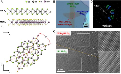
WSe2/MoS2 hetero-bilayer illustration, optical image, and TEM images. (A) Atomistic illustrations of the heterostructure of single-layer (SL) WSe2 on SL MoS2 with their respective lattice constants and a misalignment angle ϕ. (B) Optical microscope image of a WSe2/MoS2 hetero-bilayer on a Si/SiO2 substrate (260-nm SiO2). (C) HRTEM images of a boundary region of SL MoS2 and the hetero-bilayer, showing the resulting Moiré pattern. (D) The electron diffraction pattern of the hetero-bilayer shown in B, with the pattern of MoS2 and WSe2 indexed in green and blue colors, respectively.
To shed light on the electronic structure of the WSe2/MoS2 heterostack, we performed X-ray photoelectron spectroscopy (XPS). Specifically, we used a photoemission electron microscope (PEEM) with a high spatial resolution of 30 nm to discriminate between photoelectrons emitted from the WSe2 single layer, MoS2 single layer, and the WSe2/MoS2 hetero-bilayer, as illustrated in Fig. 2A (see Fig. S3 for details). In addition, by looking at the core-level photoelectrons, we achieved elemental and electronic selectivity that allows us to probe photoelectrons originating from the top layer of the hetero-bilayer and to directly quantify the potential difference between the WSe2 layer in the hetero-stack with respect to the WSe2 single-layer reference on the substrate. As shown in Fig. 2B, a peak shift of about −220 meV in binding energy (or +220 meV in kinetic energy) is evident in the W 4f core levels of the hetero-bilayer compared with the WSe2 single layer. The direction of the peak shift is consistent with a negative net charge on the WSe2 in the WSe2/MoS2 hetero-bilayer. However, a shift of +190 meV is observed in the Mo 3d core levels of the WSe2/MoS2 in Fig. 2C. Our PEEM results therefore indicate that the WSe2 layer has a negative net charge, whereas the MoS2 layer has a positive net charge as a result of contact potential. The hetero-bilayer can essentially be interpreted as being a 2D dipole, an atomically thin parallel plate capacitor with vdW gap with a built-in potential up to 400 meV, originating from the work function difference induced charge transfer between the two constituent single layers. The latter interpretation is also consistent with the p- and n-type character of WSe2 and MoS2, respectively (2, 3).
Fig. 2.
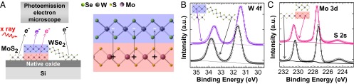
XPS core level shift analyses of WSe2/MoS2 heterostructures. (A) Sketch of the spatially resolved PEEM experiment. (B) Comparison of W 4f core level doublet from WSe2 and WSe2/MoS2 indicating a 220-meV shift to lower binding energy, corresponding to a negative net charge on the WSe2 top layer. (C) Comparison of Mo 3d core level doublet and S 2s singlet from MoS2 and WSe2/MoS2 indicating a shift of 190 meV to higher binding energy, corresponding to a positive net charge on MoS2. The single peak at 224.4–224.6 eV is identified as S 2s, which shows the same shift as Mo 3d, as expected.
To investigate the optoelectronic properties of the WSe2/MoS2 hetero-bilayer, we used photoluminescence (PL) and absorption spectroscopy. It is known that both single-layer WSe2 and MoS2 exhibit direct band gaps, whereas their bulk and homo-bilayer counterparts are indirect (1, 27). In agreement with previous work we observe strong excitonic PL peaks at 1.64 eV and 1.87 eV for single-layer WSe2 and MoS2, respectively (Fig. 3A). Note that single-layer WSe2 shows a 10–20 times higher PL intensity than single-layer MoS2, a result consistent with ref. 28. For the WSe2/MoS2 hetero-bilayer, we observe a peak at 1.55 eV, lying interestingly at a lower energy than for the two constituent single layers, as shown in Fig. 3A (with intensity ∼1.5 times higher than for single-layer MoS2). The appearance of a peak at such low energy was observed consistently for multiple (>10) samples, with peak energies ranging from 1.50 to 1.56 eV (Fig. S4). This distribution is attributed to sample-to-sample variations in interface quality and/or alignment angle ϕ. Of value in optoelectronics, an Urbach tail inverse slope, corresponding to the band edge sharpness of ∼30 meV/dec is extracted from the PL spectra (29, 30) (Fig. S5). The steep tail slopes of our hetero-bilayer prove that high-quality heterostructures with sharp band edges can be built at the single-layer limit using TMDC building blocks, which is a unique feature of this material system.
Fig. 3.
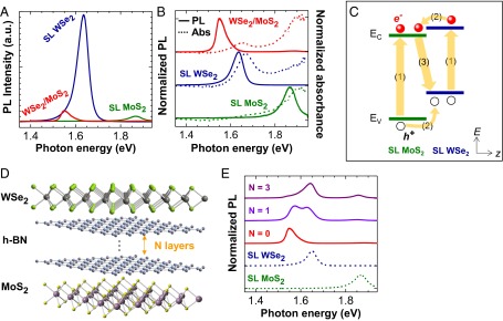
Photoluminescence and absorption from WSe2/MoS2 hetero-bilayers. (A) PL spectra of single-layer WSe2, MoS2, and the corresponding hetero-bilayer. (B) Normalized PL (solid lines) and absorbance (dashed lines) spectra of single-layer WSe2, MoS2, and the corresponding hetero-bilayer, where the spectra are normalized to the height of the strongest PL/absorbance peak. (C) Band diagram of WSe2/MoS2 hetero-bilayer under photo excitation, depicting (1) absorption and exciton generation in WSe2 and MoS2 single layers, (2) relaxation of excitons at the MoS2/WSe2 interface driven by the band offset, and (3) radiative recombination of spatially indirect excitons. (D) An atomistic illustration of the heterostructure of single-layer WSe2/single-layer MoS2 with few-layer h-BN spacer in the vdW gap. (E) Normalized PL spectra from single-layer WSe2/single-layer MoS2 heterostructure with n layers of h-BN (n = 0, 1, and 3).
The nature of the photoluminescence of the WSe2/MoS2 hetero-bilayer is intriguing. To better understand the electronic structure of the hetero-bilayer, we performed absorption measurements in the near-infrared and visible part of the spectrum using synchrotron light shown as dashed lines in Fig. 3B. The WSe2/MoS2 hetero-bilayer shows a first absorption peak at 1.65 eV and a second peak at 1.91 eV. These peaks closely coincide with the absorption peaks of single-layer WSe2 and MoS2, respectively. Interestingly, comparing the absorption spectra with the normalized PL data shown in Fig. 3B, we note that the hetero-bilayer exhibits a striking ∼100 meV shift between the PL and absorbance peaks. This large Stokes-like shift is consistent with a spatially indirect transition in a staggered gap (type II) heterostructure (31) (as shown in Fig. 3C). Our hetero-bilayers share certain similarities with organic semiconductor heterostructures in which donor and acceptor layers are also bound by weak intermolecular vdW forces (32). Similar to the optical processes in organic heterostructures, photons are absorbed in single-layer WSe2 and single-layer MoS2, generating excitons in both layers. Photo-excited excitons then relax at the MoS2/WSe2 interface, driven by the band offset as shown in Fig. 3C. That band offset is also consistent with the measured built-in electric field from PEEM. Owing to the energy lost to the band offset (Fig. 3C), the PL excitonic peak energy is lower than the excitonic band gaps of either material component. This 100-meV shift may be a balance between conduction band offset between the two monolayers versus diminished exciton binding energy associated with being spatially indirect. Note that in the hetero-bilayer we observe only a weak luminescence signal at the energies corresponding to the excitonic band gaps of single-layer MoS2 and WSe2, suggesting that the large majority of the photo-excited carriers are relaxed at the interface producing the highest luminescence for the spatially indirect recombination process.
To fine-tune the interlayer interaction in the WSe2/MoS2 hetero-bilayer, single- and few-layer sheets of hexagonal BN (h-BN) spacer layers were inserted into the vdW gap (Fig. 3D) using the same transfer technique. Fig. 3E shows the normalized PL of hetero-stacks with single- and trilayer h-BN spacers. Interlayer spatially indirect recombination becomes negligible for the sample with a trilayer h-BN spacer, as indicated by both the position and the intensity of the peak at 1.64 eV (Fig. 3E and Fig. S6), which are nearly the same as for single-layer WSe2. However, a single layer of h-BN does not fully suppress the interlayer interaction between WSe2 and MoS2. The results demonstrate that the interlayer coupling can be readily tuned by intercalation of dielectric layers and provide yet another degree of control in the vdW heterostructure properties.
Finally, we explored the carrier transport along the hetero-bilayer interface. A single flake consisting of single-layer WSe2 and MoS2, and an overlapping hetero-bilayer was made via the transfer process. The flake was dry etched into a long ribbon (Fig. 4A). A corresponding PL peak energy map is shown at the right edge of Fig. 4A, further depicting the ribbon structure by color coding of the luminescence energy. Multiple source/drain (S/D) metal electrodes were then fabricated by electron beam lithography and lift-off on each region of the ribbon (see Figs. S7 and S8 for details). The Si/SiO2 substrate serves as the global back gate, with 260 nm gate oxide thickness. As expected single-layer MoS2 and WSe2 devices exhibit n- and p-channel characteristics, respectively (Fig. S9), consistent with previous reports (2, 3). However, the device consisting of one contact on the monolayer WSe2 and the other on monolayer MoS2, with the two layers overlapping in the central region (Fig. 4B) exhibits a distinct rectifying behavior (Fig. 4C and Fig. S10), consistent with type II band alignment of the hetero-bilayer. The rectification provides additional evidence for electrical coupling and proper contact potential between the two constituent layers. This behavior is consistent with previous work on TMDC/nanotubes (33) and TMDC/III-V heterostructures (34), which had shown that electrically active vdW interfaces can be achieved from TMDC components. The work here highlights the ability to engineer a novel class of electronic and optoelectronic devices by vdW stacking of the desired layered chalcogenide components with molecular-scale thickness control.
Fig. 4.

Electrical transport across the WSe2/MoS2 hetero-interface. (A) Optical microscope image of a device encompassing single-layer WSe2, WSe2/MoS2 hetero-bilayer, and single-layer MoS2 on a Si/SiO2 substrate. Electrodes are numbered 1–7 from bottom to top. (Right) A color-coded PL peak energy map. (Scale bar, 2 µm.) (B) A qualitative band diagram of the single-layer WSe2/hetero-bilayer/single-layer MoS2 device, corresponding to the device between electrodes 2 and 3. (C) I-V characteristic when measuring between electrodes 2 and 3, with 2 grounded and 3 biased. A back-gate voltage of 50 V was applied to reduce the contact resistance to MoS2 and patterned NO2 doping was used near the WSe2 contact for reducing the contact resistance.
In summary, we have fabricated and characterized an artificial vdW heterostructure by stacking monolayer TMDC building blocks and achieved electronic coupling between the two 2D semiconductor constituents. Strong PL with a large Stokes-like shift was observed from the WSe2/MoS2 hetero-bilayer, consistent with spatially indirect luminescence from a type II heterostructure. We anticipate that our result will trigger subsequent studies focused on the bottom-up creation of new heterostructures by varying chemical composition, interlayer spacing, and angular alignment. In addition, the focus will be on the fabrication of vdW semiconductor heterostructure devices with tuned optoelectronic properties from customized single-layer components. Particularly, electroluminescene efficiency of vdW heterostructures needs to be explored experimentally to examine their viability for use as nanoscale light-emitting/lasing devices.
Supplementary Material
Acknowledgments
Materials characterization of this work was supported by the director, Office of Science, Office of Basic Energy Sciences, Materials Sciences and Engineering Division of the US Department of Energy (DOE) under Contract DE-AC02-05CH11231. The device fabrication and characterization was supported by the National Science Foundation (NSF) E3S center. The transmission electron microscopy work was performed at the National Center for Electron Microscopy, Lawrence Berkeley National Laboratory, which is supported by US DOE Contract DE-AC02-05CH11231. The absorption measurements were performed at the Advanced Light Source, Lawrence Berkeley National Laboratory. C. Carraro and R.M. acknowledge support from NSF Grant EEC-0832819 (Center of Integrated Nanomechanical Systems).
Footnotes
The authors declare no conflict of interest.
This article contains supporting information online at www.pnas.org/lookup/suppl/doi:10.1073/pnas.1405435111/-/DCSupplemental.
References
- 1.Mak KF, Lee C, Hone J, Shan J, Heinz TF. Atomically thin MoS2: A new direct-gap semiconductor. Phys Rev Lett. 2010;105(13):136805. doi: 10.1103/PhysRevLett.105.136805. [DOI] [PubMed] [Google Scholar]
- 2.Radisavljevic B, Radenovic A, Brivio J, Giacometti V, Kis A. Single-layer MoS2 transistors. Nat Nanotechnol. 2011;6(3):147–150. doi: 10.1038/nnano.2010.279. [DOI] [PubMed] [Google Scholar]
- 3.Fang H, et al. High-performance single layered WSe2 p-FETs with chemically doped contacts. Nano Lett. 2012;12(7):3788–3792. doi: 10.1021/nl301702r. [DOI] [PubMed] [Google Scholar]
- 4.Wang H, et al. Integrated circuits based on bilayer MoS2 transistors. Nano Lett. 2012;12(9):4674–4680. doi: 10.1021/nl302015v. [DOI] [PubMed] [Google Scholar]
- 5.Zeng H, Dai J, Yao W, Xiao D, Cui X. Valley polarization in MoS2 monolayers by optical pumping. Nat Nanotechnol. 2012;7(8):490–493. doi: 10.1038/nnano.2012.95. [DOI] [PubMed] [Google Scholar]
- 6.Jones AM, et al. Optical generation of excitonic valley coherence in monolayer WSe2. Nat Nanotechnol. 2013;8(9):634–638. doi: 10.1038/nnano.2013.151. [DOI] [PubMed] [Google Scholar]
- 7.Geim AK, Grigorieva IV. Van der Waals heterostructures. Nature. 2013;499(7459):419–425. doi: 10.1038/nature12385. [DOI] [PubMed] [Google Scholar]
- 8.Yu WJ, et al. Vertically stacked multi-heterostructures of layered materials for logic transistors and complementary inverters. Nat Mater. 2013;12(3):246–252. doi: 10.1038/nmat3518. [DOI] [PMC free article] [PubMed] [Google Scholar]
- 9.Georgiou T, et al. Vertical field-effect transistor based on graphene-WS2 heterostructures for flexible and transparent electronics. Nat Nanotechnol. 2013;8(2):100–103. doi: 10.1038/nnano.2012.224. [DOI] [PubMed] [Google Scholar]
- 10.Yu WJ, et al. Highly efficient gate-tunable photocurrent generation in vertical heterostructures of layered materials. Nat Nanotechnol. 2013;8(12):952–958. doi: 10.1038/nnano.2013.219. [DOI] [PMC free article] [PubMed] [Google Scholar]
- 11.Britnell L, et al. Strong light-matter interactions in heterostructures of atomically thin films. Science. 2013;340(6138):1311–1314. doi: 10.1126/science.1235547. [DOI] [PubMed] [Google Scholar]
- 12.Wilson J, Yoffe A. The transition metal dichalcogenides discussion and interpretation of the observed optical, electrical and structural properties. Adv Phys. 1969;18(73):193–335. [Google Scholar]
- 13.Terrones H, López-Urías F, Terrones M. Novel hetero-layered materials with tunable direct band gaps by sandwiching different metal disulfides and diselenides. Sci Rep. 2013;3:1549. doi: 10.1038/srep01549. [DOI] [PMC free article] [PubMed] [Google Scholar]
- 14.Kang J, Li J, Li S-S, Xia J-B, Wang L-W. Electronic structural Moiré pattern effects on MoS2/MoSe2 2D heterostructures. Nano Lett. 2013;13(11):5485–5490. doi: 10.1021/nl4030648. [DOI] [PubMed] [Google Scholar]
- 15.Kośmider K, Fernández-Rossier J. Electronic properties of the MoS2-WS2 heterojunction. Phys Rev B. 2013;87(7):075451. [Google Scholar]
- 16.Komsa H-P, Krasheninnikov AV. Electronic structures and optical properties of realistic transition metal dichalcogenide heterostructures from first principles. Phys Rev B. 2013;88(8):085318. [Google Scholar]
- 17.Gong C, et al. Band alignment of two-dimensional transition metal dichalcogenides: Application in tunnel field effect transistors. Appl Phys Lett. 2013;103(5):053513. [Google Scholar]
- 18.Dean CR, et al. Boron nitride substrates for high-quality graphene electronics. Nat Nanotechnol. 2010;5(10):722–726. doi: 10.1038/nnano.2010.172. [DOI] [PubMed] [Google Scholar]
- 19.Ponomarenko L, et al. Tunable metal-insulator transition in double-layer graphene heterostructures. Nat Phys. 2011;7(12):958–961. [Google Scholar]
- 20.Haigh SJ, et al. Cross-sectional imaging of individual layers and buried interfaces of graphene-based heterostructures and superlattices. Nat Mater. 2012;11(9):764–767. doi: 10.1038/nmat3386. [DOI] [PubMed] [Google Scholar]
- 21.Britnell L, et al. Field-effect tunneling transistor based on vertical graphene heterostructures. Science. 2012;335(6071):947–950. doi: 10.1126/science.1218461. [DOI] [PubMed] [Google Scholar]
- 22.Gorbachev R, et al. Strong Coulomb drag and broken symmetry in double-layer graphene. Nat Phys. 2012;8:896–901. [Google Scholar]
- 23.Hunt B, et al. Massive Dirac fermions and Hofstadter butterfly in a van der Waals heterostructure. Science. 2013;340(6139):1427–1430. doi: 10.1126/science.1237240. [DOI] [PubMed] [Google Scholar]
- 24.Ponomarenko LA, et al. Cloning of Dirac fermions in graphene superlattices. Nature. 2013;497(7451):594–597. doi: 10.1038/nature12187. [DOI] [PubMed] [Google Scholar]
- 25.Dean CR, et al. Hofstadter’s butterfly and the fractal quantum Hall effect in moiré superlattices. Nature. 2013;497(7451):598–602. doi: 10.1038/nature12186. [DOI] [PubMed] [Google Scholar]
- 26.Yankowitz M, et al. Emergence of superlattice Dirac points in graphene on hexagonal boron nitride. Nat Phys. 2012;8(5):382–386. [Google Scholar]
- 27.Zeng H, et al. Optical signature of symmetry variations and spin-valley coupling in atomically thin tungsten dichalcogenides. Sci Rep. 2013;3:1608. doi: 10.1038/srep01608. [DOI] [PMC free article] [PubMed] [Google Scholar]
- 28.Zhao W, et al. Evolution of electronic structure in atomically thin sheets of WS2 and WSe2. ACS Nano. 2013;7(1):791–797. doi: 10.1021/nn305275h. [DOI] [PubMed] [Google Scholar]
- 29.Van Roosbroeck W, Shockley W. Photon-radiative recombination of electrons and holes in germanium. Phys Rev. 1954;94(6):1558. [Google Scholar]
- 30.Kost A, Lee H, Zou Y, Dapkus P, Garmire E. Band-edge absorption coefficients from photoluminescence in semiconductor multiple quantum wells. Appl Phys Lett. 1989;54(14):1356–1358. [Google Scholar]
- 31.Wilson BA. Carrier dynamics and recombination mechanisms in staggered-alignment heterostructures. IEEE J Quantum Electron. 1988;24(8):1763–1777. [Google Scholar]
- 32.Li G, Zhu R, Yang Y. Polymer solar cells. Nat Photonics. 2012;6(3):153–161. [Google Scholar]
- 33.Jariwala D, et al. Gate-tunable carbon nanotube-MoS2 heterojunction p-n diode. Proc Natl Acad Sci USA. 2013;110(45):18076–18080. doi: 10.1073/pnas.1317226110. [DOI] [PMC free article] [PubMed] [Google Scholar]
- 34.Chuang S, et al. Near-ideal electrical properties of InAs/WSe2 van der Waals heterojunction diodes. Appl Phys Lett. 2013;102(24):242101. [Google Scholar]
Associated Data
This section collects any data citations, data availability statements, or supplementary materials included in this article.