Abstract
A membrane that allows selective transport of molecular species requires precise engineering on the nanoscale. Membrane permeability can be tuned by controlling the physical structure and surface chemistry of the pores. Here, a combination of electron beam and optical lithography, along with cryogenic deep reactive ion etching, has been used to fabricate silicon membranes that are physically robust, have uniform pore sizes, and are directly integrated into a microfluidic network. Additional reductions in pore size were achieved using plasma enhanced chemical vapor deposition and atomic layer deposition of silicon dioxide to coat membrane surfaces. Cross sectioning of the membranes using focused ion beam milling was used to determine the physical shape of the membrane pores before and after coating. Functional characterization of the membranes was performed by using quantitative fluorescence microscopy to document the transport of molecular species across the membrane.
INTRODUCTION
The ability to tailor membrane features, including overall width, pore size, and density, is essential in the development of synthetic membranes for applications in molecular separation or sieving. Tuning these physical characteristics allows one to tailor the flux of materials based on specific needs, simultaneously allowing modulation of hydrodynamic resistance and physical exclusion. By modulating pore size at the nanoscale, size-selective transport allowing the retention of large molecules while allowing small molecules to freely traverse the membrane is possible.1 Furthermore, by chemically functionalizing the membrane surface, chemically based separations can be achieved.2, 3
Integrating nanoporous membranes within a microfluidic network provides a model test platform for understanding transport and monitoring the flux of molecules across the membrane. While previous studies have described the fabrication and use of synthetic membranes within microfluidic test platforms, most rely on the assembly of these membranes within microchannels rather than direct integration. A common approach to create such a membrane is the use of natural membrane components, i.e., lipid bilayers, on a substrate.4, 5, 6, 7 The drawbacks of using lipid bilayers are their poor long-term stability and challenges in their integration with inorganic materials. Other common materials, such as nuclear track-etched polycarbonate,2, 8, 9 porous alumina,2, 10, 11 silicon,3, 12 silicon nitride,13, 14 and carbon nanotubes,15 have served as freestanding membranes. For these types of membranes, separate fluidic structures need to be fabricated and assembled with the membranes to create functional devices. Examples where integration of a membrane within a microfluidic network has been achieved include the use of silicon,16in situ polymerized materials,17 and vertically aligned carbon nanofibers as membrane materials.18, 19
Here, we describe the fabrication of a nanoporous membrane within a microfluidic platform that allows tunable transport of molecular species between two parallel microfluidic channels. The fabrication process allows precise control of pore geometry, density, and surface chemistry, which can all be tuned to modulate the flux of different molecular species based on size, charge, and chemical affinity. The membrane is physically robust and directly integrated within the microfluidic network. The physical characteristics of the pore, including pore length, width, and density are defined using electron beam lithography. Photolithography is used to define the geometry of the microfluidic network. The nano- and microscale patterns are simultaneously etched into the silicon substrate using deep reactive ion etching (DRIE). Modulation of the pore size and surface chemistry is carried out by coating the membrane surface with silicon dioxide using plasma enhanced chemical vapor deposition (PECVD) and/or atomic layer deposition (ALD). The three-dimensional geometry of the membrane pore structure was analyzed by scanning electron microscopy (SEM) in conjunction with focused ion beam processed cross-sections. Functional characterization of the membranes was performed by using quantitative fluorescence microscopy to document the transport of molecular species across the membrane.
FABRICATION
Figure 1 illustrates the fabrication process of the nanoporous membrane. Standard 100 mm silicon wafers with a orientation were used as membrane substrates. Wafers were spin-coated with PMMA 495 A4 electron beam resist (Microchem Corp., Newton, MA) at 2500 rpm for 45 s and baked on a hotplate for 5 min at . Electron beam lithography was performed with a JEOL JBX9300-FS system operating at 100 kV acceleration voltage and 2 nA beam current to define the geometry of the membrane, including the 200 nm pore width. The dose used in this process was . Patterned wafers were developed in 1:3 methyl isobutyl ketone:isopropyl alcohol (IPA) for 1 min, rinsed with IPA, and dried with nitrogen, followed by exposure to oxygen plasma for 6 s at 100 W, 10 SCCM (SCCM denotes standard cubic centimeter at STP), and 150 mT. A lift-off process was carried out following deposition of 15 nm chromium by electron beam evaporation, leaving a chromium etch mask only on the areas exposed by the electron beam [Fig. 1a].
Figure 1.

(Color online) Fabrication of a nanostructured silicon membrane: (a) e-beam lithography for membrane patterning, followed by Cr deposition and lift-off; (b) optical lithography patterning defines the microfluidic network; (c) a single cryogenic deep reactive ion-etch is used to transfer the pattern into a silicon substrate; (d) PDMS sealing.
Conventional contact alignment optical lithography was used to define the integrated, parallel, wide microfluidic channels as well as 1 mm diameter inlets and outlets. MicroPrime™ MP-P20 (Shin-Etsu MicroSi, Inc., Phoenix, AZ) was spin-coated at 6000 rpm as an adhesion promoter prior to the photoresist coating. We used a negative photoresist, JSR Micro NFR 016 D2 55cP (JSR Micro Inc., Sunnyvale, CA), which was resistant to cracking during the cryogenic etching process. Wafers were baked on a hotplate at for 90 s, exposed for 5 s, followed by a postexposure bake on a hotplate at for 90 s. The development process was carried out in CD26 developer ( tetramethylammonium hydroxide, MicroChem Corp., Newton, MA) for 15 s, rinsed with de-ionized water, and dried with nitrogen. After 30 s exposure to oxygen plasma at 400 W to remove any resist residue left on the exposed areas, wafers were baked at for 3 min [Fig. 1b].
The membrane and the microfluidic channels were etched using a cryogenic silicon etching process in an inductively coupled plasma ion etching system (Oxford Plasmalab 100). The process was carried out in a mixture of and gases at . Control of oxygen content in the flow allows balance between etching and sidewall passivation on the membrane structure, affecting the ratio of pore depth to membrane height. Removal of the photoresist was accomplished by soaking the substrate in n-methyl-pyrrolidinone at [Fig. 1c].
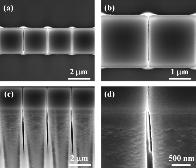
Silicon dioxide was conformally coated on the membrane structure via PECVD (Oxford PlasmaLab 100) or ALD (Oxford FlexAL). Silicon dioxide was chosen for coating of the pores because it can be easily modified using silanization processes in future applications to enhance membrane selectivity to charged species. By adjusting the duration of deposition time used for PECVD or the number of deposition cycles used for ALD, control of the pore geometry was achieved. SEM images of the fabricated nanostructure membrane are shown in Fig. 2.
Figure 2.
SEM images of a nanostructured membrane in silicon: [(a) and (b)] top view; [(c) and (d)] side view (sample tilted by 30°).
The microfluidic channels were sealed with a 10:1 mixture of polydimethylsiloxane (PDMS) prepolymer and curing agent (Sylgard 184, Dow Corning) [Fig. 1d]. After degassing, PDMS was cured at for 1 h. Cured PDMS sections were cut to match the size of the silicon microfluidic chip, which measured approximately 4 cm long and 1.5 cm wide. Two inlets and two outlets were punched through the PDMS using a Harris Uni-core tool with a tip diameter of 0.75 mm (Tedpella Inc., Redding, CA). The solution was introduced into the microchannels using a 0.03 in. outer diameter Tygon microbore tubing.
DISCUSSION
Tuning membrane and pore features
The membrane height and the pore depth were determined by deep reactive ion etching duration and process conditions. The etch rate and sidewall profile were functions of and flow rates at cryogenic temperatures . The addition of with creates passivation layers on the etched structure sidewall, resulting in anisotropic etching.20 During the membrane fabrication process, the oxygen flow rate controlled the anisotropy of the etch process and significantly impacted the resulting geometry of the membrane features. Circular membranes, having pores identical to linear membranes, were created by carrying out DRIE using different oxygen flow rates (Fig. 3). Although these membranes had a circular shape, the large radius of curvature to width ratio (10:1) resulted in negligible differences between these circular membrane structures and the linear membranes described in greater detail here. To assess the effects of DRIE oxygen content on pore geometry, the flow rate, etching temperature, and etch duration were fixed (80 SCCM, , and 5 min). The oxygen flow rate was varied from 10, 11, 12, to 14 SCCM. At 10 SCCM flow rate, etching was more aggressive compared with other flow rates, as demonstrated by the depth of the outer membrane pores. Some variability in pore depth was also observed. A similar trend was observed at 11 SCCM . At a flow rate of 14 SCCM , the pores were shallow and excess passivating polymer layers deposited on the sidewall were observable. For the fabrication of the tested membrane structures, an oxygen flow rate of 12 SCCM was selected due to its balance of pore depth and uniformity. An etching time of 5 min under these conditions resulted in a membrane height of approximately . In Fig. 3, the bulging area below each pore was due to the excess passivating polymer that deposited as etching gases were consumed locally at each pore site during the etch process.
Figure 3.
Effect of oxygen content during cryogenic deep reactive ion etching on the nanostructured membrane in silicon: (a) 10, (b) 11, (c) 12, and (d) 14 SCCM flow rates.
Physical and functional characterization
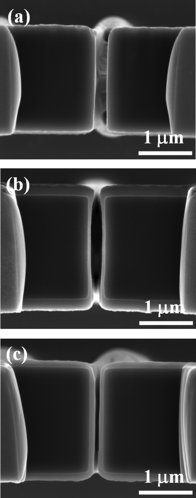
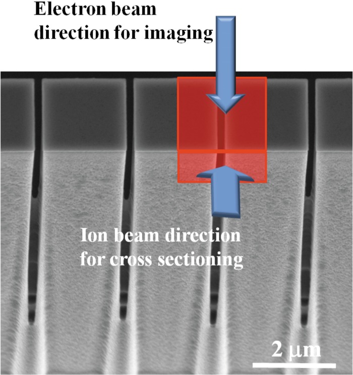
Some variation of pore width was observable from the top to the bottom of the pore and along the thickness of the membrane wall. Because of the etching profile, it was difficult to determine the size and shape of the pore aperture using conventional SEM. This was especially difficult after the pores were coated with silicon dioxide. Cross-sections of the pores were created by successive milling using ions at 30 kV and 0.1 nA. The cross-sections facilitated direct imaging of individual pores, ultimately allowing three-dimensional reconstruction of the pore structure for evaluation of the coating conformality. The milling process was carried out by orienting the ion beam perpendicular to the membrane wall. Imaging of the process was carried out from a top view of the cross-section (Fig. 4). Examples of cross-sections of bare silicon membrane and silicon dioxide coated membranes (PECVD and ALD) are shown in Figs. 5a, 5b, 5c, respectively. Atomic layer deposition provided a conformal and even coating when compared to PECVD. However, both techniques allowed the controllable reduction in the minimum pore aperture size. Work is ongoing to assess the impact of pore geometry on diffusion mediated flux and membrane selectivity.
Figure 4.
(Color online) Ion milling was performed perpendicularly to the membrane wall; result of the cross sectioning observed from the top view.
Figure 5.

SEM images of cross section of the membrane in (a) bare silicon, (b) silicon coated with PECVD , and (c) silicon coated with ALD .
Demonstrations of fluid flow through the microfluidic network and the diffusion mediated exchange of fluorescein across the membrane are shown in Fig. 6. An Olympus BX51 upright microscope with Zeiss AxioCam HRC charge coupled device camera controlled by OPENLAB software (Improvision, UK) was used for collecting fluorescent images. One inlet of the coupled microfluidic channels was filled with fluorescein and Tris buffer (left), while the other inlet was filled with Tris buffer only (right). The flow rate for both channels was . The silicon membrane used in this experiment was coated with , with pores having an average limiting aperture of approximately 100 nm. This pore width was much larger than the fluorescein molecular size (radius of 0.45 nm), allowing the molecules to diffuse easily across the membrane. The steady state concentration profile of fluorescein along the length of the membrane [Fig. 6b], corresponding to the fluorescence intensity gradient captured using fluorescence microscopy [Fig. 6a], provided a quantitative measure of molecular flux across the membrane. Future studies will focus on examining the effects of molecular charge, length, size, and flow on this molecular exchange.
Figure 6.
(Color online) Fluid flow through the microfluidic network and diffusion mediated exchange across the nanoporous membrane: (a) diffusion profile observed under fluorescence microscope; (b) plot of concentration profile along the microfluidic channel.
SUMMARY
Multiscale fabrication techniques were used to fabricate a physically robust nanostructured membrane integrated within a microfluidic network. Control of the membrane porosity, through modulation of pore density, geometry, and surface chemistry, was provided throughout the fabrication process. The pore width and density were defined by e-beam lithography, which can be readily tailored for specific applications. The membrane height and pore depth were dependent on the cryogenic deep reactive ion etching conditions. It was shown that these etch conditions, specifically oxygen content, could be modified to realize membranes with varying ratios of pore depth to membrane height. Further control of pore width and surface properties was achieved by depositing silicon dioxide on the membrane surface using either PECVD or ALD techniques. Physical characterization of membrane structures using ion milling was used to characterize the internal pore geometry and clearly showed the conformality of coatings achieved using ALD compared with PECVD. Functional characterization of membrane structures was carried out using quantitative fluorescence imaging techniques.
The ability to tune the porosity and the surface chemistry of a membrane within a microfluidic network opens the door to tailoring molecular exchange between functional compartments of a microfluidic system without introducing hydrodynamic effects. The control of pore uniformity, size, and surface properties, as well as the ability to physically measure pore geometry, is essential to developing a fundamental understanding of the impact of such parameters on selective molecular transport. Future work will include examinations of controlled transport based on both molecular size and charge using chemically functionalized membrane structures with pore sizes tailored for specific classes of molecules.
ACKNOWLEDGMENT
This research was supported by NIH Grant No. EB000657. S.T.R., J.D.F., and M.J.D. would like to acknowledge funding from the Center for Nanophase Materials Sciences, which is sponsored at Oak Ridge National Laboratory by the Division of Scientific User Facilities, U.S. Department of Energy. This work was performed at the Oak Ridge National Laboratory, managed by UT-Battelle, LLC, for the U.S. DOE under Contract No. DE-AC05-00OR22725. The nanofabrication performed in this manuscript was carried out at the Nanofabrication Research Facility at the Center for Nanophase Materials Sciences as part of user project CNMS 2010-101.
References
- Retterer S. T., Suiti P., Choi C. -K., Thomas D. K., and Doktycz M. J., Lab Chip 10, 1174 (2010). 10.1039/b921592a [DOI] [PMC free article] [PubMed] [Google Scholar]
- Martin C. R., Nishizawa M., Jirage K., Kang M., and Lee S. B., Adv. Mater. 13, 1351 (2001). [DOI] [Google Scholar]
- Striemer C. C., Gaborski T. R., McGrath J. L., and Fauchet P. M., Nature (London) 445, 749 (2007). 10.1038/nature05532 [DOI] [PubMed] [Google Scholar]
- Sackmann E., Science 271, 43 (1996). 10.1126/science.271.5245.43 [DOI] [PubMed] [Google Scholar]
- Tamm L. K. and McConnell H. M., Biophys. J. 47, 105 (1985). 10.1016/S0006-3495(85)83882-0 [DOI] [PMC free article] [PubMed] [Google Scholar]
- Cornell B. A., Braach-Maksvytis V. L. B., King L. G., Osman P. D. J., Raguse B., Wieczorek L., and Pace R. J., Nature (London) 387, 580 (1997). 10.1038/42432 [DOI] [PubMed] [Google Scholar]
- Groves J. T. and Boxer S. G., Acc. Chem. Res. 35, 149 (2002). 10.1021/ar950039m [DOI] [PubMed] [Google Scholar]
- Kuo T. C., Cannon D. M., Shannon M. A., Bohn P. W., and Sweedler J. V., Sens. Actuators, A 102, 223 (2003). 10.1016/S0924-4247(02)00394-1 [DOI] [Google Scholar]
- D. M.Cannon, Jr., Kuo T. -C., Bohn P. W., and Sweedler J. V., Anal. Chem. 75, 2224 (2003). 10.1021/ac020629f [DOI] [PubMed] [Google Scholar]
- Trofin L., Lee S. B., Mitchell D. T., and Martin C. R., J. Nanosci. Nanotechnol. 4, 239 (2004). 10.1166/jnn.2004.031 [DOI] [PubMed] [Google Scholar]
- Steinle E. D., Mitchell D. T., Wirtz M., Lee S. B., Young V. Y., and Martin C. R., Anal. Chem. 74, 2416 (2002). 10.1021/ac020024j [DOI] [PubMed] [Google Scholar]
- Desai T. A., Hansford D., and Ferrari M., J. Membr. Sci. 159, 221 (1999). 10.1016/S0376-7388(99)00062-9 [DOI] [Google Scholar]
- Tong H. D., Jansen H. V., Gadgil V. J., Bostan C. G., Berenschot E., van Rijn C. J. M., and Elwenspoek M., Nano Lett. 4, 283 (2004). 10.1021/nl0350175 [DOI] [Google Scholar]
- Vlassiouk I., Apel P. Y., Dmitriev S. N., Healy K., and Siwy Z. S., Proc. Natl. Acad. Sci. U.S.A. 106, 21039 (2009). 10.1073/pnas.0911450106 [DOI] [PMC free article] [PubMed] [Google Scholar]
- Majumder M., Stinchcomb A., and Hinds B. J., Life Sci. 86, 563 (2010). 10.1016/j.lfs.2009.04.006 [DOI] [PMC free article] [PubMed] [Google Scholar]
- Turner S. W., Perez A. M., Lopez A., and Craighead H. G., J. Vac. Sci. Technol. B 16, 3835 (1998). 10.1116/1.590419 [DOI] [Google Scholar]
- Song S., Singh A. K., and Kirby B. J., Anal. Chem. 76, 4589 (2004). 10.1021/ac0497151 [DOI] [PubMed] [Google Scholar]
- Fletcher B. L., Hullander E. D., Melechko A. V., McKnight T. E., Klein K. L., Hensley D. K., Morrell J. L., Simpson M. L., and Doktycz M. J., Nano Lett. 4, 1809 (2004). 10.1021/nl0493702 [DOI] [Google Scholar]
- Fowlkes J. D., Fletcher B. L., Retterer S. T., Melechko A. V., Simpson M. L., and Doktycz M. J., Nanotechnology 19, 415301 (2008). 10.1088/0957-4484/19/41/415301 [DOI] [PMC free article] [PubMed] [Google Scholar]
- de Boer M. J., Gardeniers J. G. E., Jansen H. V., Smulders E., Gilde M. -J., Roelofs G., Sasserath J. N., and Elwenspoek M., J. Microelectromech. Syst. 11, 385 (2002). 10.1109/JMEMS.2002.800928 [DOI] [Google Scholar]


