Abstract
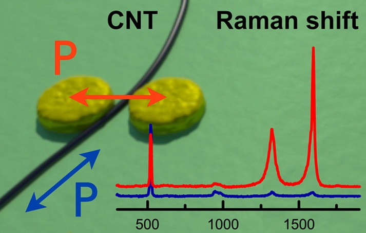
We realize the coupling of carbon nanotubes as a one-dimensional model system to near-field cavities for plasmon-enhanced Raman scattering. Directed dielectrophoretic assembly places single-walled carbon nanotubes precisely into the gap of gold nanodimers. The plasmonic cavities enhance the Raman signal of a small nanotube bundle by a factor of 103. The enhanced signal arises exclusively from tube segments within the cavity as we confirm by spatially resolved Raman measurements. Through the energy and polarization of the excitation we address the extrinsic plasmonic and the intrinsic nanotube optical response independently. For all incident light polarizations, the nanotube Raman features arise from fully symmetric vibrations only. We find strong evidence that the signal enhancement depends on the orientation of the carbon nanotube relative to the cavity axis.
Keywords: Raman spectroscopy, enhancement, plasmonic cavity, carbon nanotubes, dielectrophoresis
Optical coupling between light and matter in the nanoscale regime is of key interest for fundamental reasearch as well as applications in nanotechnology. It is studied by investigating metallic nanophotonic systems, that are based on field enhancement at optical wavelengths. Phenomena such as enhanced harmonic generation,1,2 plasmonic waveguides3,4 or plasmonic sensing5 are based on surface plasmon polaritons and localized surface plasmon resonances (LSPRs). The most spectacular application of LSPRs is surface-enhanced Raman scattering (SERS), where the compression of light into subwavelength volumes induces signal enhancements by several orders of magnitude.6−8 The challenges and findings in surface- and plasmon-enhanced Raman scattering naturally depend on two fundamental aspects: The type of scatterer used in the experiment and controlling its interface with a plasmonic hotspot.
Historically, molecules have been the prime candidate for investigating SERS, leading to the discovery of the effect9,10 and to the detection of single molecules.11−13 The precise location of a molecule with respect to a plasmonic hot spot, the orientation of the emitting dipole, and the absence of additional scatterers in the vicinity of the hotspot remain impossible to control experimentally. For single-walled carbon nanotubes (SWCNTs), in contrast its location and orientation with respect to a plasmonic hotspot can be readily obtained experimentally due to their one-dimensional nature. Nanotubes are chemically inert; their optical and vibrational properties are well-known. Beyond employing carbon nanotubes as a model system to investigate the mechanism of plasmonic enhancement in Raman scattering,14,15 they serve as an established platform to investigate the fundamental physics of quantum systems.16
An ideal interface between a near-field hotspot and a nanotube should combine high-field enhancement and the possibility to alter its optical response. The nanotube must be placed with extremely high precision and predefined orientation. Here we suggest to use dielectrophoretic deposition (DEP) of carbon nanotubes for the assembly of nanoplasmonic-nanotube systems by directing the tubes onto Au plasmonic antennas. We construct a system where a small carbon nanotube bundle is oriented orthogonal to a nanoscale plasmonic cavity. Light of two wavelengths and two orthogonal polarizations allows us to independently switch on and off the optical response of both the nanotube and the cavity. This interface gives us both a spatial and spectroscopic built-in calibration to probe fundamental aspects of the light-matter interaction in the nanoscale.
DEP offers a scalable and self-limiting bottom-up route for the directed assembly of CNTs17−19 as schematized in Figure 1a. An alternating current (ac) electric field at radio frequencies is applied between electrode pairs within a large array, while a droplet of CNT solution is placed on top. As the nanotubes possess a higher polarizability than the surrounding liquid, they experience a force directed toward the region of higher field strength, which occurs in between the electrodes, causing them to deposit there. The dielectrophoretic forces bias the nanotube deposition such that the tubes are (i) preferentially deposited between the electrodes where we place the plasmonic structures, (ii) oriented along the axis connecting the electrode pair, and (iii) prevented from coiling up.
Figure 1.
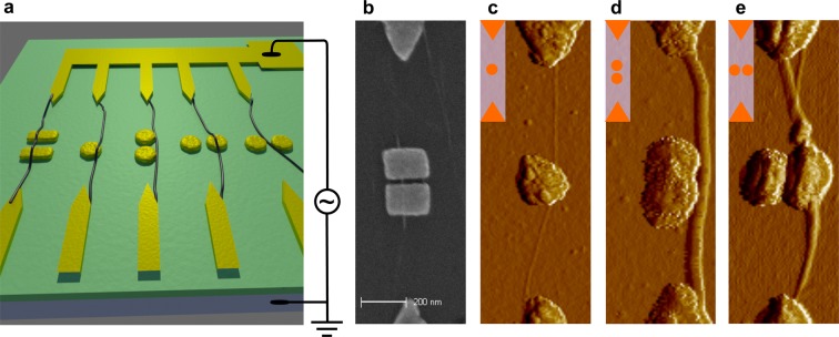
(a) Schematic of plasmonic antennas placed between interconnected biased electrodes and counter electrodes (yellow, in the front) that are capacitively coupled to the p-type silicon substrate (blue) via 290 nm of SiO2 (green). Carbon nanotubes dispersed in aqueous solution assemble between the electrodes due to dielectrophoretic forces and form nanoplasmonic-nanotube systems shown in the form of SEM (b) and AFM error images (c–e). CNTs may be suspended over a cavity formed by rods (b), cross a nanodisk (c,e) or be placed next to a plasmonic structure (d).
We constructed various interfaces by tailoring the shape, geometry, and composition of the nanostructures. In Figure 1b, a tube is placed across a plasmonic cavity formed by rods. It is suspended over the cavity and between the rod edges and the substrate as indicated by bright color in the scanning electron microscopy (SEM) image. Nanotubes may also be placed on top of a single nano disk, on top of one nano disk of a plasmonic dimer, and next to a dimer structure. The corresponding atomic force microscopy (AFM) error images are shown in Figure 1c–e. Further details on the nanotube deposition are given in the Supporting Information S1.
The ideal nanotube–nanoplasmonic interface as described before is realized in Figure 2a. Here, a small CNT bundle is placed in a plasmonic cavity that is formed by two nanodisks shown in Figure 2b before tube deposition. Height profiles at different positions in Figure 2c reveal thicknesses between 4 and 5 nm. We refer to this small nanotube bundle as CNT-B. Note that we can distinguish by AFM between a nanotube placed in a gap and a nanotube crossing a plasmonic particle as is the case in Figure 1d. The absence of those topographic features in Figure 2 confirms the location of CNT-B inside the cavity. The immediate surrounding of the cavity is free of additional nanotubes, which may otherwise hamper optical characterization.
Figure 2.
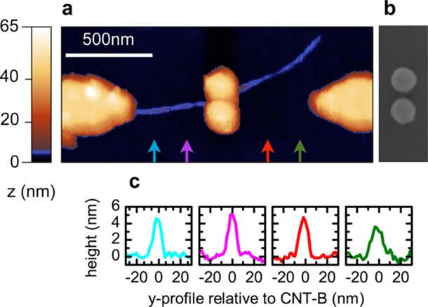
(a) AFM image of small carbon nanotubes bundle successfully placed in the cavity formed by two closely spaced Au nano disks. Topographic feature of the CNT are highlighted by introducing a mixing color (blue). (b) SEM image of nano disks before CNT deposition. Colored arrows in (a) indicate the position of the height profiles shown in (c).
The dimer in Figure 2a,b consists of two disks with a diameter of ∼100 nm and an interparticle distance of ∼25 nm. The dimensions and the geometry are designed to provide optimum enhancement for an excitation wavelength of 633 nm employed in the Raman scattering experiments. We characterize the plasmonic properties of the dimer using polarized dark-field spectroscopy before nanotube deposition. Spectra are acquired at separated, spatially isolated dimers to avoid contributions from the electrode tips. AFM and SEM pictures taken at multiple locations within and outside the electrode array confirm the structural homogeneity of the plasmonic dimers. A representative dark-field spectrum is shown in Figure 3a. Here, the polarization Py of the illumination source is set along the y-direction within our laboratory frame and corresponds to the dimer axis. The scattering maximum is located at 600 nm, which is in agreement with literature values for Au dimers of comparable diameter and gap size with the given polarization.20 Compared to the scattering maximum, the near-field resonance is red shifted,21 thereby providing a good match with an excitation of 633 nm. The frequency and strength of the resonances depend strongly on the polarization. For Py, the nanodisks are coupled via their near-field. The dominating surface plasmon excitation is of dipolar nature, leading to high near-fields localized in a sub wavelength volume in the gap.
Figure 3.
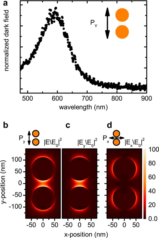
(a) Polarized dark field spectra of the nanodisk dimer. (b) Simulated near-field enhancement |E/E0|2 for Py. The corresponding component |Ey/E0|2 polarized in y-direction is shown in (c). (d) |E/E0|2 for Px. All simulations are shown in the (x,y) plane at z = 3 nm above the substrate for λ = 633 nm.
Figure 3b shows a simulation of the near-field enhancement distribution |E/E0|2 for Py using a commercially available finite-difference time-domain code (Lumerical FDTD). To match the location of CNT-B, the fields were evaluated at a height of 3 nm above the substrate. Within the cavity, the overall near-field is almost exclusively polarized along the y-direction, as indicated in Figure 3c, confirming the dipolar nature of the plasmon resonance. Simulations of the x- and z-components are presented in the Supporting Information S2. For a polarization Px perpendicular to the dimer axis, the disks approximately act as isolated plasmonic particles. The near-field intensity drops by an order of magnitude and extends predominantly in the x-direction for both disks as shown in Figure 3d. By rotating the polarization of the excitation, we are able to switch on (Py) and off (Px) the interaction between the plasmonic cavity and an object placed in the cavity such as CNT-B.22 Before we investigate plasmon–nanotube interaction in detail, we establish the framework of nanotube Raman features without plasmonic enhancement, focusing on polarization dependence and resonant Raman processes.
The shape anisotropy of one-dimensional systems such as carbon nanotubes leads to an anisotropic polarizability. Absorption and emission of light perpendicular to the tube axis is strongly surpressed by depolarization.23−25 This so-called antenna effect26 dominates the Raman signature in carbon nanotubes: nanotubes have several Raman-active vibrations belonging to three distinct symmetries (A1(g), E1(g), E2(g)), see Supporting Information S3.27 Only phonons with nonzero Raman tensor components for incident and scattered light parallel to the nanotube axis are observed experimentally. This condition is met by the radial breathing modes (RBM) and the G-modes of A1(g) symmetry with their diagonal Raman tensors. The associated resonant optical transitions Eii, polarized along the nanotube axis, occur between valence and conduction bands of equal band index i. Phonons of E1(g) symmetry require either the incident or the scattered light to be polarized perpendicular to the nanotube axis and occur for optical transitions between subbands of different indices, for example, E12. Phonons of E2(g) symmetry require the incident and the scattered light to be polarized perpendicular to the nanotube axis. Both the E1(g) and E2(g) modes, however, are surpressed by depolarization. As a result, the G- and RBM-modes of A1(g) symmetry dominate the Raman spectra of carbon nanotubes. They are strong for incoming and scattered light along the tube axis; for a polarization perpendicular to the tube axis, the scattering intensity disappears.28,27
The highest Raman intensity of single-walled carbon nanotubes is observed if the energy of either the incoming or the scattered light matches an optical transition Eii of the carbon nanotube.29−32 The two processes are referred to as incoming and outgoing resonant Raman scattering. The energy of the phonon involved in the inelastic scattering process defines the energetic separation of the two resonances and the overall resonance window.27,33 Therefore, Raman spectra of isolated carbon nanotubes and small bundles often show high-energy- or G-modes (phonon energy ≈ 200 meV, broad resonance window) but no radial breathing modes (phonon energy ≈ 15–45 meV, narrow resonance window) for a fixed excitation energy.
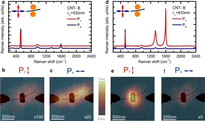
In the following, we characterize the intrinsic Raman response of CNT-B with an excitation wavelength of 532 nm, where no enhancement from the dimer occurs. The observed Raman features obey the characteristics outlined in the previous paragraphs. They serve as a reference to discuss plasmonic enhancement from a qualitative and quantitative point of view. Figure 4a shows the Raman spectra of CNT-B for Py (red) and Px (blue). Both spectra show the typical nanotube G-mode feature at 1590 cm–1. The absence of radial breathing modes indicates that none of the single-walled carbon nanotubes forming CNT-B is resonantly excited very close to its optical transition. The Raman intensity for Px, parallel to the nanotube axis, dominates the spectra. The G-peak intensity ratio G(Py)/G(Px) ≈ 0.15 based on integrated peak areas is a characteristic feature for Raman scattering of carbon nanotubes as discussed in the previous paragraph. At the dimer location the CNT-B is rotated around 75° away from the y-axis of our laboratory frame. Therefore, the experimentally observed ratio G(Py)/G(Px) represents a lower limit of the anisotropy (and an upper limit of the ratio) in light scattering by this tube, which will become important at a later stage.
Figure 4.
(a) Raman spectra of CNT-B for an excitation of 532 nm for Py (red) and Px (blue). Corresponding Raman maps of the integrated G-peak intensity are depicted in (b) and (c), respectively. (d) Raman spectra for an excitation of 638 nm for Py (red) and Px (blue). Corresponding Raman maps of the integrated G-peak intensity are shown in (e) and (f), respectively. A scaling factor relative to the map in (e) is given within the panels.
Raman maps of the G-peak intensities are shown in Figure 4(b, Py) and (c, Px). For all maps in this work, the intensity is normalized to the Si peak at 521 cm–1. The Raman maps are overlaid with AFM data to correlate the Raman intensity with the tube position. The intensities vary (i) as a function of the overlap between CNT-B and the laser spot as well as (ii) the relative orientation of the corresponding CNT-segment and the laser polarization. To the left of the dimers, for instance, the G-peak intensity for Py almost vanishes. For Px, all segments of CNT-B show a considerable Raman intensity.
Once the plasmonic enhancement comes into play, we observe drastic changes in the Raman signatures of CNT-B with respect to intensity, polarization behavior and spatial distribution. Figure 4d shows the Raman spectra for Py (red) and Px (blue), excited at the plasmonic resonance of the dimer structure. CNT-B is now subject to plasmonic enhancement. The intensity is much stronger compared to the off resonant case in Figure 4a. The Raman intensity for Py dominates the spectra and provides a clear evidence for plasmonic enhancement due to the strong near-field located in the cavity. The intensity ratio in the plasmon-enhanced Raman spectra is G(Py)/G(Px) ≈ 30. The ratio is inverted compared to the standard Raman process (0.15). The inversion is a sign of the enhancement by localized surface plasmons. Further evidence for cavity induced enhancement for Py is provided by the Raman map of the integrated G-mode intensity shown in Figure 4e. The signal exclusively arises from nanotube segments within the cavity.
Interestingly, we observe a signal localization also for Px, as shown in Figure 4f. The signal is considerably weaker than for Py, but occurs mainly in the vicinity of the dimer. This is in stark contrast to the spatial distribution of the Raman signal for Px upon excitation with 532 nm in (c). The lack of signal for Px away from the dimers may be due to the fact that CNT-B contains a nanotube segment resonant at 633 nm only close to the cavity. We discard this interpretation in light of the homogeneous intensity distribution for 532 nm in Figure 4b. Instead, minor plasmonic enhancement may also occur for Px where the near-field predominantly extends along the horizontal axis for both dimers, see Figure 3d. We recently observed this behavior for comparable dimer structures covered with graphene.22 For 633 nm, we observe a considerable defect-induced D-mode at around 1330 cm–1 for both polarizations, consistent with the characterization of the CNT starting material, see Supporting Information S4.
In the following, we deduce the overall plasmonic enhancement via intensity, polarization behavior, and signal localization when the cavity is switched “on” and “off”. Comparing the experimentally observed intensity ratios G(Py)/G(Px) in the presence (∼30 at 633 nm) and absence (∼0.15 at 532 nm) of plasmonic enhancement, we arrive at an enhancement factor of ∼200. Note that this represents a lower bound, as we treat the signal observed for Px at 633 nm as if it were the intrinsic response of CNT-B. In addition, G(Py)/G(Px) ≈ 0.15 for 532 nm represents an upper bound as previously discussed. The enhancement increases further if we take into account the localization of the signal in the cavity. A line profile of the integrated G-peak intensities extracted from Figure 4e shows that the signal is localized to within 440 nm around the dimer (full width at half-maximum, see Supporting Information S4). It represents the convolution of the laser spot with the enhanced signal arising from the cavity. By comparing the size of the laser spot ≈ 880 nm with the width of the cavity (∼100 nm) we arrive at an overall enhancement factor of 1.8 × 10³.
The inverted polarization behavior, Figure 4d, raises the question whether the Raman process in the presence of strong near-fields requires going beyond the conventional framework of Raman scattering in carbon nanotubes. Does the high intensity near-field bring out E1(g)- and E2(g)-type phonons that are allowed for incident light polarized perpendicular to the nanotubes axis? These vibrations are expected as additional features of the G-peak. Figure 5 compares the G-peak spectra extracted from Figure 4 scaled to a comparable intensity. The corresponding polarizations and the state of the cavity enhancement (on/off) is schematically depicted next to each spectrum. The intrinsic G-peak (green trace) is neither affected by the polarization of the incident light (red) nor the presence of enhancing near-fields (blue and red). Without enhancement (λ = 532 nm, G(Px)), the G-peak consists of A1(g)-type phonons. Therefore we conclude that the Raman signal of CNT-B arising from enhanced near-fields polarized perpendicular the nanotube axis is dominated by A1(g)-type vibrations as well. No indication of E1(g)- and E2(g)-type phonons is found.
Figure 5.
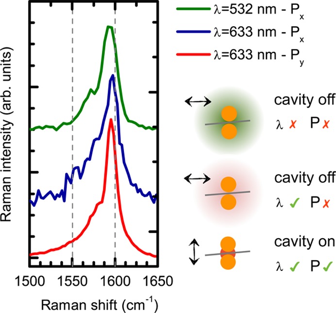
G-peak shape of CNT-B without plasmonic enhancement (green, blue) and plasmonic enhancement in the cavity switched on (red). The spectra are scaled to equal intensities to compare the peak shape. The state of the cavity is schematically broken down into the corresponding polarization and excitation wavelength of the incident light.
Takase et al.34 investigated plasmon-enhanced Raman scattering of carbon nanotubes randomly dispersed on top of closely spaced plasmonic nanodimers. The authors assigned features in their G-peak spectra to E1(g) and E2(g) type phonons associated with polarizations perpendicular to the nanotubes axis and postulated a breakdown of electronic transition selection rules under plasmonic enhancement. We note that ref (34) presented no data to confirm the presence of isolated, individual tubes in the plasmonic hotspots. Their Raman data can alternatively be explained as A1(g) phonons arising from different nanotubes. This straightforward explanation requires no activation of normally surpressed Raman modes in nanotubes or a breakdown of the (robust) selection rules for optical transitions.
In the following, further evidence for the conventional nature of plasmon-induced Raman scattering in carbon nanotubes is provided. We compare CNT-B to another carbon nanotube bundle (CNT-R) placed in a comparable cavity. Its experimental features are given in the Supporting Information S4. While CNT-B is oriented at around 75° with respect to the dimer axis, CNT-R is oriented almost perpendicular to it. Applying a similar analysis as above, the enhancement factor for CNT-R drops by at least a factor of ∼20. We explain the difference in the enhancement factors by the orientation of the nanotube bundles within the cavity. For CNT-R, the polarization of the near-field is polarized entirely perpendicular to the nanotube axis. Even though the near-field is strong, it is largely screened by the nanotube and the signal intensity is low. For CNT-B, in contrast the near-field in the cavity is partially projected on the nanotube axis without being screened by surface charges, leading to increased experimental signal intensities. A similar projection mechanism occurs in tip enhanced Raman scattering of carbon nanotubes and supports our interpretation.35
The dimer cavities are expected to yield an enhancement of the order of 104, see Supporting Information S3. The partial or vanishing projection of the near-field polarization onto the nanotubes’ axis translates into lower enhancement factors that we observe for CNT-B (103) and CNT-R (102). This orientation dependence emphasizes the flexibility of our nanotube–nanoplasmonic interface. To address phenomena where an optical excitation perpendicular to the nanotube is required, configurations like CNT-R should be realized. For maximal signal enhancement, for example, to combine Raman measurements with electrical transport, the antenna structure should be rotated by, for example, 15° against the electrode axis to allow a projection of the near-field polarization on the nanotube axis as it is the case for CNT-B.
Our assembly scheme will allow to independently tune the optical properties of the two components forming the nanotube–nanoplasmonic interface. Single-chirality carbon nanotube device arrays were successfully assembled by DEP,19 thereby providing tubes with defined and uniform optical resonances. On the other hand, the localized surface plasmon resonance of the plasmonic nanostructures can be tuned by varying the size of the nanodisks and the gap, and by using alternative cavity designs such as bow tie antennas. Ideally, a nanotube crosses the cavity and connects electrodes, such as CNT-R. As a proof of principle, current versus voltage characteristics of a nanotube connecting two electrodes but without a plasmonic structure are presented in the Supporting Information S5. In this case, the floating electrode is addressed via conductive AFM. A connected carbon nanotube will serve as a near-field probe whose characteristics upon illumination can be accessed electrically. Alternatively, the CNT may act as a nanoscale light emitter in the cavity via electroluminescence36 or phonon-assisted electroluminescence.37 It serves as an emissive dipole of known position and orientation, which is independent of selection rules present if an optical excitation triggers light emission.
In summary, we assembled nanoplasmonic–nanotube interfaces by the directed dielectrophoretic deposition of carbon nanotubes on top of plasmonic antennas. For nanotubes in a plasmonic cavity, we probed with plasmon-enhanced Raman scattering optical coupling in the nanoscale. We observed plasmonic enhancement on the order of 103, which exclusively arises from carbon nanotube segments inside the cavity. The enhanced Raman signal arose from fully symmetric vibrations and was treated within the conventional framework of Raman selection rules in carbon nanotubes. Highly enhanced near-fields do not translate directly into enhanced Raman signals but depend on the orientation of a carbon nanotube inside the cavity. Beyond basic research, the scalability of our assembly scheme qualifies nanotube–nanoplasmonic systems as an excellent candidate to increase the performance of carbon nanotubes as highly sensitive photodetectors and efficient light-harvesters.
Method Summary
Fabrication
Sets of plasmonic structures, placed in between electrode pairs with a gap of 1 μm, were exposed by electron-beam lithography in a LEO 1530 Gemini FEG SEM and a Raith Elphy Plus Lithography System with Laser Interferometer Stage. Metallization was carried out by evaporating 5 nm Cr + 40 nm Au followed by lift-off in an ultrasonic bath. Each set consisted of 90 electrode pairs, 45 of which contained plasmonic structures.
Dielectrophoresis
Ultrapure, unsorted SWCNTs (http://www.nanointegris.com) in an aqueous surfactant solution were used in this work. A dilution of 4 × 10⁻⁴ mg/mL was prepared and a droplet of 0.5 μL was placed on top of the substrate. An ac electric field of 6 Vpp at a frequency of 200 kHz was generated by a TG1010 programmable 10 MHz function generator. A Karl Suss probe station with tungsten probes was used to connect the electrodes array with the function generator in order to accurately position the SWCNTs at the desired sites by dielectrophoresis. After 1 min, DI water was used to rinse the substrate and a gentle stream of N2 was used to dry it.
Structural Characterization
The nanostructures were characterized before and after CNT deposition using a Veeco Dimension 3100 AFM, a Park Systems XE 150 AFM and an XL30 Sirion FEI FEG SEM.
Dark-Field Spectroscopy
The sample was illuminated by a polarized white light from a halogen bulb. A 50×, NA 0.55, IR-corrected microscope objective was used to collect the scattered light that is directed to a spectrometer that is equipped with a CCD detector to obtain the spectra in the visible range. The spectra were acquired at isolated plasmonic structures outside the electrode array to avoid contributions from the electrode tips.
Simulations
We simulated a gold dimer (disk diameter 100 nm, height 40 nm, and separation 24 nm), compare Figure 2, on top of a 5 nm Cr adhesion layer on a 300 nm SiO2/Si substrate. For our numerical calculations, three-dimensional (3D) simulations were performed to calculate the scattering cross sections (not shown) and the near-field enhancement of the coupled nanostructures by using a commercially available finite-difference-timedomain code (Lumerical FDTD). The dielectric functions of Au used in the simulations were extracted from data by Johnson and Christy.38 The Cr adhesion layer and the SiO2 layer were included in the simulations. The near-field distributions were evaluated for an excitation of 633 nm.
Raman Spectroscopy
Raman spectra were obtained with a WiTec single-grating spectrometer using a 100× objective with integration times between 1 and 30 s. The laser power on the sample was kept below 0.5 mW. To change the polarization, we rotate the sample by 90° while all other experimental parameters are left unchanged. Spatial Raman scans were performed using a piezo stage with a stepsize of 50 nm. The Raman spectra were calibrated using a neon lamp.
Acknowledgments
The authors thank B. Hatting and R. Krupke for fruitful discussions, F. Schedin for help with sample fabrication, N. Clark for help in figure preparation, and C. Casiraghi for use of equipment. S.H., C.L., and S.R. acknowledge funding by German Research Foundation (DFG via SFB 658, subproject A6; DFG via EraNet, Nanospec, 566322), the ERC (Grant 210642), and the NanoScale Focus Area. R.F.G. and S.A.M. acknowledge funding by the Leverhulme Trust (U.K.) and the U.K. Engineering and Physical Sciences Research Council (EPSRC). A.O. and A.V. acknowledge the Engineering and Physical Science Research Council (EPSRC) U.K. (Grant EP/G035954/1).
Supporting Information Available
Dielectrophoretic deposition of CNTs and yields; near-field simulations; phonon symmetries and selection rules; fully symmetric vibrations, their Raman tensor, and angle-dependent Raman intensities; Raman intensity of CNT-B; Raman spectra of CNT starting material; G-mode comparison of the starting material and CNT-B; width of laser spot from Raman line scan; characterization of CNT-R; additional CNTs interfaced with dimer structures showing enhancement; and conductive AFM. This material is available free of charge via the Internet at http://pubs.acs.org.
The authors declare no competing financial interest.
Supplementary Material
References
- Bachelier G.; Butet J.; Russier-Antoine I.; Jonin C.; Benichou E.; Brevet P.-F. Phys. Rev. B 2010, 82, 235403. [DOI] [PubMed] [Google Scholar]
- Walsh G. F.; Dal Negro L. Nano Lett. 2013, 13, 3111–3117. [DOI] [PubMed] [Google Scholar]
- Barnes W. L.; Dereux A.; Ebbesen T. W. Nature 2003, 424, 824–830. [DOI] [PubMed] [Google Scholar]
- Maier S. A.; Atwater H. A. J. Appl. Phys. 2005, 98, 011101. [Google Scholar]
- Stewart M. E.; Anderton C. R.; Thompson L. B.; Maria J.; Gray S. K.; Rogers J. A.; Nuzzo R. G. Chem. Rev. 2008, 108, 494–521. [DOI] [PubMed] [Google Scholar]
- Kneipp K.; Kneipp H.; Bohr H. G.. Surface-Enhanced Raman Scattering: Physics and Applications; Springer Verlag: Berlin, 2006/2007; pp 261–277. [Google Scholar]
- Maier S. A. Opt. Express 2006, 14, 1957–1964. [DOI] [PubMed] [Google Scholar]
- Maier S. A.Plasmonics: Fundamentals and Applications; Springer: Berlin, 2007. [Google Scholar]
- Fleischmann M.; Hendra P. J.; McQuillan A. J. J. Photochem. Photobiol. A 1974, 26, 163–166. [Google Scholar]
- Jeanmaire D. L.; Van Duyne R. P. J. Electroanal. Chem. 1977, 84, 1–20. [Google Scholar]
- Nie S. Science 1997, 275, 1102–1106. [DOI] [PubMed] [Google Scholar]
- Kneipp K.; Wang Y.; Kneipp H.; Perelman L.; Itzkan I.; Dasari R.; Feld M. Phys. Rev. Lett. 1997, 78, 1667–1670. [Google Scholar]
- Le Ru E. C.; Etchegoin P. G. Annu. Rev. Phys. Chem. 2012, 63, 65–87. [DOI] [PubMed] [Google Scholar]
- Chu H.; Wang J.; Ding L.; Yuan D.; Zhang Y.; Liu J.; Li Y. J. Am. Chem. Soc. 2009, 131, 14310–14316. [DOI] [PubMed] [Google Scholar]
- Assmus T.; Balasubramanian K.; Burghard M.; Kern K.; Scolari M.; Fu N.; Myalitsin A.; Mews A. Appl. Phys. Lett. 2007, 90, 173109. [Google Scholar]
- Ilani S.; McEuen P. L. Annu. Rev. Condens. Matter Phys. 2010, 1, 1–25. [Google Scholar]
- Krupke R.; Hennrich F.; Weber H. B.; Kappes M. M.; von Löhneysen H. Nano Lett. 2003, 3, 1019–1023. [Google Scholar]
- Vijayaraghavan A.; Blatt S.; Weissenberger D.; Oron-Carl M.; Hennrich F.; Gerthsen D.; Hahn H.; Krupke R. Nano Lett. 2007, 7, 1556–1560. [DOI] [PubMed] [Google Scholar]
- Vijayaraghavan A.; Hennrich F.; Stürzl N.; Engel M.; Ganzhorn M.; Oron-Carl M.; Marquardt C. W.; Dehm S.; Lebedkin S.; Kappes M. M.; Krupke R. ACS Nano 2010, 4, 2748–2754. [DOI] [PubMed] [Google Scholar]
- Jain P. K.; El-Sayed M. A. Chem. Phys. Lett. 2010, 487, 153–164. [Google Scholar]
- Alonso-González P.; Albella P.; Neubrech F.; Huck C.; Chen J.; Golmar F.; Casanova F.; Hueso L. E.; Pucci A.; Aizpurua J.; Hillenbrand R. Phys. Rev. Lett. 2013, 110, 203902. [DOI] [PubMed] [Google Scholar]
- Heeg S.; Fernández-Garca R.; Oikonomou A.; Schedin F.; Narula R.; Maier S. A.; Vijayaraghavan A.; Reich S. Nano Lett. 2013, 13, 301–308. [DOI] [PubMed] [Google Scholar]
- Ajiki H.; Ando T. Physica B 1994, 201, 349–352. [Google Scholar]
- Benedict L. X.; Louie S. G.; Cohen M. L. Phys. Rev. B 1995, 52, 8541–8549. [DOI] [PubMed] [Google Scholar]
- Tasaki S.; Yamabe T. Phys. Rev. B 1998, 57, 9301–9318. [Google Scholar]
- Tang Z. K.; Wang N.; Li G. D.; Chen J. S. Nature 2000, 408, 50–51. [DOI] [PubMed] [Google Scholar]
- Thomsen C.; Reich S. In Light Scattering in Solid IX: Novel Materials and Techniques; Topics in Applied Physics; Cardona M., Ed.; Springer Verlag: Berlin, 2007; Vol. 108, pp 115–235. [Google Scholar]
- Duesberg G.; Loa I.; Burghard M.; Syassen K.; Roth S. Phys. Rev. Lett. 2000, 85, 5436–5439. [DOI] [PubMed] [Google Scholar]
- Telg H.; Maultzsch J.; Reich S.; Hennrich F.; Thomsen C. Phys. Rev. Lett. 2004, 93, 177401. [DOI] [PubMed] [Google Scholar]
- Maultzsch J.; Telg H.; Reich S.; Thomsen C. Phys. Rev. B 2005, 72, 205438. [DOI] [PubMed] [Google Scholar]
- Jorio A.; Saito R.; Hafner J.; Lieber C.; Hunter M.; McClure T.; Dresselhaus G.; Dresselhaus M. Phys. Rev. Lett. 2001, 86, 1118–1121. [DOI] [PubMed] [Google Scholar]
- Fantini C.; Jorio A.; Souza M.; Strano M.; Dresselhaus M.; Pimenta M. Phys. Rev. Lett. 2004, 93, 147406. [DOI] [PubMed] [Google Scholar]
- Duque J. G.; Chen H.; Swan A. K.; Shreve A. P.; Kilina S.; Tretiak S.; Tu X.; Zheng M.; Doorn S. K. ACS Nano 2011, 5, 5233–5241. [DOI] [PubMed] [Google Scholar]
- Takase M.; Ajiki H.; Mizumoto Y.; Komeda K.; Nara M.; Nabika H.; Yasuda S.; Ishihara H.; Murakoshi K. Nat. Photonics 2013, 7, 550–554. [Google Scholar]
- Cançado L. G.; Jorio A.; Ismach A.; Joselevich E.; Hartschuh A.; Novotny L. Phys. Rev. Lett. 2009, 103, 186101. [DOI] [PubMed] [Google Scholar]
- Mueller T.; Kinoshita M.; Steiner M.; Perebeinos V.; Bol A. A.; Farmer D. B.; Avouris P. Nat. Nanotechnol. 2009, 5, 27–31. [DOI] [PubMed] [Google Scholar]
- Essig S.; et al. Nano Lett. 2010, 10, 1589–1594. [DOI] [PubMed] [Google Scholar]
- Johnson P. B.; Christy R. W. Phys. Rev. B 1972, 6, 4370–4379. [Google Scholar]
Associated Data
This section collects any data citations, data availability statements, or supplementary materials included in this article.


