Abstract
In this paper, we present and demonstrate RF-MEMS load sensors designed and fabricated in a suspended architecture that increases their quality-factor (Q-factor), accompanied with an increased resonance frequency shift under load. The suspended architecture is obtained by removing silicon under the sensor. We compare two sensors that consist of 195 μm × 195 μm resonators, where all of the resonator features are of equal dimensions, but one’s substrate is partially removed (suspended architecture) and the other’s is not (planar architecture). The single suspended device has a resonance of 15.18 GHz with 102.06 Q-factor whereas the single planar device has the resonance at 15.01 GHz and an associated Q-factor of 93.81. For the single planar device, we measured a resonance frequency shift of 430 MHz with 3920 N of applied load, while we achieved a 780 MHz frequency shift in the single suspended device. In the planar triplet configuration (with three devices placed side by side on the same chip, with the two outmost ones serving as the receiver and the transmitter), we observed a 220 MHz frequency shift with 3920 N of applied load while we obtained a 340 MHz frequency shift in the suspended triplet device with 3920 N load applied. Thus, the single planar device exhibited a sensitivity level of 0.1097 MHz/N while the single suspended device led to an improved sensitivity of 0.1990 MHz/N. Similarly, with the planar triplet device having a sensitivity of 0.0561 MHz/N, the suspended triplet device yielded an enhanced sensitivity of 0.0867 MHz/N.
Keywords: Fabrication, IC, resonance frequency shift, quality-factor, bio-implant, RF-MEMS
1. Introduction
In the case of major fractures in humans, fixation plates are commonly implanted to facilitate bony healing. When the plate is implanted, it assumes a majority of the load and demonstrates a relatively high associated strain. During the course of healing, the tissue consolidates and the strain in the plates decreases. The strain change profile over time can be found in [1]. To monitor the healing process, a bio-implantable sensor is needed to observe the strain change in real-time. For this purpose, we present RF-MEMS resonator sensors that shift their resonance frequency when an external force is applied and strain occurs. The structure of these sensors is based on spiral RF coil architecture that provides a distributed LC tank circuit. The operating principle of these sensors relies on the resonance frequency shift as a result of the dielectric area (and thus the film capacitance between the metal and the substrate) changing with the externally applied load. Therefore, using these RF-MEMS load sensors, the induced strain can in principle be monitored in real-time to observe the fracture healing process by tracking the shift of resonance frequency. While there are also some other bio-sensor reports in the literature [2–6], our sensors are unique in that they monitor the strain wireless and with small dimensions.
Previously, we developed on-chip resonators [7, 8]. In [7], the highest Q-factor with the smallest size at high frequency (15 GHz) was demonstrated. We also showed proof-of-concept of resonator-based sensors in [9]. In this work, we propose and demonstrate RF-MEMS load sensors designed and fabricated in a suspended architecture to achieve a higher shift in resonance frequency and an enhanced level of Q-factor and sensitivity compared to the previous resonators.
In this paper, we introduce the effects of suspended architecture on a resonator for RF MEMS bio-implant sensors, which rely on resonance frequency shift to monitor fracture healing. Using a silicon substrate to fabricate our chips, we describe the suspended architecture obtained by etching the silicon though a carefully designed mask. This new design, which is obtained by partially removing the substrate of the single planar device, is called the single suspended device. Applying load to both of these devices (planar vs. suspended), we observed their resonance frequencies, change in their resonance frequencies, and their Q-factors. We found a higher Q-factor for the single suspended device compared to single planar device. Further, the single suspended device led to a higher resonance frequency (f0) shift compared to the single planar device. We also achieved a higher f0 shift compared to our previously published data in [9] as a result of partially etching the substrate. The rest of the paper presents our theoretical background and design process, fabrication processes, and experimental characterization and analysis sections.
2. Theoretical Background and Design
Our aim is to design bio-compatible sensors with maximum Q-factor and maximum resonance frequency shifts. By using the circuit model in [8], the formulas in [7, 8], and techniques available in the literature [10–18], we design our devices to maximize the Q-factor. The formulas in [9, 19] are used during device design process to have maximum frequency shift. We use gold as the metal layer, Si3N4 as the dielectric and silicon (identical to the ones used in [7]) as the substrate so that our chip is fully bio-compatible and has a high Q-factor. To obtain a high Q-factor with minimum spacing, our technique leverages the film capacitance (Cfilm) as the main capacitance change in the LC tank circuit with the spiral geometry, as in [7, 8]. In order to obtain a high Q-factor, dielectric, dielectric thickness, effects of substrate, metal layer, metal layer thickness, metal layer width, spacing, number of turns and area should also be considered carefully. The other important aspect of the design is the resonance frequency shift. The main driver of the resonance frequency shift is the change in the area of the dielectric, and, as a result, the change in the value of the capacitance. When the load is applied, since the Young’s modulus of silicon and gold is high, the main change occurs in the dielectric area as verified by the Coventorware simulation, which is described in detail in [9].
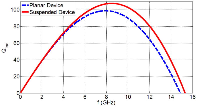
The parameters of the single planar device are presented in Table I. We remove the substrate of another chip, with all the same parameters, to obtain the single suspended device. By using this technique, we theorize that higher Q-factors and shifts of resonance frequency will result. When we etch the substrate, we decrease the substrate loss. As a result, we increase the silicon resistance (Rsi) and decrease the silicon capacitance (Csi). Hence, the overall result is an increase in the parallel resistance (RP). By engineering a higher substrate loss factor, a higher inductor quality-factor (Qind) and hence a higher Q-factor of the device are obtainable, as explained in details in [7, 8]. The resonator quality factor (Q) is obtained from the inductor quality factor (Qind) and capacitor quality factor (Qc) as given in [8] by: From this relation, it is possible to observe that increasing the inductor quality-factor will increase the resonator quality factor. Due to the higher Rsi and lower Csi, we have a lower parallel capacitance (Cp); therefore, a higher self resonance factor is obtained at the same frequency compared to the case with single planar device. Thus, the resonance frequency is also higher. Combining all these effects, we obtain higher Q-factors and higher resonance frequencies with silicon removal. Figure 1 presents the Qind-factors of the single suspended device and the single planar device.
Table I.
The Parameters of The Resonator Device.
| Lc(μm) | Wc (μm) | N | w (μm) | s (μm) | tox (μm) | t (μm) |
|---|---|---|---|---|---|---|
| 195 | 195 | 2 | 35 | 5 | 0.1 | 0.1 |
Fig. 1.
The Qind of the singular devices with respect to frequency.
By etching the substrate, we will also have higher shift of resonance frequency. This can be examined from two aspects. As a result of the etching of the substrate, the strain propagation will be higher. Since the strain first occurs in the substrate then pass to the dielectric and metal layers, with an etched substrate, there will be more strain and as a result, there will be more capacitance change. Hence, there will be a higher f0 shift. If we apply the same load to the single planar device and the single suspended device, assuming they have the same resonance frequency, we will have higher shift of resonance frequency (Δf0) in the single suspended device as a result of higher strain in dielectric and metal layer. Secondly, if we have two chips with same relative shift ( ), the chip with the higher f0 will have the higher Δf0 as well. Thus the chip with etched substrate, with its higher f0, also has a higher Δf0. If we combine these two rationales, we expect to have a higher Δf0 in the chip with the etched substrate. Also, due to the strain amplification effect we also expect that the silicon-etched chip has a higher sensitivity ( ). Considering all these factors, we postulate that the suspended architecture yields a higher f0 shift and higher sensitivity.
3. Fabrication
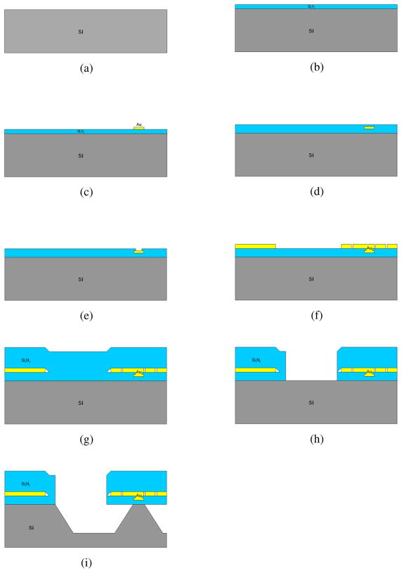
Figure 2 provides a detailed schematic view of our fabrication procedure. We use an n-type 500 μm thick substrate with a <100> orientation. We deposit a Si3N4 thin film using a plasma-enhanced chemical vapor deposition (PECVD) system; this film is 0.1 μm thick (Fig. 2b). We then lay down the first metal layer (contact layer) made of Au with a thickness of 0.1 μm (Fig. 2c). A 0.1 μm thick Si3N4 thin film is subsequently deposited (Fig. 2d). This film is patterned and vertical interconnection areas are opened using a wet etching process with HF (Fig. 2e). We also perform an Au (gold) metallization step to make the interconnects and top coil construction (Fig. 2f). A 0.8 μm thick Si3N4 film is deposited (Fig. 2g) and this layer is patterned and etched by HF (Fig. 2h). Finally, using potassium hydroxide (KOH), we partially etch the silicon as shown in Fig. 2i.
Fig. 2.
The Fabrication Procedure.
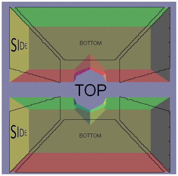
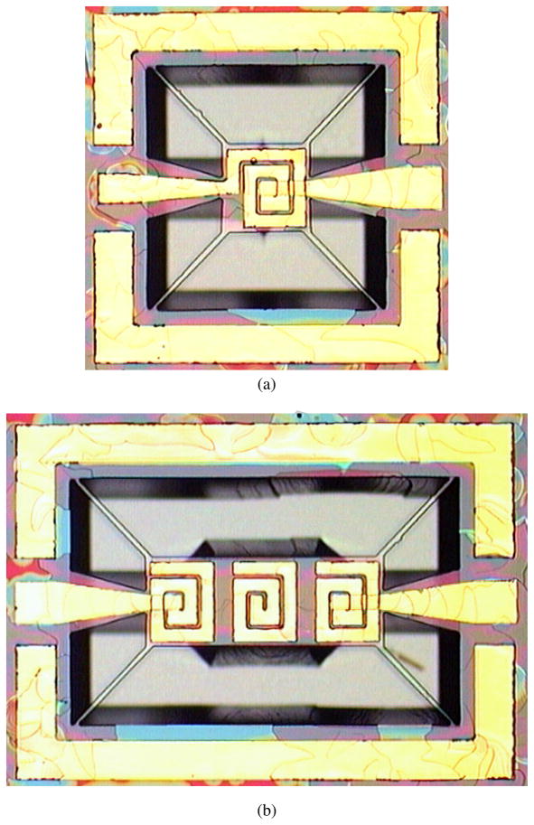
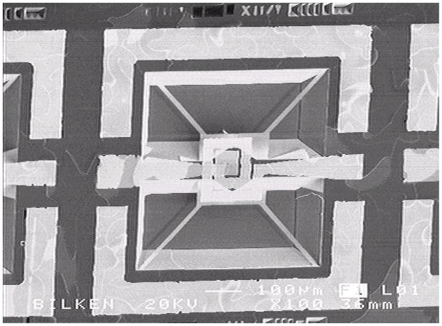
Unlike other process flows used in [7–9], here we initially put down the Si3N4 thin film to protect the contact metal layer while silicon is being etched. Since KOH also etches the metal layer, we use the first and third Si3N4 layers as etch-stop layers. The second Si3N4 layer acts as our dielectric layer. For silicon etching, we use a process simulation (ACES), with its simulation results shown in Fig. 3. Using a KOH solution with a concentration of 30 percent at 65°C gives an etch rate of 1.1 μm/min, as expected from our chemical kinetics simulation. Thus, after 70 minutes, a depth of 77 μm is etched. This is the maximum feasible etch depth that avoids damaging the device given the architecture and size of the sensor. Since etching the substrate deep enough increases the Q-factor and sensitivity, we used the maximum feasible etching to obtain the best possible performance for this sensor geometry in practice. Here it is worth noting that, although etching helps especially at the beginning, etching has a diminishing effect in improving the Q-factor and sensitivity after a certain point. In our case, this etch depth of 77 μm is practically good enough for a proof-of-concept demonstration of the resulting improvements. The final structures are visualized in Fig. 4 and the associated SEM image of the single suspended device is presented in Fig. 5.
Fig. 3.
Simulation of the Silicon Etching. The trapezoids represent areas where there are no Si3N4. KOH solution etches the silicon through these regions.
Fig. 4.
Planar images of the devices: a) the fabricated single suspended device and b) the fabricated suspended triplet device.
Fig. 5.
SEM image of the single suspended device.
4. Experimental Characterization and Analysis
We characterize our resonator sensors with a custom-design apparatus; details of the setup can be found in [9]. We first measure S21 parameters of our devices by the network analyzer when there is no load. The S21 parameters are also then recorded when applying loads of 1960, 2940 and 3920 N (i.e., 200, 300 and 400 kgf). Using this experimental protocol, the resonance frequencies (f0), Q-factors, and f0 shifts are determined under different levels of applied loads. In our characterization, we apply up to 400 kgf (3920 N) because the human body can effectively apply 4 times of its weight to a bone; for example, a human body with a weight of 100 kgf can generate a mechanical loading of 400 kgf for a bone. During operation, in one frequency scan of the network analyzer, there are only a limited number of data points; it is thus easier to track smaller shifts in the transmission spectra in response to the applied load when the sensitivity is higher. Therefore, higher sensitivity, which results in larger shifts in transmission with the same level of induced strain, is highly preferred to read out the strain correctly. In this work, we characterized the single suspended device, the single planar device, the suspended triplet device and the planar triplet device to compare their performances with respect to each other including their resonance frequencies, Q-factors, and sensitivities. Here with the “triplet” configuration, we refer to a method of characterizing the sensor on the chip telemetrically where all the receiver and transmitter antennas are placed on the same chip side by side with the sensor; further details can also be found in [9].
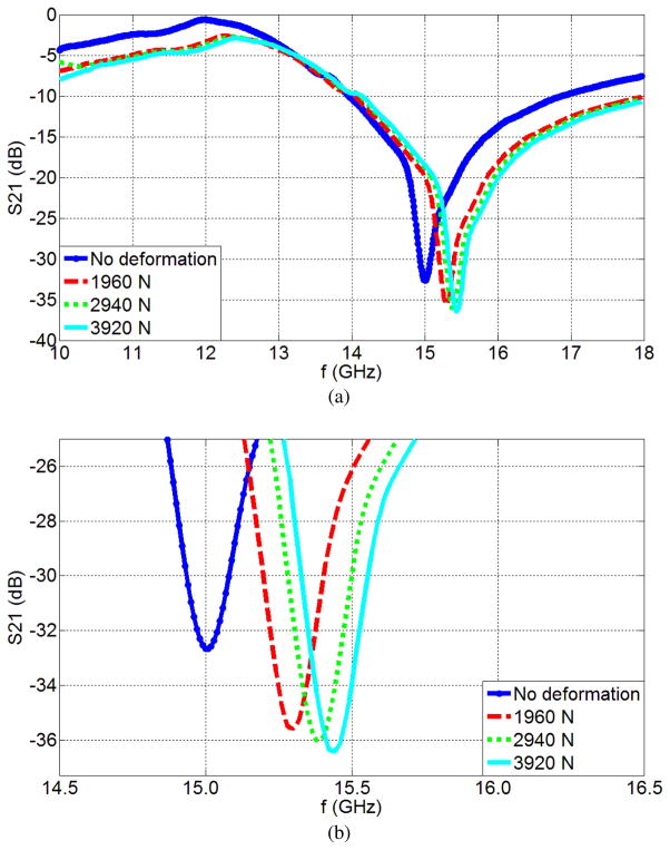
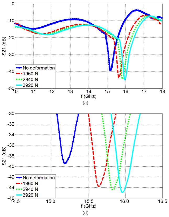
Figure 6 shows the S21 parameters of the single suspended device and the single planar device under different applied load values. Figure 6a gives the S21 parameters of the single planar device under different loads and Figure 6b, provides a magnified view of this information. The S21 parameters of the single suspended device under different applied loads are shown in Figures 6c and 6d. There is a considerable increase of the resonance frequency for single suspended devices.
Fig. 6.
Experimental measurements of the S21 parameters as a function of frequency for: (a) the Single Planar Device and (b) zoom in for the Single Planar Device, (c) the Single Suspended Device and (d) zoom in for the Single Suspended Device. Data is presented for the cases of no deformation and also when loads of 1960 N, 2940 N and 3920 N are applied.
Table II displays the resonance frequencies of the single planar devices under different loads. The single planar device has a resonance frequency of 15.01 GHz under no deformation and demonstrates 430 MHz shift with 3920 N applied.
Table II.
Resonance Frequencies of the Device Variants with Different Loads.
| Load | No load | 1960 N | 2940 N | 3920 N |
|---|---|---|---|---|
| Single Planar Device | 15.01 GHz | 15.30 GHz | 15.39 GHz | 15.44 GHz |
| Single Suspended Device | 15.18 GHz | 15.64 GHz | 15.83 GHz | 15.96 GHz |
| Planar Triplet | 15.06 GHz | 15.17 GHz | 15.23 GHz | 15.28 GHz |
| Suspended Triplet | 15.41 GHz | 15.56 GHz | 15.66 GHz | 15.75 GHz |
For the single suspended device, it demonstrates a 15.18 GHz resonance frequency with no deformation (Table II). Its resonance frequency increases 780 MHz with 3920 N applied load. There is an increase in resonance frequency for the single suspended device compared to single planar device with no load, as expected and hypothesized in the theoretical background and design section. The table also shows a significant increase in the resonance frequency shift in the single suspended device compared to the single planar device.
Table II shows the increase in resonance frequency with applied load. The underlying reason is that, under load, the dielectric area decreases and the capacitance decreases. Hence, there is a concomitant resonance frequency increase. In addition, since the relation between the capacitance change and resonance frequency is nonlinear, then the resonance frequency shift is nonlinear.
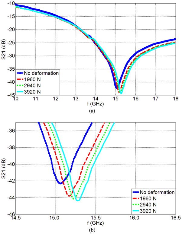
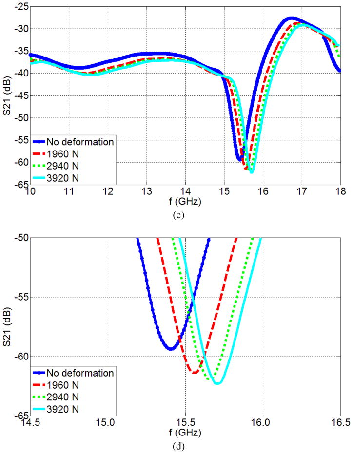
For the triplet case, we can see the S21 parameters of the suspended triplet device and the planar triplet device under different applied loads in Fig. 7. The figures display a considerable increase of the resonance frequency for suspended triplet devices compared to the planar triplet devices. If we observe the resonance frequencies for triplet cases, we will see that the planar triplet device has a resonance frequency of 15.06 GHz with no deformation, and the suspended triplet device displays 15.41 GHz with no deformation (Table II). The resonance frequency shift of the planar triplet device is 220 MHz under 3920 N load while the resonance frequency shift of the suspended triplet device is 340 MHz under 3920 N load. In all cases of single and triplet devices, we measured each device 5 times. The presented points of resonance frequency correspond to the averages of these points of all 5 measurements. In these measurements, we also observed that the difference between the maximum and the minimum measured f0 (variable range of f0) is 0.02 GHz while their standard deviation is only ~0.01 GHz.
Fig. 7.
Experimental measurements of the S21 parameters as a function of frequency for: (a) the Planar Triplet Device and (b) zoom in for Planar Triplet Device, (c) the Suspended Triplet Device and (d) zoom in for Suspended Triplet Device. Data for the no deformation and also when loads of 1960 N, 2940 N and 3920 N are applied are presented.
Table III shows the device Q-factors that are obtained from Figures 6 and 7. We see that the single planar device has Q-factors of 93.81 under no load, and 111.08 under 3920 N load. The single suspended device yields an increase in Q-factor compared to the single planar device case. The single suspended device has Q-factors of 102.64 under no load, and 120.02 under 3920 N. The suspended triplet device has higher Q-factors compared to the planar triplet device case. The Q-factors of the planar triplet device are 51.90 when there is no load, and 62.55 when 3920 N load is applied. However, the Q-factors of the suspended triplet device are 67.15 with no load, and 80.45 when 3920 N load is applied. These data show that the Q-factor rises with the applied load, as expected from the load-related capacitance decrease.
Table III.
The Q-factors of the Variant Devices with Different Loads.
| Load | No load | 1960 N | 2940 N | 3920 N |
|---|---|---|---|---|
| Single Planar Device | 93.81 | 109.21 | 110.96 | 111.08 |
| Single Suspended Device | 102.06 | 116.54 | 119.47 | 120.02 |
| Planar Triplet | 51.90 | 57.38 | 60.82 | 62.55 |
| Suspended Triplet | 67.15 | 79.51 | 80.31 | 80.45 |
The sensitivity ( ) and relative shift ( ) are important parameters for a sensor. The sensitivity and relative shift of the sensors are presented in Table IV. We see that the single suspended device has higher sensitivity and relative shift compared to the single planar device case. The single planar device has a sensitivity of 0.1097 MHz/N while the single suspended device has a sensitivity of 0.1990 MHz/N. The single planar device has a 2.9% relative shift whereas the single suspended device has a 5.1% relative shift. The same comparison occurs for the triplet case, the suspended triplet device has both higher sensitivity and relative shift compared to the planar triplet device. The planar triplet device has a 0.0561 MHz/N sensitivity and a 1.5% relative shift while the suspended triplet device has a 0.0867 MHz/N sensitivity and a 2.2% relative shift. These data demonstrate that the single suspended device has a higher Q-factor compared to the single planar device presented in [7] and has a higher resonance frequency shift, higher sensitivity and higher relative shift compared to the case in [9].
Table IV.
The Sensitivities of the Variant Devices.
| Sensitivity | Relative Shift | |
|---|---|---|
| Single Planar Device | 0.1097 MHz/N | 2.9% |
| Single Suspended Device | 0.1990 MHz/N | 5.1% |
| Planar Triplet | 0.0561 MHz/N | 1.5% |
| Suspended Triplet | 0.0867 MHz/N | 2.2% |
If we compare the case of triplet and single devices, we observe that we have different experimental performance results in terms of signal level, resonance frequency, Q-factor and sensitivity. Since there is a distance between antennas on the chip, the signal level of the triplet device case is lower than that of the single device case. Besides, because of the interaction between antennas, the resonance frequency of the single device and triplet device is slightly different. Also in the single device case, the signal is directly fed to the device whereas in the triplet device case, it is sent via the external antennas on the same chip. As a result, the Q-factor of the triplet device is lower than that of the single device as expected. The shift of resonance frequency is observed to be lower in the case of triplet device compared to the single device case. The reason is that the external load is applied across a larger area in the triplet device, whereas it is applied to a smaller area in the single device case. Consequently, the shift of resonance frequency in the single device for the same level of external loading is higher compared to the triplet device, making its measured sensitivity to be higher in the single device case.
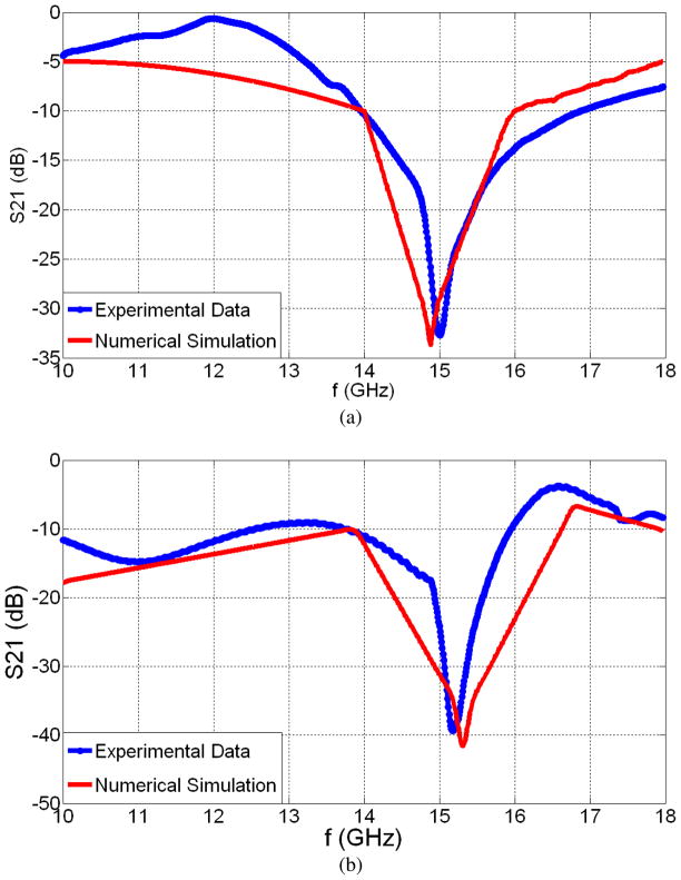
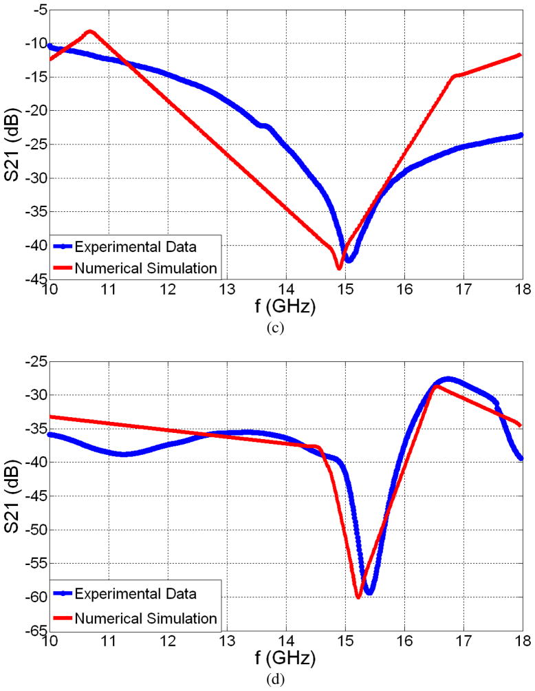
We also numerically simulate S parameters of our devices for the no-load case in CST Microwave Studio. The simulation results are given in Fig. 8. We observe generally good agreement between theoretical and experimental results from these figures. Table V gives the theoretical and experimental resonance frequencies and Q-factors in Table V. The single planar device theoretically has a 14.88 GHz resonance frequency and a 98.77 Q-factor (experimentally it demonstrates a 15.01GHz resonance frequency and 93.81 Q-factor). The single suspended device has a theoretical 15.31 GHz resonance frequency and a 117.41 Q-factor at the same time (experimentally it has a 15.18 GHz resonance frequency and 102.06 Q-factor). For triplet cases, we have a theoretical 14.9 GHz resonance frequency and a 57.62 Q-factor for the planar triplet device. The planar triplet device has a 15.06 GHz resonance frequency and a 51.90 Q-factor. For the suspended triplet device, we have a theoretical 15.22 GHz resonance frequency while the experimental resonance frequency is 15.41 GHz. The theoretical Q-factor for this device is 80.32 while the experimental one is 67.15. The theoretical and experimental resonance frequencies and Q-factors are observed to be reasonably close, but not identical. There is a slight difference between each pair of the simulated and measured values, which is attributed to the assumptions we make in our computations. In numerical simulations, we treat all components to be ‘ideal’; we assume perfect contact of the probes, perfect plane wave, perfect grounds, perfectly the same dimensions in design, and perfect environment with no external conditions affecting the signal or noise level. However, in real life, we experimentally face with all of these complications and measure all non-idealities in effect together, along with some degree of experimental error. Hence, the theoretical and experimental results differ slightly.
Fig. 8.
Numerical simulations for the S21 parameters when there is No Load (a) for the Single Planar Device, (b) for the Single Suspended Device, (c) for the Planar Triplet Device, and (d) for the Suspended Triplet Device.
Table V.
The Theoretical and Experimental Resonance Frequencies and Q-factors of the Variant Devices.
| f0 (GHz) | Q-Factor | |||
|---|---|---|---|---|
| Theoretical | Experimental | Theoretical | Experimental | |
| Single Planar Device | 14.88 GHz | 15.01 GHz | 98.77 | 93.81 |
| Single Suspended Device | 15.31 GHz | 15.18 GHz | 117.41 | 102.06 |
| Planar Triplet | 14.90 GHz | 15.06 GHz | 57.62 | 51.90 |
| Suspended Triplet | 15.22 GHz | 15.41 GHz | 80.32 | 67.15 |
5. Conclusion
In conclusion, we designed, numerically and analytically simulated, fabricated and experimentally characterized suspended RF-MEMS load sensors that achieve higher Q-factors and higher resonance frequency shifts compared to planar devices (devices without substrate etching). The single suspended device has a 102.06 Q-factor, a 780 MHz frequency shift, a 0.1990 MHz/N sensitivity and a 5.1% relative shift whereas the single planar device has a 93.81 Q-factor, 430 MHz frequency shift, they 0.1097 MHz/N sensitivity and a 2.9% relative shift. For triplet cases, the suspended triplet device has a 340 MHz frequency shift, a 0.0867 MHz/N sensitivity and a 2.2% relative shift while the planar triplet device has a 220 MHz frequency shift, a 0.0561 MHz/N sensitivity and a 1.5% relative shift. The suspended structures have greater resonance frequency shifts, sensitivities and relative shifts compared to all other cases presented heretofore. Therefore, the suspended architecture represents an improved geometry for monitoring strain in real-time. This improvement can be useful for the application of assessing the progression of healing osseous fractures.
Acknowledgments
This work is supported by the Turkish National Academy of Sciences Distinguished Young Scientist Award (TÜBA GEBİP), the European Science Foundation European Young Investigator Award (ESF-EURYI), and TÜBİTAK EEEAG 105E066, 105E065, 104E114, 106E020, 107E088, 107E297, and 109E004 and EU MOON 021391.
Footnotes
Publisher's Disclaimer: This is a PDF file of an unedited manuscript that has been accepted for publication. As a service to our customers we are providing this early version of the manuscript. The manuscript will undergo copyediting, typesetting, and review of the resulting proof before it is published in its final citable form. Please note that during the production process errors may be discovered which could affect the content, and all legal disclaimers that apply to the journal pertain.
References
- 1.Stoffel K, Klaue K, Perren SM. Functional load of plates in fracture fixation in vivo and its correlate in bone healing. Injury. 2000;31(Suppl 2) doi: 10.1016/s0020-1383(00)80042-x. [DOI] [PubMed] [Google Scholar]
- 2.Simons RN, Hill DG, Miranda FA. Spiral Chip Implantable Radiator and Printed Loop External Receptor for RF Telemetry in Bio-Sensor Systems. Proc. 2004 IEEE Radio and Wireless Conference (RAWCON 2004); Atlanta, GA. Sept. 19–22, 2004.pp. 203–206. [Google Scholar]
- 3.Miranda FA, Simons RN, Hall DG. Validation of Radio Frequency Telemetry Concept in the Presence of Biological Tissue-Like Stratified Media. IEEE Antennas and Propagation Society Inter. Symp. Digest; Monterey, CA. June 20–25, 2004.pp. 1335–1338. [Google Scholar]
- 4.Simons RN, Hall DG, Miranda FA. RF Telemetry System for an Implantable Bio-MEMS Sensor. IEEE MTT-S Inter. Microwave Symp. Digest; Fort Worth, TX. June 6–11, 2004.pp. 1433–1436. [Google Scholar]
- 5.Simons RN, Miranda FA. Radio Frequency Telemetry System for Sensors and Actuators. 6667725. US Patent No. 2003 Dec 23;
- 6.Ahmadian M, et al. Miniature Transmitter for Implantable Micro Systems. Proc. of the 25th Annual Inter. Conf. of the IEEE Engineering in Medicine and Biology Society; Cancun, Mexico. Sept. 17–21, 2003.pp. 3028–3031. [Google Scholar]
- 7.Melik R, Perkgoz NK, Unal E, Dilli Z, Demir HV. Design and Realization of a Fully On-Chip High-Q Resonator at 15 GHz on Silicon. IEEE Transactions on Electron Devices. 2008 Dec;55(12):3459–3466. [Google Scholar]
- 8.Melik R, Demir HV. Implementation of High Quality-Factor On-Chip Tuned Microwave Resonators at 7 GHz. Microwave and Optical Technology Letters. 2009 Feb;51(2):497–501. [Google Scholar]
- 9.Melik R, Perkgoz NK, Unal E, Puttlitz C, Demir HV. Bio-implantable passive on-chip RF-MEMS strain sensing resonators for orthopaedic applications. Journal of Micromechanics and Microengineering. 2008;18(11):115017. [Google Scholar]
- 10.Koutsoyannopoulos YK, Papananos Y. Systematic analytic and modeling of integrated inductors and transformers in RFIC design. IEEE Trans Circuits Syst. 2000 Aug;47(8):699–713. [Google Scholar]
- 11.Yue CP, Wong SS. On-Chip Spiral Inductors with Patterned Ground Shields for Si-Based RF IC’s. IEEE Journal of Solid-State Circuits. 1998 May;33(5):743–752. [Google Scholar]
- 12.Bahl I. Lumped Elements for RF and Microwave Circuits. London: Artech House; 2003. pp. 57–118. [Google Scholar]
- 13.Collin RE. Foundations for Microwave Engineering. New York: McGraw Hill; 1992. pp. 71–96. [Google Scholar]
- 14.Pozar DM. Microwave Engineering. New York: J. Wiley & Sons; 2005. pp. 49–64. [Google Scholar]
- 15.Greenhouse HM. Design of Planar Rectangular Microelectronic Inductors. IEEE Transactions on Parts, Hybrids And Packaging. 1974 Jun;10(2):101–109. [Google Scholar]
- 16.Lee TH. The Design of CMOS Radio-Frequency Integrated Circuits. New York: Cambridge University Press; 1998. pp. 47–57. [Google Scholar]
- 17.Ludwig R, Bretchko P. RF Circuit Design. New Jersey: Prentice Hall; 2000. pp. 168–195. [Google Scholar]
- 18.Yue CP, Ryu C, Lau J, Lee TH, Wong SS. A physical model for planar spiral inductors on silicon. IEEE International Electron Device Meeting; Dec. 1996; pp. 155–158. [Google Scholar]
- 19.Senturia SD. Microsystem Design. Kluwer Academic publishers; 2001. pp. 201–238. [Google Scholar]


