Abstract
High-performance photodetectors are critical for high-speed optical communication and environmental sensing, and flexible photodetectors can be used for a wide range of portable or wearable applications. Here we demonstrate the all-printable fabrication of polycrystalline nanowire-based high-performance photodetectors on flexible substrates. Systematic investigations have shown their ultra-high photoconductive gain, responsivity and detectivity up to 3.3 × 10¹⁷ Jones. Further analysis shows that their high performance originates from the unique band-edge modulation along the nanowire axial direction, where the existence of Schottky barriers in series leads to highly suppressed dark current of the device and also gives rise to fast photoelectric response to low-intensity optical signal owing to barrier height modulation. The discovered rationale in this work can be utilized as guideline to design high-performance photodetectors with other nanomaterial systems. The developed fabrication scheme opens up possibility for future flexible and high-performance integrated optoelectronic sensor circuitry.
 Nanowire photodetectors offer a high sensitivity arising from their geometry that makes them of interest for optoelectronic devices. Here, the authors demonstrate the printable fabrication of ZnO nanowires with high detectivity, making them suitable for high-performance flexible electronics applications.
The low dimensionality of semiconductor nanowires (SNWs) renders them intriguing physical and chemical properties, such as resonant light absorption1,2, carrier confinement-induced band-gap tunability3,4, rich surface state and large surface area5,6, excellent mechanical flexibility7,8,9, and so on. These remarkable properties offer tantalizing possibilities of using SNWs for various unique functions and/or high-performance electronic and optoelectronic devices, in addition to their favourable dimensions for device miniaturization. For instance, extensive research has shown that large surface area and rich surface state can effectively lead to high-sensitivity gas/chemical sensing5,6,10,11,12. Recent studies also revealed that the surface states on SNW result in appreciable energy band bending in radial direction of SNWs13, which could lead to separation of photo-generated electrons and holes in the radial direction thus dramatically prolong carrier lifetime and result in a high photocurrent gain13 to ~108. Nevertheless, the majority of nanowire photodetection studies have been based on single-crystalline nanowires, which can only implement band-edge modulation along the radial direction. In these cases the energy bands, that is, conduction and valance band edge, are still flat along the axial direction, which provide a fast track for carrier transport when external electric field is applied. This inevitably results in high dark current due to the intrinsic carrier concentration, and limits device performance, such as noise equivalent power (NEP), Detectivity (D*), linear dynamic range (LDR), and so on.
In this work, we demonstrate the all-printable fabrication of unique parallel arrayed ZnO granular NWs (GNWs) and high-performance photodetectors. The developed cost-effective fabrication process combines high throughput electrospinning and ink-jet printing, and the photodetectors can be fabricated on flexible substrates. Our systematic study has shown that the GNW photodetectors have not only high internal gain and responsivity at low bias, but also ultra-high detectivity. The analysis assisted with modelling has discovered that the high device performance originates from the modulated energy band edge along the axial direction of the nanowires, leading to a largely suppressed dark current due to the existence of the grain boundaries. This understanding can facilitate rational design of high sensitivity photodetectors. The reported process can be used for scalable fabrication of high-performance flexible electronic and optoelectronic devices and circuitry.
Results
GNW and device printing
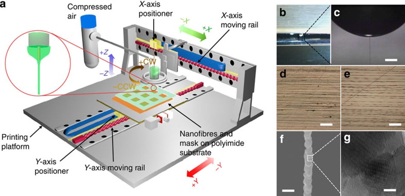
The schematic of the GNW printing system is illustrated in Fig. 1a with the printing process detailed in the Methods section. The printing system was retrofitted from a materials ink-jet printer (Dimatix, DMP 2831). Specifically, a 10 ml syringe with 50 μm diameter needle for near-field electrospinning was mounted on the printing head which moves along x-axis controlled by a step motor, and a plastic substrate was placed on the conductive platform, which is motorized along the y-axis. It is noteworthy that electrospinning is a widely used technique to fabricate organic and inorganic nanofibres and NWs with high throughput14,15,16,17,18. However, the electrospun NWs have rarely been explored for optoelectronic devices. In this work, zinc acetate (ZnAc) was mixed in PVA (polyvinyl alcohol) as the solution for electrospinning. The distance between the needle and the substrate was set to be ~300 μm. It was found that continuous electrospinning of ZnAc/PVA composite nanofibres occurred with 2 kV direct-current bias between the needle and the substrate, as shown in Fig. 1b,c and the Supplementary Video. Proper velocity control of the syringe moving along x-axis resulted in the deposition of a straight nanofibres on the substrate. Coupled with a programmable step motion along y-axis, parallel arrays of nanofibres were formed in this fashion. Notably, as the y-step size can be controlled, the spacing between the neighbouring nanofibres can be tuned. Figure 1d,e shows the two parallel array of nanofibre with the spacing set as 5 μm and 10 μm, respectively. Although the interval between nanofibres is not perfectly uniform due to a lack of feedback control on the electrospinning process, the density of nanofibres can be already controlled at an acceptable level. This can be further exemplified with the Supplementary Fig. 1a,b in which spacings of 20 μm and 30 μm between nanofibres were designed. With this approach, nanofibre arrays with tens of centimetre scale can be fabricated on either rigid or flexible substrates. More importantly, it was discovered that the nanofibre arrays can be conveniently patterned on the receiving substrate simply with a shadow mask, as shown in the schematic of Fig. 1a. This unique capability opens up the possibility for future heterogeneous integration of various types of materials for functional devices and circuits19.
Figure 1. Schematic of two-step all-printable process and materials characterization.
(a) Printing setup schematic. (b,c) Electrospinning ejection from the taylor cone apex. Scale bar, 200 μm. (d,e) Optical images of the as-printed electrospun ZnAc/PVA nanofibres with 5 μm and 10 μm spacing, respectively. Scale bars, 100 μm. (f) SEM image of an as-calcinated ZnO GNW. Scale bar, 200 nm. (g) Transmission electron microscopy image of a GNW. Scale bar, 10 nm.
Notably, it can be seen that even though most of the nanofibres in Fig. 1d are straight, there are some local spirals. This can be explained by relatively slow motion of the printing head while printing nanofibres with small line spacings (Supplementary Fig. 2)14. After printing of ZnAc/PVA composite nanofibres, ZnO GNWs were obtained via thermal calcination (Methods section) at 420 °C which is the highest temperature that polyimide substrates can withstand, while PVA has reasonable mass loss rate20. Figure 1f shows the scanning electron microscopy image of an obtained ZnO GNW with diameter~100 nm and clear polycrystalline morphology, which is further confirmed by transmission electron microscopy images shown in Fig. 1g and Supplementary Fig. 3. Furthermore, X-ray diffraction data shown in Supplementary Fig. 1c indicates formation of polycrystalline phase after calcination. In order to investigate optoelectronic properties of the arrayed ZnO GNWs, source and drain electrodes were ink-jet printed onto the GNWs with a spacing of ~2 μm between the electrodes (Methods section).
GNW photodetector performance characterization
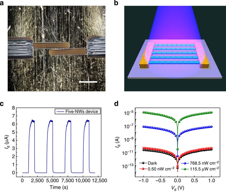
Figure 2a shows an example of the fabricated device. As the length of the electrodes and the density of the GNWs are all controllable, number of GNWs channels is tunable. Figure 2b shows a schematic of a photodetector device with five GNWs. The time-domain photoresponse of the five-GNW photodetectors was measured by periodically switching a 365 nm wavelength ultraviolet (UV) light source with intensity of 77.5 μW cm−2, as shown in Fig. 2c. It was found that the photocurrent can be readily switched between ‘OFF’ and ‘ON’ states with currents of 20 pA and 6.5 μA at 1 V bias, respectively. Furthermore, Fig. 2d shows I–V characteristics of the device measured under dark and 0.5 nW cm−2, 768.5 nW cm−2 and 115.5 μW cm−2. These results suggest that ON/OFF ratios of five orders of magnitude can be obtained for light intensities of ~100 μW cm−2 at 1 V bias, which has been rarely reported previously to our best knowledge. This high ON/OFF ratio is the result of both a high light current and a low dark current, which also renders device considerable response to extremely low light intensity down to 0.5 nW cm−2. Notably, the level of the measured current can be increased by fabricating photodetectors with more parallel GNWs. In Supplementary Fig. 4a,b, the time domain response and I–V characteristics of a device with 50 GNWs are shown. In addition, the device output current was found to be~10 times higher as compared with the device with only five GNWs.
Figure 2. Photoresponse measurement of the printed ZnO GNWs photodetectors.
(a) Optical image of an all printed GNW photodetector. Scale bar, 50 μm. (b) Schematic of a printed ZnO GNWs photodetector under UV illumination. (c) Time domain photoresponse of a GNW photodetector with five NWs under UV irradiance of 77.5 μW cm−2 at +1 V bias voltage. (d) I–V curves of the printed GNW photodetector under dark, 0.5 nW cm−2, 768.5 nW cm−2, and 115.5 μW cm−2 of UV illumination at +1 V bias voltage.
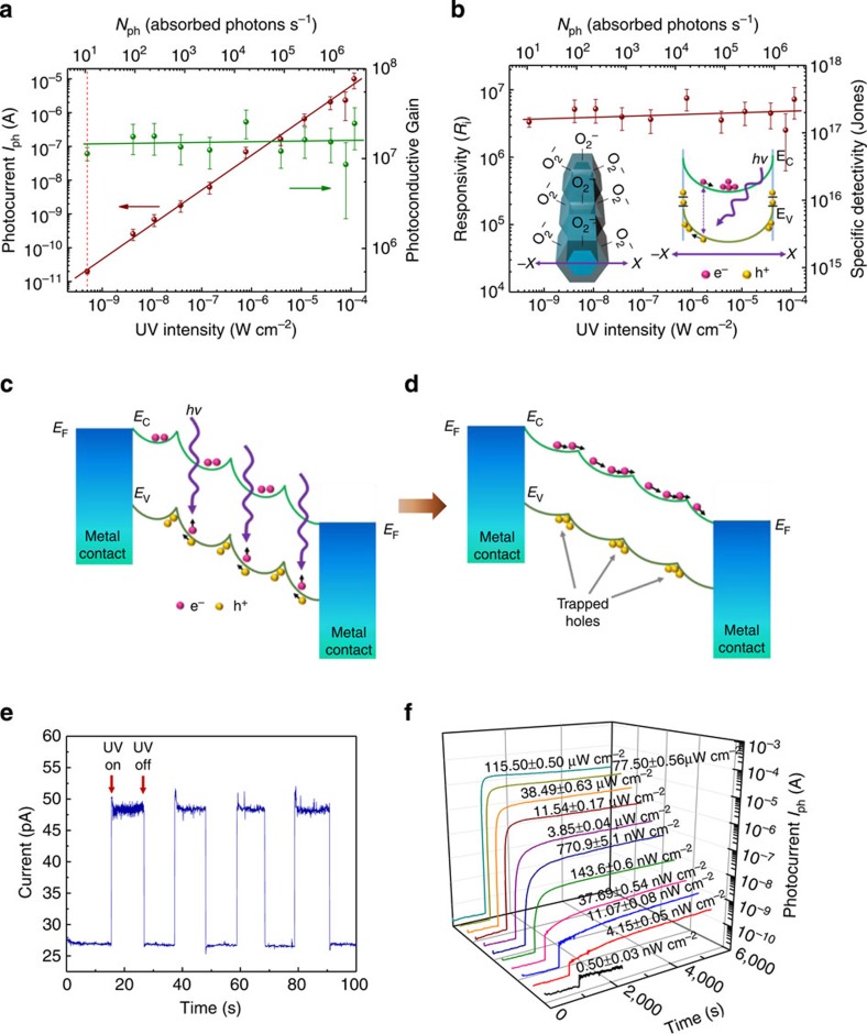
Figure 2d demonstrates that the GNW photodetector has a wide intensity response range. In our experiments, an UV lamp with wavelength of 365 nm and output power of 1 mW cm−2 was used as the light source, and different lower intensities down to 0.5 nW cm−2 were achieved with various combinations of neutral density filters. Figure 3a (wine colour plot) shows the photocurrent, Iph=Ilight−Idark, measured at different UV intensities. In order to achieve statistical results, six measurements were performed for each UV intensity with 30 mins time interval and the first measurement for each intensity was performed 15 mins after the UV intensity was established. Overall, the photocurrents in Fig. 3a show reasonable stability and statistical errors, as well as a good linearity across six orders of magnitude intensity range due to relatively low excitation intensity. Note that high photon flux can lead to saturation and sublinearity of photocurrent versus excitation intensity13,19. In fact, LDR is one of the important figure-of-merits for a photodetector and it can be calculated as21:
Figure 3. Performance characterization of GNWs photodetectors.
(a) Photocurrent and photoconductive gain of a GNW photodetector as a function of UV excitation intensity from 0.5 nW cm−2 to 115.5 μW cm−2 measured with +1 V bias. The error bars represent s.d. of multiple measurements of photocurrent for each light intensity. (b) The corresponding responsivity and specific detectivity of the GNW photodetector. Inset: schematic of oxygen adsorption on NW surface and the resulting radial direction band bending. The error bars represent s.d. of multiple measurements of photocurrent for each light intensity. (c,d) Schematics of carrier transport mechanism in the GNW photodetector upon UV illumination. (e) Time domain photoresponse of the GNW photodetector under low UV intensity of 0.5 nW cm−2 at +1 V bias voltage by manually turning on and off the UV light source. (f) The photocurrents time domain measurements of ZnO GNWs photodetector at UV intensity ranging from 0.5 nW cm−2 to 115.5 μW cm−2 with +1 V bias.
 |
where J*ph is the photocurrent and Jdark is the dark current. Following this expression, the LDR of a typical ZnO GNW photodetector was calculated as 114 dB, and this large LDR has not yet been reported for any NW-based photodector. Moreover, it is still an underestimation since the photocurrent for the highest UV intensity tested is still on the linear trend, and the lower boundary of the used UV intensity, that is, 0.5 nW cm−2, was limited by the detection limit of our UV power metre. Furthermore, the statistical number of the absorbed photons Nph for the five-GNW device was also calculated following:
 |
where P0 is the incident power density (W cm−2), d=120 nm and L=2 μm are diameter and length of a GNW between electrodes. Nph for corresponding UV intensity has been plotted as the upper x-axis in Fig. 3a. Intriguingly, it can be seen that the lowest measured UV intensity, that is, 0.5 nW cm−2, corresponds to Nph as low as 12 photons per second for the GNW device. It is worth mentioning that this is an estimation based on the assumption that the cross-sectional area of NWs is the active area to absorb the normal incident light13,22; in reality, there could be scattered light coupled into the NWs from metal electrodes23, underneath substrate24 and so on. Nevertheless, this qualitatively shows the high sensitivity of a GNW photodetector.
On the basis of the dependence of photocurrent over UV light intensity and photon flux, a more quantitative characteristics and analysis of the GNW photodetector has been achieved, including photoconductive gain (G), responsivity (Ri) and specific detectivity (D*). By definition, G reflects the ratio of the number of charge carrier circulating in the circuit over the number of photons absorbed in the device with five GNWs, that is,
 |
The olive colour plot in Fig. 3a demonstrates that a consistently high photoconductive gain across a broad light intensity range can be achieved with the maximum Gmax=2.6 × 10⁷. Meanwhile, in order to examine the response of the photocurrent to incident optical power, the responsivity of the device is calculated following the expression22:
 |
where Popt is the illumination power on the active area13,22 of a GNW device Popt=P0 × d × L × 5. The left axis of Fig. 3b shows the scale of Ri. It can be conspicuously seen that a high responsivity of up to Rimax=7.5 × 10⁶ (AW−1) can be obtained from the GNW device. High gain and responsivity indicate large electrical output signals, for example, photocurrent, can be achieved with relatively low optical input. Besides gain and responsivity, the specific detectivity is also one of the key figure-of-merits for a photodetector, which usually describes the smallest detectable signal21,25,26:
 |
 |
where A is the effective area of the detector in cm2, B is bandwidth, NEP is the noise equivalent power, 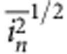 is the measured noise current and Ri is the responsivity. If the shot noise from the dark current is the major contribution to the noise limiting the detectivity, then the detectivity can be simplified as21:
 |
In this case, A is the total cross-sectional area of the five GNWs; thus, Idark/A gives dark current density. Equation (7) suggests that the high responsivity and the low dark current will naturally lead to high detectivities. The right side vertical axis of Fig. 3b shows at 1 V bias a detectivity D* as high as 3.3 × 10¹⁷ Jones has been achieved. It is worth pointing out that such a high detectivity provides quantitative evidence that a GNW photodetector is extremely sensitive to small optical input signals. In addition, a detectivity as high as 1017 Jones has not been reported for single-crystalline NWs device previously, primarily due to the difficulty to achieve high responsivity and low dark current at the same time.
The above systematic studies have shown the high performance of the GNW photodectors. Overall, GNW photodetectors have demonstrated photoconductive gains of 2.6 × 10⁷ at 1 V bias, which are comparable to the reported record for single-crystalline NW photodetectors (2 × 10⁸ at 5 V bias13). In addition, they have shown the highest responsivity and detectivity among the reports for nanomaterial-based photodetectors. For single-crystalline NW photodetectors, it is commonly accepted that the high photoconductive gain originates from the presence of oxygen-related hole-trap states at the NW surface. These states tend to adsorb oxygen molecules from air causing capture of free electrons in the NW, namely,  (refs 11, 13, 27). Electron depletion at the NW surface induces surface band bending, as shown in the inset of Fig. 3b6,13,28. Such a surface band bending establishes an internal electric field in radial direction, which can spatially separate photo-generated electron-holes leading to suppressed photocarrier recombination and dramatically prolonged carrier life-times13,29. Meanwhile, it has also been reported that photo-generated holes can participate in oxygen desorption on the surface, which can in turn release back the captured free electrons, leading to further increase of free carrier concentration13,30. These coupled mechanisms result in high photoconductive gains of single-crystalline NW photodetectors made of ZnO13 and other materials, including InAs31, CdS32, In2O333, SnO234,35. Nevertheless, in this case, energy band-edge bending/modulation is observed only in NW radial direction, while the core of the NW is the fast track for electron transport for a typical n-type material. Therefore, when there are excess carriers in the NW at room temperature due to thermal activation without light illumination, the dark current of the photodetector is inevitably high, which will limit the dynamic response range and detectivity of the photodector. In comparison with single-crystalline NWs, GNWs also have a large surface area with rich surface states, which can lead to high photoconductive gain following the same mechanisms discussed above. As a matter of fact, a GNW can have even larger surface area as compared with a single-crystalline NW with the same diameter, due to the surface roughness and granular morphology. Meanwhile, a GNW is still inherently different from a single-crystalline NW due to the existence of crystalline grains and grain boundaries, as evidenced by the images shown in Fig. 1f,g. These grain boundaries serve as energy barriers for carrier transport in dark condition and introduce additional band-edge modulation along axial direction of the GNW, as schematically shown in Fig. 3c36,37. As a result, the dark current of the GNW photodetector can be greatly suppressed. On UV illumination, excessive photo-generated holes can migrate to grain boundaries, driven by the established internal electric field, as shown in Fig. 3c,d, , , leading to the lowered barrier height. As the electrons transport across these barriers via tunnelling and thermionic emission, the emission current is extremely sensitive to barrier height modulation38, as illustrated in Fig. 3d, . Eventually, a GNW photodetector can demonstrate a high current gain in this fashion. In fact, this gain mechanism is akin to that for the ‘blocking contact’ thin film photodetector reported earlier by Mehta and Sharma39, even though it was the Schottky barrier width, rather than the height, that was being modulated. Furthermore, in the case of GNWs there are obviously multiple barriers along the NW axial direction. Notably, it has been shown in Fig. 3a that the GNW photodetector is responsive to extremely low light intensities down to 0.5 nW cm−2. This fact indicates that it is not necessary to lower all the axial energy barriers at the grain boundaries in order to obtain a detectable photon current. As these axial Schottky barriers have rather low barrier heights36, single photon absorption events occurring in one grain reduce the local barrier height and driven by the external field can lead to the transport and acceleration of multiple carriers to the neighbouring grain. Thus, these carriers can carry a higher energy to assist more carriers being emitted through the unlowered barriers, as schematically shown in the Supplementary Fig. 5. Such a gain process is a carrier multiplication process triggered by lowering of axial Schottky barrier height. Moreover, this process is expected to be much faster than the oxygen adsorption/desorption process. Under high photon flux illumination, large population of holes move toward the NW surface and trigger oxygen desorption process, which in turn releases the captured electrons back to the conduction channel, as discussed in the aforementioned text. However, this is a rather slow process, resulting in photocurrent rise times as long as minutes, as evident in Fig. 2c13,35. Nevertheless, Fig. 3e shows the time domain response of the GNW device to UV intensities of 0.5 nW cm−2. It can be seen that response of the device to such a low intensity is relatively fast and consistent. Specifically, the rise time (τr, defined as rising time from 10% to 90% of maximum photocurrent40) and decay time (τd, defined as falling time from 90% to 10% of maximum photocurrent40) were measured as 0.56 s and 0.32 s, respectively, as shown in Supplementary Fig. 6. Meanwhile, photocurrent rise times for all UV intensities ranging from 0.5 nW cm−2 to 115.5 μW cm−2 were measured, and are shown in Fig. 3f. It confirms that when the UV intensity is below 100 nW cm−2, the rise of the photocurrent is much faster than that for higher intensities.
Device modelling
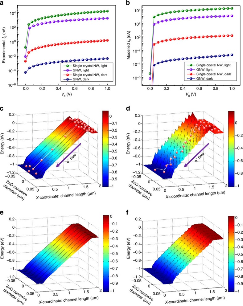
To further confirm the above discussed gain mechanism, device simulation was carried out using SILVACO (version #2012). The details of the simulation setup can be found in Method section. In this case, both single-crystalline ZnO NWs and GNWs were modelled. In addition, in order to build Schottky barriers at the grain boundaries, a 10 nm p-type ZnO region was inserted between n-type grains. This approach was adopted from previous investigation on thin film devices36,41. Figure 4a,b shows the experimental and the simulated I–V curves of individual single-crystalline and GNW devices modelled in both dark and light condition. The light intensity for experiments and simulations are both 100 μW cm−2, at 365 nm wavelength. It can be seen that the trends for simulation and experiments are highly consistent. Namely, the single-crystalline NWs have both higher dark and higher light currents than the GNWs. Importantly, even though the light current of the GNWs is lower than that of the single-crystalline NWs within one order of magnitude, the suppression of the dark current is around three orders of magnitude. The effective reduction of the dark current can logically explain the large LDR and high detectivity discussed above. Furthermore, conduction band-edge energy profiles of the single-crystalline NW and GNW under dark and light conditions have been plotted and are shown in Fig. 4c–f. The band-edge modulation along axial direction for the GNW is clearly visualized in Fig. 4d. Such band modulation naturally leads to more difficult electron transport as illustrated in Fig. 4d. On UV illumination, the energy profile of the single-crystalline NW (Fig. 4e) does not change; however, the energy profile for the GNW appears to be much more flat (Fig. 4f), which is consistent with the picture presented in Fig. 3c,d. Note that even though the barrier height is largely reduced, the existence of barriers still leads to lower light currents as compared to single-crystalline NWs, as evident in Fig. 4a,b.
Figure 4. Device modeling of a GNW photodetector.
Comparison of the experimental (a) and modelled (b) I–V curves of photodetectors made of an individual single crystal ZnO NW and a GNW. (c) and (d) are modelled conduction band energy profiles of a single crystalline NW device and a GNW device under dark condition, respectively. And (e) and (f) are the corresponding modelled results under 100 μW cm−2 UV illumination, respectively.
Photoconductivity spectra analysis
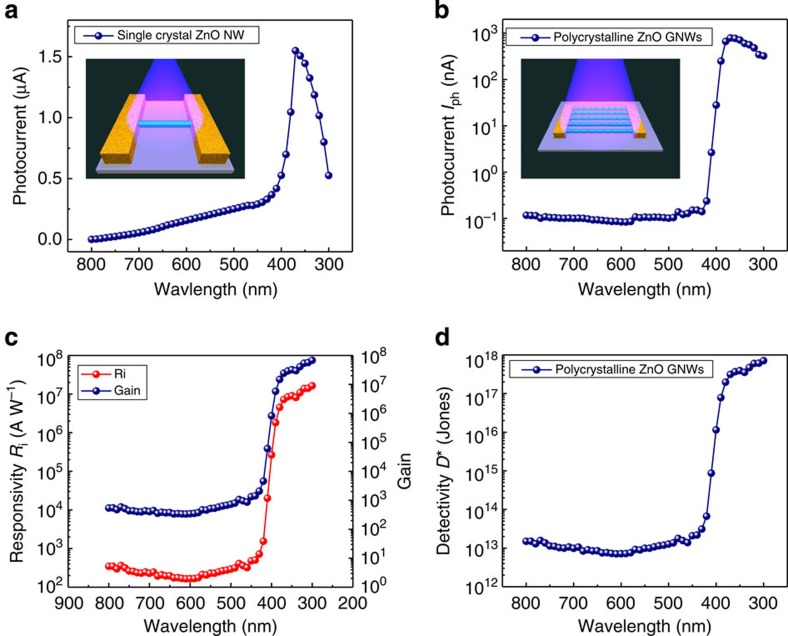
The above investigations are more focussed on the response characteristics of GNW devices to 365 nm UV light. In fact, the spectral response of a photodetector is also of great importance and is shown in Fig. 5. Figure 5a,b demonstrates photocurrent spectra for an individual single-crystalline ZnO NW (Supplementary Fig. 7) and five GNW for comparison. Note that the intensity of light at 370 nm wavelength was measured as 9.1 μW cm−2 (Supplementary Fig. 8). It can be seen that although the single-crystalline NW has a high photocurrent for UV light, it responds to longer wavelength as well. However, the GNW device demonstrates four orders of magnitude selectivity for 365 nm over 600 nm wavelength. This visible-blind UV sensing is certainly highly attractive for practical applications. This observation is not unexpected as single-crystalline ZnO NWs grown with chemical vapour deposition method using Zn powder and low-concentration oxygen as precursor have been shown to possess defect energy levels in the band-gap due to the existence of Zn interstitials and oxygen vacancies5,30,42. These defect states render a rather broad absorption spectrum for the chemical vapour deposition grown NWs. Meanwhile, the GNWs were obtained by calcination in air which has close to 20% oxygen. Therefore, the concentration of the aforementioned defects can be minimized. On the basis of the photocurrent spectrum of the GNW device, its responsivity, gain and detectivity spectra have been obtained and are shown in Fig. 5c,d, respectively. These data not only show the high performance consistent with Fig. 3a,b for 365 nm wavelength, but also indicate that even higher responsivity, gain and detectivity can be achieved for shorter wavelength such as 300 nm.
Figure 5. Spectral characterization of the photodetectors.
Photoconduction spectra of a single crystal NW device (a) and a GNW device (b), with wavelength ranging from 300 nm to 800 nm. (c) The corresponding responsivity and photoconductive gain versus incident wavelength of the GNW device. (d) The corresponding detectivity versus incident wavelength of the GNW device.
Flexible device fabrication and characterization
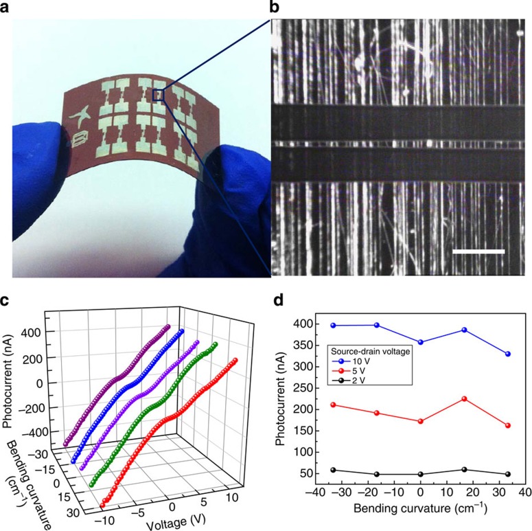
The above systematic investigations have shown the great potential of GNWs for high-performance UV detection. The discovered mechanisms can be used as guidelines to design high-performance photodetectors with other material systems thus different colour detection is feasible. Meanwhile, a reliable and low-cost fabrication process is equally important from a practical point of view. Inherently, the reported all-printable GNW fabrication process is cost-effective and scalable and is compatible with various types of substrates. Particularly, GNWs and metal electrodes have been printed onto polyimide substrates, as shown in Fig. 6a,b. The sample is largely flexible, as can be seen from Fig. 6a and was measured under different bending curvatures using the indoor incandescent light. As shown in Fig. 6c, the I–V curves are almost identical for different bending curvatures. Meanwhile, Fig. 6d shows the relative change of current at different bias with respect to the non-bending I–V curve, confirming the robustness of the device. This result indicates that GNWs and the fabrication process can be potentially used for low-cost flexible and portable devices in the future.
Figure 6. Flexible all-printable device and bending measurements.
(a) Optical image of a flexible all-printable GNW photodetector array. (b) Optical images of the printed GNWs and Ag electrodes. Scale bar, 30 μm. (c) I–V curves of the flexible GNW device obtained at different bent curvatures under indoor incandescent light condition. (d) Photocurrent stability test for different bending curvatures.
Discussion
In summary, we have demonstrated all-printable fabrication of polycrystalline ZnO GNW photodetectors. Such a fabrication process is scalable, cost-effective and compatible to rigid and flexible substrates. Systematic investigations on the photodetection properties of the devices have been carried out, revealing their excellent performance including high photoconductive gain, responsivity and detectivity. Particularly, the obtained responsivity and detectivity are among the highest from the existing reports for NW-based devices. Our analysis shows that their high performance originates from the unique band-edge modulation along the GNW axial direction. The existence of Schottky barriers in series leads to highly suppressed dark current of the device, and it also gives rise to a fast photoelectric response to low intensity optical signal due to the barrier height modulation. The discovered rationale in this work can be utilized as a guideline to design high-performance photodetectors with other nanomaterial systems as well. Meanwhile, the developed fabrication process opens up possibility for future flexible and high performance electronic and optoelectronic circuitry.
Methods
ZnO GNW Electrospun solution preparation
2 g PVA and 18 g deionized water mixture was stirred at 105 °C with 380 r.p.m. until fully dissolved. Then 1.5 g ZnAc and 2 g deionized water was also stirred at 60 °C water bath with 420 r.p.m. for 2 h. Thereafter, the cooled PVA mixture solution was slowly poured into the ZnAc solution while kept on stirring for 2 h until complete intermixing. Then the precursor solution was kept overnight before the subsequent electrospinning.
Near-field electrospinning and printing of ZnO GNWs
The prepared electrospinning precursor solution was injected into a syringe with 50 μm inner diameter which is mounted onto the DMP 2831 materials printer header, as shown in Fig. 1a. Then a 20 μm diameter copper wire was inserted into the syringe and the syringe needle to control the solution droplet falling speed and serve as anode in the meantime. The distance between the syringe needle and the electrically grounded metal motorized stage was set as 400 μm–1.5 mm. Then a printing substrate, such as polyimide, glass, or Si, was placed on the stage and under the syringe needle to achieve ~300 μm distance from the substrate surface to the needle. In order to pattern the GNW array, a shadow mask made of thin metal foil was placed on top of the printing substrate, as shown in Fig. 1a and the Supplementary Video. To start the printing process, +2 kV was applied to the copper wire anode to establish stable electrospinning as shown in Fig. 1c. Then the programme started x scan of the printing head at adjustable velocity by tuning dot to dot drop spacing. By setting the y interval of the neighbouring scan lines, the GNW printing density could be readily controlled as 5, 10, 20 and 30 μm respectively. After printing, the sample was calcinated in a tube furnace at 420 °C for 2 h before printing of silver electrodes.
Ink-jet printing of silver electrodes
After calcination, the silver nanoparticle ink was printed onto the GNW arrays following the predesigned source and drain patterns. Then the chip was baked at 150 °C for 30 min to remove the organic components in the silver ink and improve the conductivity of the silver electrodes.
GNWs photodetector performance characterization
GNW photodetector I–V measurements in the dark and under different UV intensity illumination were performed by applying an external bias (V=1 V) to the GNWs device in the probe station and recorded by semiconductor parameter analyser (HP4156A). A 1 mW cm−2 365 nm wavelength UV lamp was used as the UV source. The optical power intensity illuminated on the GNW photodetectors was tuned by using various combinations of neutral density filters and calibrated with a UV enhanced silicon photodetector (Newport, 918D-UV-OD3R). The photocurrent spectra were measured by using the output light from a quantum efficiency measurement system (Newoport, QE-PV-SI QE/IPCE Measurement Kit) as the tunable wavelength light source. The photocurrent was recorded with a Keithley 2400 source meter.
Silvaco device simulation
The device simulations on single-crystalline NWs and GNWs shown in Fig. 4 were obtained by using Silvaco Atlas 3-D cylindrical model. The length and diameter of the NWs were set as 2 μm and 100 nm, respectively. For the GNWs, the grain size was set as 100 nm according to the SEM image and the boundary width was set as 10 nm. Since the length of source and drain electrode contacts was set as 100 nm, the part of a NW in between source and drain electrodes was 1.8 μm long, which was surrounded by ambient air. Therefore, there were a total of 16 grain boundaries created along the axis of a GNW. The Schottky barrier at the grain boundaries was produced by specifying different doping type in grain regions and boundary regions, as similar methods have been done to analyse the behaviours of ZnO thin films34,36,39,41. Specifically, the doping of a single-crystalline NW and the grain regions of a GNW were set as n-type with an electron concentration of 1.6 × 1017 cm−3. The grain boundary regions were set as p-type with hole concentration of 1.6 × 1012 cm−3. In addition, the n-type doping was uniformly distributed and the p-type doping was of Gaussian distribution with 10 nm characteristic length. The concentration of acceptor type surface trap was set as 3 × 1011 cm−3 at NW–air interface. In the simulations, 365 nm wavelength UV light with 1 × 10⁻⁴ W cm−2 intensity was shone onto the NWs normal to the axis of nanowire, and +1 V voltage was applied to the drain terminal and the resulting I–V characteristics are plotted in Fig. 4a,b. The conduction band energy profiles were also obtained and plotted in Fig. 4c–f.
Author contributions
X.L., L.G., Q.Z., Y.L. and Z.F. designed the experiments. X.L., L.G., Q.Z., Y.L. and Z.F. carried out the experiments. X.L. and J.W. performed Silvaco simulations. X.L., L.G., Q.Z., J.W., Y.L. and Z.F. contributed to data analysis. X.L. and Z.F. wrote the paper and all authors provided feedback.
Additional information
How to cite this article: Liu, X. et al. All-printable band-edge modulated ZnO nanowire photodetectors with ultra-high detectivity. Nat. Commun. 5:4007 doi: 10.1038/ncomms5007 (2014).
Supplementary Material
Supplementary Figures 1-8
Supplementary Video of printing nanofibers. ZnAc/PVA composite fiber printing-2KV DC bias was applied between the metal syringe needle and the metal platform covered by a piece of paper, a polyimide substrate and a metal printing mask. The syringe needle was mounted on the printing head and the X-Y translation was driven by step motors controlled by a computer.
Acknowledgments
We thank Shengwang Du from the Department of Physics, HKUST for discussion and Materials Characterization and Preparation Facility (MCPF) for technical assistance. This work was supported by research grants from the HK Innovation and Technology Fund ITS/192/11 and Early Career Scheme 623112, General Research Fund 612111 and 612113 from Research Grant Council, Hong Kong.
References
- Hua B., Wang B., Yu M., Leu P. W. & Fan Z. Rational geometrical design of multi-diameter nanopillars for efficient light harvesting. Nano Energy 2, 951–957 (2013). [Google Scholar]
- Cao L. Y. et al. Engineering light absorption in semiconductor nanowire devices. Nat. Mater. 8, 643–647 (2009). [DOI] [PubMed] [Google Scholar]
- Kim P., Shi L., Majumdar A. & McEuen P. Thermal transport measurements of individual multiwalled nanotubes. Phys. Rev. Lett. 87, 215502 (2001). [DOI] [PubMed] [Google Scholar]
- Nam D. et al. Strain-induced pseudo-heterostructure nanowires confining carriers at room temperature with nanoscale-tunable band profiles. Nano Lett. 13, 3118–3123 (2013). [DOI] [PubMed] [Google Scholar]
- Fan Z. Y. & Lu J. G. Chemical sensing with ZnO nanowire field-effect transistor. IEEE Trans. Nano 5, 393–396 (2006). [Google Scholar]
- Pan X., Liu X., Bermak A. & Fan Z. Self-gating effect induced large performance improvement of ZnO nanocomb gas sensors. ACS Nano 7, 9318–9324 (2013). [DOI] [PubMed] [Google Scholar]
- Liu X., Long Y., Liao L., Duan X. & Fan Z. Large-scale integration of semiconductor nanowires for high-performance flexible electronics. ACS Nano 6, 1888–1900 (2012). [DOI] [PubMed] [Google Scholar]
- Fan Z. Y. et al. Three-dimensional nanopillar-array photovoltaics on low-cost and flexible substrate. Nat. Mater. 8, 648–653 (2009). [DOI] [PubMed] [Google Scholar]
- Fan Z. Y. et al. Toward the development of printable nanowire electronics and sensors. Adv. Mater. 21, 3730–3743 (2009). [Google Scholar]
- Fan Z. Y. & Lu J. G. Gate-refreshable nanowire chemical sensors. Appl. Phys. Lett. 86, 123510 (2005). [Google Scholar]
- Fan Z. Y., Wang D. W., Chang P. C., Tseng W. Y. & Lu J. G. ZnO nanowire field-effect transistor and oxygen sensing property. Appl. Phys. Lett. 85, 5923–5925 (2004). [Google Scholar]
- Skucha K., Fan Z., Jeon K., Javey A. & Boser B. Palladium/silicon nanowire schottky barrier based hydrogen sensors. Sensor. Actuat. B-Chem. 145, 232–238 (2010). [Google Scholar]
- Soci C. et al. ZnO nanowire UV photodetectors with high internal gain. Nano Lett. 7, 1003–1009 (2007). [DOI] [PubMed] [Google Scholar]
- Sun D., Chang C., Li S. & Lin L. Near-field electrospinning. Nano Lett. 6, 839–842 (2006). [DOI] [PubMed] [Google Scholar]
- Zheng G. et al. Precision deposition of a nanofibre by near-field electrospinning. J. Phys. D 43, 415501 (2010). [Google Scholar]
- Bisht G. S. et al. Controlled continuous patterning of polymeric nanofibers on three-dimensional substrates using low-voltage near-field electrospinning. Nano Lett. 11, 1831–1837 (2011). [DOI] [PubMed] [Google Scholar]
- Chang C., Limkrailassiri K. & Lin L. Continuous near-field electrospinning for large area deposition of orderly nanofiber patterns. Appl. Phys. Lett. 93, 123111–123113 (2008). [Google Scholar]
- Cho H., Min S. & Lee T. Electrospun organic nanofiber electronics and photonics. Macromol. Mater. Eng. 298, 475–486 (2013). [Google Scholar]
- Fan Z. Y., Ho J. C., Jacobson Z. A., Razavi H. & Javey A. Large-scale, heterogeneous integration of nanowire arrays for image sensor circuitry. Proc. Natl Acad. Sci. USA 105, 11066–11070 (2008). [DOI] [PMC free article] [PubMed] [Google Scholar]
- Gilman J. W., VanderHart D. L. & Kashiwagi T. Thermal decomposition chemistry of poly (vinyl alcohol). ACS Sym. Ser. 599, 161–185 (1994). [Google Scholar]
- Gong X. et al. High-detectivity polymer photodetectors with spectral response from 300 nm to 1450, nm. Science 325, 1665–1667 (2009). [DOI] [PubMed] [Google Scholar]
- Yang Q. et al. Enhancing sensitivity of a single ZnO micro-/nanowire photodetector by piezo-phototronic effect. ACS Nano 4, 6285–6291 (2010). [DOI] [PubMed] [Google Scholar]
- Fan P., Huang K. C., Cao L. & Brongersma M. L. Redesigning photodetector electrodes as an optical antenna. Nano Lett. 13, 392–396 (2013). [DOI] [PubMed] [Google Scholar]
- Li Z. et al. Effect of a proximal substrate on plasmon propagation in silver nanowires. Phys. Rev. B 82, 241402 (2010). [Google Scholar]
- Liu J. inPhotonic Devices Cambridge University Press Cambridge (2005). [Google Scholar]
- Guo F. et al. A nanocomposite ultraviolet photodetector based on interfacial trap-controlled charge injection. Nat. Nanotech. 7, 798–802 (2012). [DOI] [PubMed] [Google Scholar]
- Kong J. et al. Nanotube molecular wires as chemical sensors. Science 287, 622–625 (2000). [DOI] [PubMed] [Google Scholar]
- Chen C. et al. Probing surface band bending of surface-engineered metal oxide nanowires. ACS Nano 6, 9366–9372 (2012). [DOI] [PubMed] [Google Scholar]
- Chen M., Retamal J. R. D., Chen C. & He J. Photocarrier relaxation behavior of a single ZnO nanowire UV photodetector: effect of surface band bending. IEEE Electron Device Lett. 33, 411–413 (2012). [Google Scholar]
- Fan Z. Y. et al. Photoluminescence and polarized photodetection of single ZnO nanowires. Appl. Phys. Lett. 85, 6128–6130 (2004). [Google Scholar]
- Liu Z. et al. High-detectivity InAs nanowire photodetectors with spectral response from ultraviolet to near-infrared. Nano Res. 6, 775–783 (2013). [Google Scholar]
- Jie J. S. et al. Photoconductive characteristics of single-crystal CdS nanoribbons. Nano Lett. 6, 1887–1892 (2006). [DOI] [PubMed] [Google Scholar]
- Zhang D. et al. Ultraviolet photodetection properties of indium oxide nanowires. Appl. Phys. A Mater. Sci. Progress 77, 163–166 (2003). [Google Scholar]
- Mathur S., Barth S., Shen H., Pyun J. & Werner U. Size-dependent photoconductance in SnO2 nanowires. Small 1, 713–717 (2005). [DOI] [PubMed] [Google Scholar]
- Hu L., Yan J., Liao M., Wu L. & Fang X. Ultrahigh external quantum efficiency from thin SnO2 nanowire ultraviolet photodetectors. Small 7, 1012–1017 (2011). [DOI] [PubMed] [Google Scholar]
- Hossain F. M. et al. Modeling and simulation of polycrystalline ZnO thin-film transistors. J. Appl. Phys. 94, 7768–7777 (2003). [Google Scholar]
- Hossain F. M. et al. Modeling of grain boundary barrier modulation in ZnO invisible thin film transistors. Physica E 21, 911–915 (2004). [Google Scholar]
- Sze S. M. & Ng K. K. inPhysics of Semiconductor Devices Wiley-interscience (2006). [Google Scholar]
- Mehta R. & Sharma B. Photoconductive gain greater than unity in CdSe films with Schottky barriers at the contacts. J. Appl. Phys. 44, 325–328 (1973). [Google Scholar]
- Decoster D. & Harari J. inOptoelectronic Sensors Wiley-ISTE (2010). [Google Scholar]
- Yamaguchi K. Modeling and characterization of polycrystalline-silicon thin-film transistors with a channel-length comparable to a grain size. J. Appl. Phys. 89, 590–595 (2001). [Google Scholar]
- Chang P. C. et al. ZnO nanowires synthesized by vapor trapping CVD method. Chem. Mater. 16, 5133–5137 (2004). [Google Scholar]
Associated Data
This section collects any data citations, data availability statements, or supplementary materials included in this article.
Supplementary Materials
Supplementary Figures 1-8
Supplementary Video of printing nanofibers. ZnAc/PVA composite fiber printing-2KV DC bias was applied between the metal syringe needle and the metal platform covered by a piece of paper, a polyimide substrate and a metal printing mask. The syringe needle was mounted on the printing head and the X-Y translation was driven by step motors controlled by a computer.


