Abstract
It is extremely difficult to control the growth orientation of the graphene layer in comparison to Si or III–V semiconductors. Here we report a direct observation of graphene growth and domain boundary formation in a scanning transmission electron microscope, with residual hydrocarbon in the microscope chamber being used as the carbon source for in-plane graphene growth at the step-edge of bilayer graphene substrate. We show that the orientation of the growth is strongly influenced by the step-edge structure and areas grown from a reconstructed 5–7 edge are rotated by 30° with respect to the mother layer. Furthermore, single heteroatoms like Si may act as catalytic active sites for the step-edge growth. The findings provide an insight into the mechanism of graphene growth and defect reconstruction that can be used to tailor carbon nanostructures with desired properties.
 Direct visualization of graphene growth is highly desired, though, extremely high growth rates during chemical vapour deposition make atomic resolution analysis infeasible. Here, Liu et al. report the visualization of the in situ in-plane growth of graphene in a scanning transmission electron microscope.
Since the first demonstration of producing graphene layers by mechanical exfoliation of bulk graphite1, many growth or synthesis approaches for producing few-layer graphene have been investigated, including chemical vapour deposition (CVD) on metal catalysts2,3,4,5,6,7,8, reduced graphene oxides9, thermal decomposition of SiC10,11 and molecular beam epitaxy12,13,14. However, in comparison with Si or III–V semiconductors, it is extremely difficult to control the growth orientation of the graphene layer, and hence its assembly in an electronic device is believed to be problematic. Direct visualization of how the graphene network evolves during growth is highly desired in an effort to precisely understand the atomic processes of the growth mechanism. Furthermore, to realize well-controlled graphene nanodevices, identifying the orientation relationship between the seed crystal and the growing layer or detecting the influence of the catalytic atoms during growth would be of immense benefit. The extremely high CVD growth rate (on the order of micrometres per minute) makes atomic resolution analysis during this method unfeasible.
The edge structures of graphene ribbons are of fundamental importance during growth and preparation processes because the electronic, optical, magnetic, mechanical and electrochemical properties depend not only on the ribbon width but also on the edge structures15,16,17,18,19,20,21,22,23,24,25. Graphene nanoribbons generally have edge structures that are a combination of armchair (AC) and zigzag (ZZ) geometries26,27, and recent theoretical calculations and experimental studies have also demonstrated the existence of an alternate pentagon–heptagon edge structure (ZZ (57)) reconstructed from a periodic hexagon ZZ structure20,28,29,30,31,32,33. Graphene nanoribbons with AC and ZZ edges have distinct electronic transport properties34, but atomic-scale edge defects can significantly affect the electronic properties35. Pristine graphene edge structures are of particular importance as they govern the quality of the subsequent synthesized material. Low-energy electron microscopy, photoemission electron microscopy and low-energy electron diffraction can give unique insight into the fundamental growth mechanisms of graphene on metal substrates36,37. Invaluable insight into the atomic structure of graphene including defects and edge stabilities has been provided by scanning tunnelling microscopy38,39 and transmission electron microscopy (TEM), especially aberration-corrected high-resolution TEM33,40,41,42,43,44,45,46,47,48, and furthermore, the electron beam can be used to modify the graphene edge structure, create single atomic C chains or nanoribbons49,50, sculpt near-defect-free graphene nanostructures48, sublimate graphene layer by layer51 and reknit holes in monolayer graphene52.
As the vacuum system in an electron microscope is not perfect, the residual hydrocarbon gas in the sample chamber can be used to grow graphene at high temperatures, although the properties of the hydrocarbon gases cannot be characterized. Here we show that graphene grows extremely slowly (several angstroms per minute) in a transmission electron microscope, allowing simultaneous growth and atomic resolution imaging. We visualize the in situ in-plane growth of graphene on the terrace of the first layer using aberration-corrected scanning TEM (STEM), and observe the activity of a single Si atom catalyst during graphene growth on an atomic scale. STEM has the added advantage in that the focused high-density electron beam is able to modify the structure of the sample, and thus, this method can be used to manipulate the graphene growth. Although Zan et al.52 have reported reknitting holes in monolayer graphene with the reknitted areas that are composed of many 5–7 defects showing an ‘amorphous’ characteristic, the mechanism of in-plane growth from a step-edge in this study is different from that of reknitting holes. Holes have a limited circumference without substrate, however, edges have a half opened space to grow graphene. More importantly, the newly grown graphene is not amorphous but crystalline in our study. The relationship between the growth speed of graphene and the residual hydrocarbon gas pressure is also investigated.
Results
Step-edge graphene growth
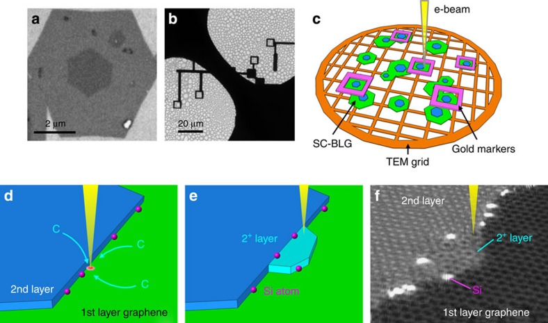
Figure 1a shows a scanning electron microscopy image of a single-crystal bilayer graphene (SC-BLG) grown using ambient pressure CVD53. Both the first and second graphene layers exhibit hexagonal shape and the macroscopically sharp edges serve as an ideal step structure for the assembly of foreign impurities. SC-BLG flakes with distinct twisting angles were marked by electron-beam (e-beam) lithography and then cleanly transferred to a Mo TEM grid as shown in Fig. 1b (ref. 53). The marked SC-BLG flakes were observed at various temperatures (T=RT to 700 °C) in an aberration-corrected STEM instrument operated at 60 kV (Fig. 1c).
Figure 1. Scheme of graphene growth by e-beam in TEM.
(a) Scanning electron microscopy image of a SC-BLG, (b) marked by e-beam lithography, (c) transferred to a Mo TEM grid and (d) schematic drawing of the 2nd-layer graphene step-edge. Hydrocarbon accumulates to the e-beam scanning area. (e) The new growth graphene layer (2+ layer, light blue) at the BLG step-edge. Single Si atoms (pink) located at the step-edge. (f) ADF image in a perspective view (the ADF image is 40° inclined respect to the vertical plane, the raw image is shown in Supplementary Fig. 3) showing the electron-beam-induced growth from the step-edge of the SC-BLG where the single Si atoms (brighter contrast) existed.
Carbon materials placed in the electron beam usually suffer from radiation damage, and Kotakoski et al.32 found that to prevent knock-on damage in graphene the electron energy should be below a threshold of ~50 kV, even for defective samples and irradiation at the edges. Knock-on damage is thus likely to be observed even at the edges of graphene under a 60-kV irradiation, but because of the imperfect vacuum (1–3 × 10⁻⁵ Pa around the specimen), graphene growth (the completely opposite phenomenon to knock-on damage) can be observed at a particular temperature when the graphene samples are heated inside the electron microscope. The nature of the residual gases inside the microscope chamber cannot be identified, but it is well known that they are a mixture of hydrocarbon gases. Hydrocarbons will agglomerate in the electron-beam scanning area and graphitize from the bilayer edge. Figure 1d,e shows the schematics of the graphene growth, and Fig. 1f shows an annular dark-field (ADF) image of the electron-beam-induced growth from the step-edge of the SC-BLG in a perspective view. At room temperature, the electron beam will usually result in contamination of the graphene surface, whereas at temperatures higher than 700 °C, growth of graphene is never found due to the high mobility of the hydrocarbon atoms.
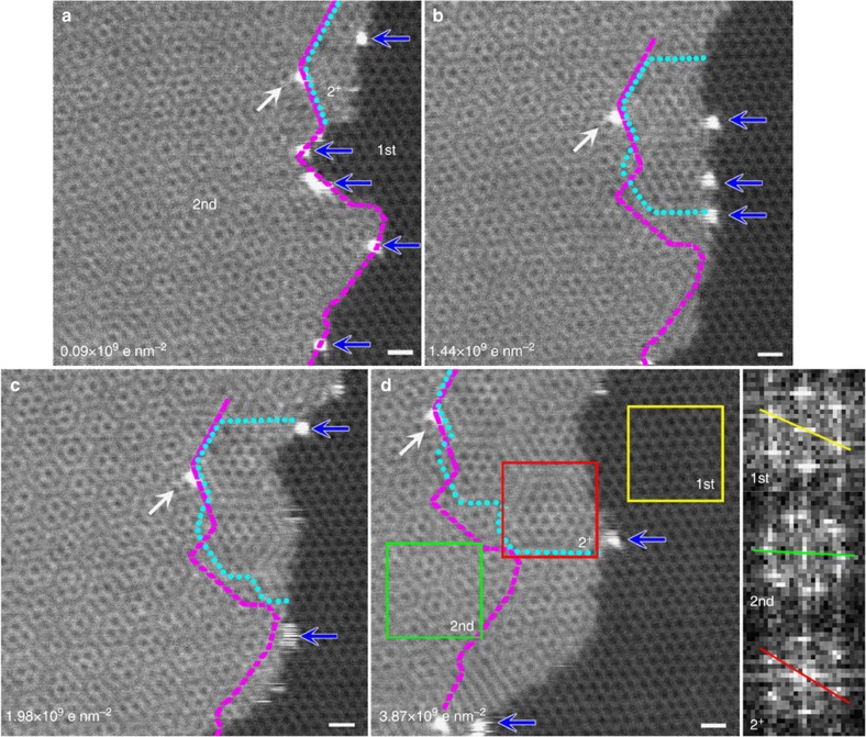
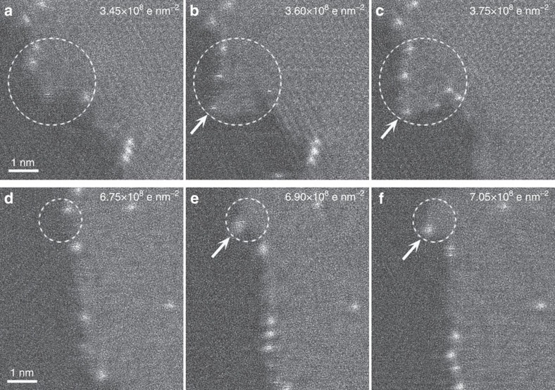
Figure 2 shows a series of ADF images of a bilayer single-domain graphene heated to 500 °C inside the microscope, revealing the growth process from the edge of the twisted bilayer graphene. To explain these results in a clear manner, we label the graphene layer with the larger planar dimension as layer 1 (or 1st) and that with the smaller area as layer 2 (or 2nd). Note, however, that this does not clarify which layer is on the top. In the corresponding Fourier transforms of the images (Fig. 2 inset), we see that the twisting angle between the two layers is about 20°. The dashed blue line in Fig. 2a indicates the new growth area at the beginning of the growing stage, and it is worth noting here that there are some isolated brighter atoms in this area. According to an analysis of the electron energy-loss spectroscopy (EELS) data (Supplementary Fig. 1), these brighter atoms are Si atoms introduced by the quartz furnace used during CVD. These Si atoms might act as catalysts during the graphene growth and slide over the graphene edges during electron-beam scanning. The possibility of catalytic effect of Si atoms can be demonstrated from the movies and several highlighted frames shown in Fig. 3 and Supplementary Movies 1–3. Graphene usually grows where there exist Si atoms and the Si atoms are pushed to the front growth edge forming a local protrusion on the growth area behind the Si atom indicated by the circles and arrows in Fig. 3. Such catalytic effect of Si is similar to the tip-growth mechanism in carbon nanotube growth, while the metallic catalyst particles are always pushed to the growth tip of carbon nanotubes. Unless the Si atoms are pinned by defects, they are usually pushed to the outermost graphene edges by further growth, as indicated by the blue arrows in Fig. 2. The pinned Si atom, shown by the white arrow in Fig. 2a, gives the reference position of the pristine edge and acts as a marker to compare new growth areas. Over time, the gradually growing areas in the 2nd layer (enclosed by the dotted cyan lines in Fig. 2b–d) can be clearly identified from the pristine areas by the different moiré patterns. This demonstrates that new growth from the edge of the 2nd layer occurs when the sample is heated to 500 °C inside the electron microscope. From the contrast of the ADF images, we can see that the new growth area (labelled by 2+ in Fig. 2) is in the same plane as the 2nd layer (that is, in-plane growth) but some areas have a different planar direction. The 2+ area includes both unrotated and rotated areas, and because there is no clear boundary between the unrotated 2+ and the original 2nd-layer areas, it is more difficult to identify the unrotated area. If two continuous images with a common reference point, in this case, the pinned Si atom, are compared, then the new growth area can be identified directly: the areas to the right of the dashed magenta lines in Fig. 2 are new growth areas. A whole comparison of the new growth areas for each pair of images is shown in Supplementary Fig. 2. The angle between the rotated 2+ area and the 1st layer can be obtained by comparing the respective Fourier transform images (that is, those labelled 2+ and 1st, respectively, in the inset), and we obtained a rotation angle of about 10°, indicating that the angle between the pristine 2nd-layer area and the rotated further growth areas in the 2nd layer is about 30°.
Figure 2. Sequential ADF images showing graphene from the step-edge of the BLG.
The initial 2nd-layer step-edge is indicated by dashed magenta line, while the rotated 2+-layer highlighted by cyan dot line shows different moiré patterns and increases over time. (a) Initial state (beam density is 0.09 × 10⁹ e nm−2), (b) after beam scanning with a cumulative electron dose of 1.44 × 10⁹ e nm−2, (c) after beam scanning with a cumulative electron dose of 1.98 × 10⁹ e nm−2 and (d) after beam scanning with a cumulative electron dose of 3.87 × 10⁹ e nm−2. The inset shows the Fourier transform images corresponding to the 1st (yellow rectangle), 2nd (green rectangle) and 2+ (red rectangle) layer of graphene. Blue arrows show the single Si atoms at step-edge and white arrow indicates the pinned Si atom. The sample is heated to 500 °C in TEM chamber. Scale bar, 0.5 nm.
Figure 3. Si atoms act as catalysts during graphene growth from BLG step-edge.
Some highlighted continuous frames in Supplementary Movie 2, (a–c) and in Supplementary Movie 3, (d–f). The white arrows indicate Si atoms. By comparing the areas inside the dashed circles, new growth of graphene can be clearly seen. The images are taken at 650 °C at a higher frame rate. The cumulative electron doses during beam scanning are: (a) 3.45 × 10⁸ e nm−2, (b) 3.60 × 10⁸ e nm−2, (c) 3.75 × 10⁸ e nm−2, (d) 6.75 × 10⁸ e nm−2, (e) 6.90 × 10⁸ e nm−2 and (f) 7.05 × 10⁸ e nm−2.
Growth mechanisms determined by step-edge structure
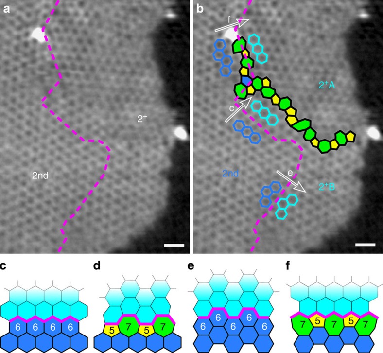
The existence of pentagon–heptagon pairs between the 2nd and the 2+ areas causes such rotation (30°) and can be clearly seen in Fig. 4. Figure 4a is a filtered image of Fig. 2d in which only the C atoms in layer 2 are shown (reflections corresponding to atoms in the 1st layer were deleted from a Fourier transform of Fig. 2d, and an inverse Fourier transform of the remaining spots gives the contrast of the C atoms in layer 2). The dashed magenta line separates the pristine area in the 2nd layer (left-hand side) from the new growth in the 2+ areas (right-hand side). The atomic growth processes can be identified from the image in Fig. 4b. The growth mechanisms can be classified into four categories: (i) from ZZ to ZZ (Fig. 4c), (ii) from reconstructed ZZ (57) to AC (Fig. 4d), (iii) from AC to AC (Fig. 4e) and (iv) from reconstructed AC (57) to ZZ (Fig. 4f). The step-edges in the original area (magenta lines in Fig. 4c–f) act as seeds for the new growth. The three growth mechanisms (i), (iii) and (iv) are found in Fig. 4b. The new growth area can be divided into two domains: 2+A and 2+B. The 2+B domain, which has the same orientation as the original 2nd layer, is an area grown from ZZ and AC edges, while the 2+A domain, which is rotated by 30° with respect to the original 2nd layer, is grown from a reconstructed AC (57) edge. At the boundary of the two domains, pentagon–heptagon pairs appear, as shown in Fig. 4b. The formation of such a grain boundary is similar to that formed in polycrystalline graphene synthesized by CVD.
Figure 4. Growth model determined by step-edge structure.
(a) A filtered image of Fig. 2d only showing the 2nd and 2+-layer graphene. The dashed magenta lines indicate the edge of initial 2nd layer. (b) Identical image to a with highlighted 5–7 defect structure (yellow pentagon and green heptagon). Blue hexagons stand for the initial 2nd-layer structure, from where the 2+ layer (cyan hexagons) grows along the white arrows. (c–f) Four categories of the growth model. (c) From ZZ to ZZ, (d) from reconstructed ZZ (57) to AC, (e) from AC to AC and (f) from reconstructed AC (57) to ZZ. Scale bar, 0.5 nm.
The same phenomenon of 30° rotating growth from the AB stacking bilayer graphene edge is shown in Supplementary Fig. 3. The new growth 2+ area indicated by the cyan rectangle has a different moiré pattern from that of the original 2nd layer. By applying the same method used for Fig. 4a, we again found that the zigzag chains of the 2+ and 2nd-layer areas had a rotation angle of about 30°. ADF images of bilayer graphene with a nearly 30° twisting angle between layers 1 and 2 are shown in Supplementary Fig. 4, and those images also show that there is an almost 30° rotation of the zigzag chains between the 2+ and original 2nd-layer areas. This 30° rotation is due to the 5–7 pairs on the 2nd-layer edge before growth. These 5–7-pair-terminated edges can be found in monolayer graphene or some bilayer graphene as shown in Supplementary Fig. 5. Zigzag edges are metastable20, and a planar reconstruction of the zigzag edge into the recently reported ZZ (57) edge structure was noted by Koskinen et al.20 to lead to a lower edge energy and a self-passivating edge that would not bond with hydrogen atoms. This is the first time that the 5–7 structure has been found on the edge of the 2nd layer of bilayer graphene, from which new growth is rotated by 30° with respect to the original layer. Although AB stacking is the most preferable stacking sequence in graphite, in the case of few-layer (at least two) graphene, it would seem that the growth is determined by the edge structure, as shown in Fig. 4c–f.
Such growth is only found in the 2nd layer (the 1st layer is a suspended layer), which means that a substrate is necessary for in-plane graphene growth. Another interesting result is that the two open edges of the 1st and 2nd layers will form a closed edge structure once the separation between the two is below a critical distance. This can be seen in Supplementary Fig. 6 and Supplementary Movie 4.
Step-edge graphene growth rates
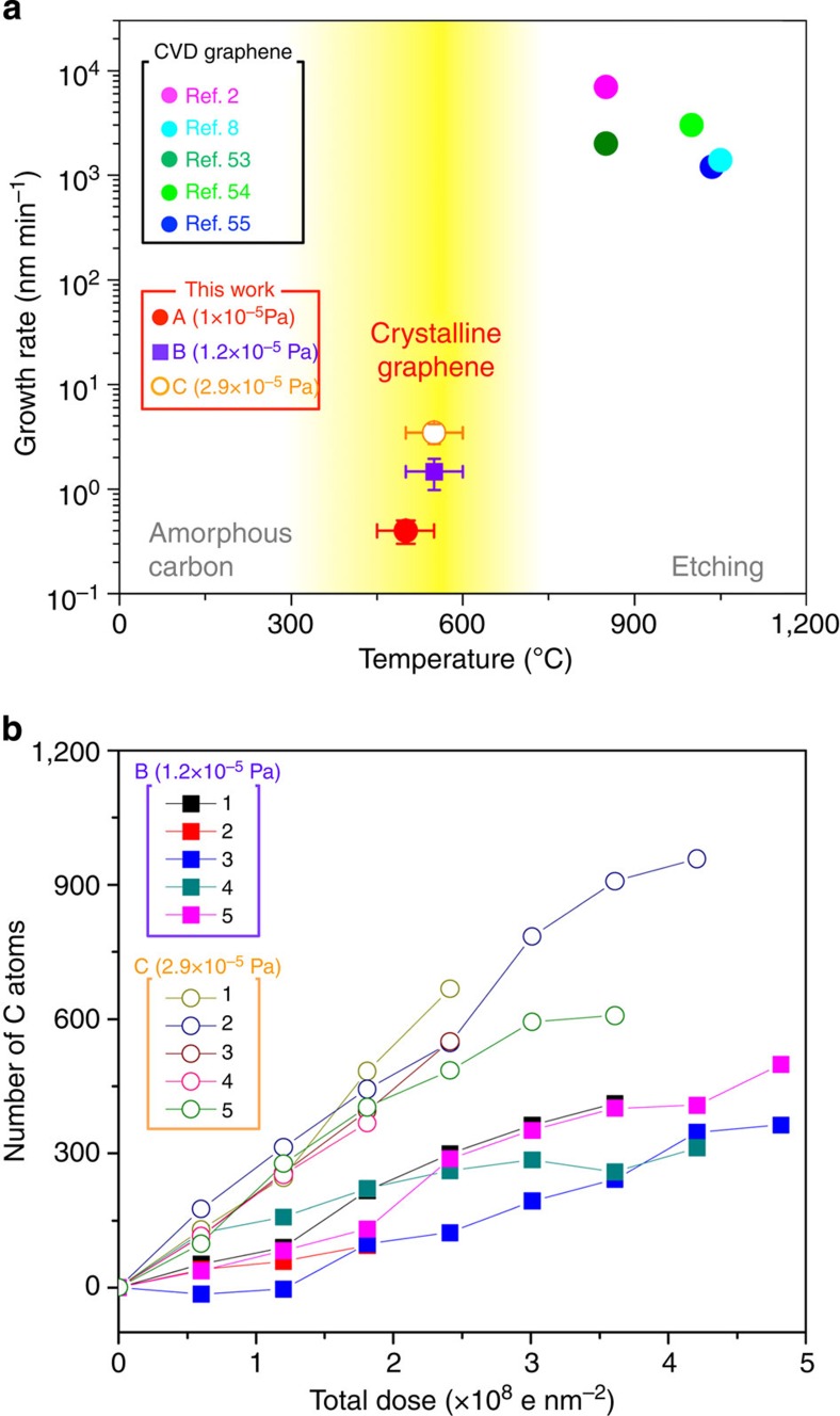
We can obtain a rough estimate of the growth rate by measuring the change in the size of the growth areas from series of sequential ADF images. The number of additional C atoms can be determined by counting the bright spots that represent C atoms in the ADF images or deduced from the increase in the size of the area; these two methods are equivalent within their respective errors. Figure 5a shows the temperature range in which the crystalline graphene grows in our study (500 °C<T<700 °C). At T<500 °C, the graphene does not grow in a crystalline structure but only amorphous carbon agglomerations are found on the first and second layer. On the other hand, the graphene edge is being etched during the observation at T>700 °C. This growth condition of graphene under the electron beam is different from the typical CVD conditions. To perceive the growth rate dependence of the residual hydrocarbon gas pressure, we have attempted experiments with different vacuum conditions. Figure 5b shows the growth rates at three different residual hydrocarbon gas pressures. The pressure range is limited to 1.0–2.9 × 10⁻⁵ Pa for keeping the TEM workable condition. The growth rate seems to be affected by the residual gas pressure. There is a tendency that if there are more residual hydrocarbon gases left in the TEM chamber, the growth rate will be faster.
Figure 5. Step-edge growth rate.
(a) Comparison between high-speed growth (CVD) and low-speed growth in this study. In this study, between 500 and 700 °C, graphene grows from step-edge. Three different growth rates at different residual hydrocarbon gas pressures are shown. The growth rates at 2.9 × 10⁻⁵ Pa are shown by circles and the growth rates at 1.2 × 10⁻⁵ Pa are shown by rectangles. When T<500 °C, amorphous carbons appear as contaminations. If T>700 °C, carbon atoms at step-edges are etched and no more graphene growth is found. (b) The growth speed measurements on different selected areas repeated five times at each residual hydrocarbon gas pressure for 1.2 × 10⁻⁵ and 2.9 × 10⁻⁵ Pa.
We know that the step-edge in-plane growth seen here is not just simple physical absorption of C atoms because single Si catalyst atoms are present at the bilayer edges. The electron beam also plays an important role in the growth by accumulating hydrocarbon gas at the scanned area; there is no growth in areas far from the scanned area as shown in Supplementary Fig. 7. It is well known that graphene growth is strongly dependent on the number of available C atoms that are able to bond within a certain time, that is, if a large number of C atoms encounter graphene edges and do not have enough time to locate an energetically optimal location before forming covalent bonds, then the graphene will just be contaminated with amorphous C. This is the case when graphene is observed in the STEM at RT and low-vacuum conditions. However, if the substrate graphene is heated to 500–700 °C, then the incident C atoms are more likely to form sp2 bonds with the step-edge atoms, and in-plane graphene growth will occur. At temperatures above 700 °C, the etching effect is dominant, and no growth was observed (Fig. 5). As shown in Fig. 5, the growth rates found in this study were very low (several angstroms per minute) in comparison with that of CVD20 (several micrometres per minute). Even though the vacuum conditions and gas source pressure were different from those in CVD, we were still able to successfully induce graphene growth and observe the growth at atomic resolutions.
Such in situ growth could be used to precisely design the orientation of graphene or other heterobilayer materials. When the pristine seed edges are terminated with ZZ or AC edges, the orientation of new growth area will remain the same; when the seed edges are terminated with some 5–7 defects, the new growth area will rotate by 30° with respect to the original layer. If the seed edges can be modified to terminate with other kinds of defects, rotation angle between 0° and 30° will be achieved. Since the growth speeds are dependent on the residual hydrocarbon gas pressures, observations by using environmental electron microscope with controlled carbon source are expected to offer more important information and attract attention to techniques controlling the growth of graphene or similar heterobilayer materials.
Methods
Graphene synthesis and transfer
SC-BLG were grown by the ambient pressure CVD of methane (99.99%) on polycrystalline Cu foil. Before growth, the Cu foil was soaked in acetic acid for 30 min to remove the surface oxides. The Cu foil was then mounted in the CVD chamber and the furnace was ramped up to 1,050 °C over 40 min, with constant flow of Ar (300 s.c.c.m.) and H2 (10 s.c.c.m.). After reaching 1,050 °C, the sample was annealed for 90 min without changing the gas flow. For graphene growth, methane (80 p.p.m.) was mixed with the flows of Ar (300 s.c.c.m.) and H2 (15 s.c.c.m.). H2 was fed into the reaction chamber for ~7 min to form bilayer graphene. After the growth, the Cu foil was moved to the cooling zone.
For the transfer process, the as-grown graphene sheet on Cu foil was first spin coated with a layer of polycarbonate, followed by etching in HCl aqueous solution to remove the Cu foil. The polycarbonate film and the attached graphene flakes were then transferred onto a Mo-quantifoil grid for TEM observations. EDS analyses demonstrate that there is no Cu left.
STEM and EELS observations
ADF imaging and EELS analysis were performed on a JEOL 2100F with a cold field-emission gun and an aberration corrector (the DELTA-corrector) operating at 60 kV. A Gatan GIF Quantum was used for the EELS chemical analyses. Typically, a 0.11-nm resolution was achieved for the STEM ADF imaging. The inner and outer collection angles for the ADF image (β1 and β2) were 58 and 129–140 mrad, respectively. The beam current was about 15 pA for the ADF imaging and EELS chemical analyses. The images shown in this paper are taken at high temperature (from 500 to 650 °C), while the experiments have been performed at a wider range of temperatures (from 300 to 1,000 K). Scan rate is 38 μs per pixel for faster scan and 58 μs for atomic resolution image. The images are filtered by a commercial software named HREM-Filters Pro. Vacuum conditions for different residual gas pressures were obtained by switching the trap pump on/off and by controlling the evacuation time.
Author contributions
C.-C.L., C.-H.Y. and P.-W.C. synthesized the materials. Z.L. and Y.-C.L. performed the experiments. Z.L. and Y.-C.L. analysed the data. Z.L., Y.-C.L., S.I. and K.S. co-wrote the paper. All authors discussed the results and commented on the manuscript.
Additional information
How to cite this article: Liu, Z. et al. In situ observation of step-edge in-plane growth of graphene in a STEM. Nat. Commun. 5:4055 doi: 10.1038/ncomms5055 (2014).
Supplementary Material
Supplementary Figures 1-7
Movie showing Si atoms act as catalysts during graphene growth from BLG step-edge. Higher frame rate employed here allows us to monitor the Si atom positions at a cost of SN ratio for graphene lattice contrast. The images are taken at 650°C. The movie plays 20 times faster than the real time.
Movie showing Si atoms act as catalysts during graphene growth from BLG step-edge. Higher frame rate employed here allows us to monitor the Si atom positions at a cost of SN ratio for graphene lattice contrast. The images are taken at 650°C. The movie plays 17 times faster than the real time.
Movie showing Si atoms act as catalysts during graphene growth from BLG step-edge. Higher frame rate employed here allows us to monitor the Si atom positions at a cost of SN ratio for graphene lattice contrast. The images are taken at 650°C. The movie plays 18 times faster than the real time.
Two open edges of 1st and 2nd layers connect together and leave the edge into a closed structure. The images are taken at 500°C. The movie plays 32 times faster than the real time.
Acknowledgments
This work is supported by Grant-in-Aid for Scientific Research on Innovative Areas (MEXT KAKENHI Grant Number 25107003). Z.L., Y.-C.L. and K.S. acknowledge support from a JST Research Acceleration Program. P.-W.C. acknowledges project support from Taiwan Ministry of Science and Technology (NSC 100-2112-M-007-014-MY3).
References
- Novoselov K. S. et al. Electric field effect in atomically thin carbon films. Science 30, 666–669 (2004). [DOI] [PubMed] [Google Scholar]
- Sutter P. W., Flege J.-I. & Sutter E. A. Epitaxial graphene on ruthenium. Nat. Mater. 7, 406–411 (2008). [DOI] [PubMed] [Google Scholar]
- Kim K. S. et al. Large-scale pattern growth of graphene films for stretchable transparent electrodes. Nature 457, 706–710 (2009). [DOI] [PubMed] [Google Scholar]
- Reina A. et al. Large area, few-layer graphene films on arbitrary substrates by chemical vapor deposition. Nano Lett. 9, 30–35 (2009). [DOI] [PubMed] [Google Scholar]
- Li X. et al. Large-area synthesis of high-quality and uniform graphene films on copper foils. Science 324, 1312–1314 (2009). [DOI] [PubMed] [Google Scholar]
- Lu C.-C. et al. Characterization of graphene grown on bulk and thin film nickel. Langmuir 27, 13748–13753 (2011). [DOI] [PubMed] [Google Scholar]
- Robertson A. W. & Warner J. H. Hexagonal single crystal domains of few-layer graphene on copper foils. Nano Lett. 11, 1182–1189 (2011). [DOI] [PubMed] [Google Scholar]
- Lu C.-C. et al. Twisting bilayer graphene superlattices. ACS Nano 7, 2587–2594 (2013). [DOI] [PubMed] [Google Scholar]
- Eda G., Fanchini G. & Chhowalla M. Large-area ultrathin films of reduced graphene oxide as a transparent and flexible electronic material. Nat. Nanotechnol. 3, 270–274 (2008). [DOI] [PubMed] [Google Scholar]
- Berger C. et al. Electronic confinement and coherence in patterned epitaxial graphene. Science 312, 1191–1196 (2006). [DOI] [PubMed] [Google Scholar]
- Emtsev K. V. et al. Towards wafer-size graphene layers by atmospheric pressure graphitization of silicon carbide. Nat. Mater. 8, 203–207 (2009). [DOI] [PubMed] [Google Scholar]
- Park J. et al. Epitaxial graphene growth by carbon molecular beam epitaxy (CMBE). Adv. Mater. 22, 4140–4145 (2010). [DOI] [PubMed] [Google Scholar]
- Maeda F. & Hibino H. Molecular beam epitaxial growth of graphene using cracked ethylene -advantage over ethanol in growth. Diamond Relat. Mater. 34, 84–88 (2013). [Google Scholar]
- Maeda F. & Hibino H. Growth of few-layer graphene by gas-source molecular beam epitaxy using cracked ethanol. Phys. Status Solidi B 247, 916–920 (2010). [Google Scholar]
- Seitsonen A. P., Saitta A. M., Wassmann T., Lazzeri M. & Mauri F. Structure and stability of graphene nanoribbons in oxygen, carbon dioxide, water, and ammonia. Phys. Rev. B 82, 115425 (2010). [Google Scholar]
- Ritter K. A. & Lyding J. W. The influence of edge structure on the electronic properties of graphene quantum dots and nanoribbons. Nat. Mater. 8, 235–242 (2009). [DOI] [PubMed] [Google Scholar]
- Singh A. K. & Yakobson B. I. Electronics and magnetism of patterned graphene nanoroads. Nano Lett. 9, 1540–1543 (2009). [DOI] [PubMed] [Google Scholar]
- Bhowmick S. & Shenoy V. B. Edge state magnetism of single layer graphene nanostructures. J. Chem. Phys. 128, 244717 (2008). [DOI] [PubMed] [Google Scholar]
- Ponomarenko L. A. et al. Chaotic Dirac billiard in graphene quantum dots. Science 320, 356–358 (2008). [DOI] [PubMed] [Google Scholar]
- Koskinen P., Malola S. & Häkkinen H. Self-passivating edge reconstructions of graphene. Phys. Rev. Lett. 101, 115502 (2008). [DOI] [PubMed] [Google Scholar]
- Yang L., Park C.-H., Son Y.-W., Cohen M. L. & Louie S. G. Quasiparticle energies and band gaps in graphene nanoribbons. Phys. Rev. Lett. 99, 186801 (2007). [DOI] [PubMed] [Google Scholar]
- Barone V., Hod O. & Scuseria G. E. Electronic structure and stability of semiconducting graphene nanoribbons. Nano Lett. 6, 2748–2754 (2006). [DOI] [PubMed] [Google Scholar]
- Son Y.-W., Cohen M. L. & Louie S. G. Energy gaps in graphene nanoribbons. Phys. Rev. Lett. 97, 216803 (2006). [DOI] [PubMed] [Google Scholar]
- Son Y.-W., Cohen M. L. & Louie S. G. Half-metallic graphene nanoribbons. Nature 444, 347–349 (2006). [DOI] [PubMed] [Google Scholar]
- Nakada K., Fujita M., Dresselhaus G. & Dresselhaus M. S. Edge state in graphene ribbons: nanometer size effect and edge shape dependence. Phys. Rev. B 54, 17954–17961 (1996). [DOI] [PubMed] [Google Scholar]
- Niimi Y. et al. Scanning tunneling microscopy and spectroscopy of the electronic local density of states of graphite surfaces near monoatomic step-edges. Phys. Rev. B 73, 085421 (2006). [Google Scholar]
- Kobayashi Y., Fukui K., Enoki T., Kusakabe K. & Kaburagi Y. Observation of zigzag and armchair edges of graphite using scanning tunneling microscopy and spectroscopy. Phys. Rev. B 71, 193406 (2005). [Google Scholar]
- Koskinen P., Malola S. & Häkkinen H. Evidence for graphene edges beyond zigzag and armchair. Phys. Rev. B 80, 073401 (2009). [Google Scholar]
- Seitsonen A. P. Structure and stability of graphene nanoribbons in oxygen, carbon dioxide, water, and ammonia. Phys. Rev. B 82, 115425 (2010). [Google Scholar]
- Kroes J. M. H., Akhukov M. A., Los J. H., Pineau N. & Fasolino A. Mechanism and free-energy barrier of the type-57 reconstruction of the zigzag edge of graphene. Phys. Rev. B 83, 165411 (2011). [Google Scholar]
- Wassmann T., Seitsonen A. P., Saitta A. M., Lazzeri M. & Mauri F. Structure, stability, edge states, and aromaticity of graphene ribbons. Phys. Rev. Lett. 101, 096402 (2008). [DOI] [PubMed] [Google Scholar]
- Kotakoski J., Santos-Cottin D. & Krasheninnikov A. V. Stability of graphene edges under electron beam: equilibrium energetics versus dynamic effects. ACS Nano 6, 671–676 (2012). [DOI] [PubMed] [Google Scholar]
- Kim K. et al. Atomically perfect torn graphene edges and their reversible reconstruction. Nat. Commun. 4, 2723 (2013). [DOI] [PubMed] [Google Scholar]
- Li X.-F., Wang L.-L., Chen K.-Q. & Luo Y. Electronic transport through zigzag/armchair graphene nanoribbon heterojunctions. J. Phys. Condens. Matter 24, 095801 (2012). [DOI] [PubMed] [Google Scholar]
- Li T. C. & Lu S.-P. Quantum conductance of graphene nanoribbons with edge defects. Phys. Rev. B 77, 085408 (2008). [Google Scholar]
- Sutter P. & Sutter E. Microscopy of graphene growth, processing, and properties. Adv. Mater. 23, 2617–2634 (2013). [Google Scholar]
- Man K. L. & Altman M. S. Low energy electron microscopy and photoemission electron microscopy investigation of graphene. J. Phys. Condens. Matter 24, 314209 (2012). [DOI] [PubMed] [Google Scholar]
- Ishigami M., Chen J. H., Cullen W. G., Fuhrer M. S. & Williams E. D. Atomic structure of graphene on SiO2. Nano Lett. 7, 1643–1648 (2007). [DOI] [PubMed] [Google Scholar]
- Coraux J., N′Diaye A. T., Busse C. & Michely T. Structural coherency of graphene on Ir(111). Nano Lett. 8, 565–570 (2008). [DOI] [PubMed] [Google Scholar]
- Meyer J. C. et al. The structure of suspended graphene sheets. Nature 446, 60–63 (2007). [DOI] [PubMed] [Google Scholar]
- Girit Ç. Ö. et al. Graphene at the edge: stability and dynamics. Science 323, 1705–1708 (2009). [DOI] [PubMed] [Google Scholar]
- Meyer J. C. et al. Direct imaging of lattice atoms and topological defects in graphene membranes. Nano Lett. 8, 3582–3586 (2008). [DOI] [PubMed] [Google Scholar]
- Gass M. H. et al. Free-standing graphene at atomic resolution. Nat. Nanotechnol. 3, 676–681 (2008). [DOI] [PubMed] [Google Scholar]
- Liu Z., Suenaga K., Harris P. J. F. & Iijima S. Open and closed edges of graphene layers. Phys. Rev. Lett. 102, 015501 (2009). [DOI] [PubMed] [Google Scholar]
- Warner J. H. et al. Structural transformations in graphene studied with high spatial and temporal resolution. Nat. Nanotechnol. 4, 500–504 (2009). [DOI] [PubMed] [Google Scholar]
- Xie L. et al. Graphene nanoribbons from unzipped carbon nanotubes: atomic structures, Raman spectroscopy and electrical properties. J. Am. Chem. Soc. 113, 10394–10397 (2011). [DOI] [PubMed] [Google Scholar]
- Kotakoski J., Krasheninnikov A. V., Kaiser U. & Meyer J. C. From point defects in graphene to two-dimensional amorphous carbon. Phys. Rev. Lett. 106, 105505 (2011). [DOI] [PubMed] [Google Scholar]
- Song B. et al. Atomic-scale electron-beam sculpting of near-defect-free graphene nanostructures. Nano Lett. 11, 2247–2250 (2011). [DOI] [PubMed] [Google Scholar]
- Jin C., Lan H., Peng L., Suenaga K. & Iijima S. Deriving carbon atomic chains from graphene. Phys. Rev. Lett. 102, 205501 (2009). [DOI] [PubMed] [Google Scholar]
- Chuvilin A., Meyer J. C., Algara-Siller G. & Kaiser U. From graphene constrictions to single carbon chains. New J. Phys. 11, 083019 (2009). [Google Scholar]
- Dimiev A. et al. Layer-by-layer removal of graphene for device patterning. Science 331, 1168–1172 (2011). [DOI] [PubMed] [Google Scholar]
- Zan R., Ramasse Q. M., Bangert U. & Novoselov K. S. Graphene reknits its holes. Nano Lett. 12, 3936–3940 (2012). [DOI] [PubMed] [Google Scholar]
- Lu C.-C. et al. Twisting bilayer graphene superlattices. Nano Lett. 7, 2587–2594 (2013). [DOI] [PubMed] [Google Scholar]
- Li X., Cai W., Colombo L. & Ruoff R. S. Evolution of graphene growth on Ni and Cu by carbon isotope labeling. Nano Lett. 9, 4268–4272 (2009). [DOI] [PubMed] [Google Scholar]
- Li X. et al. Large-area graphene single crystals grown by low-pressure chemical vapor deposition of methane on copper. J. Am. Chem. Soc. 133, 2816–2819 (2011). [DOI] [PubMed] [Google Scholar]
Associated Data
This section collects any data citations, data availability statements, or supplementary materials included in this article.
Supplementary Materials
Supplementary Figures 1-7
Movie showing Si atoms act as catalysts during graphene growth from BLG step-edge. Higher frame rate employed here allows us to monitor the Si atom positions at a cost of SN ratio for graphene lattice contrast. The images are taken at 650°C. The movie plays 20 times faster than the real time.
Movie showing Si atoms act as catalysts during graphene growth from BLG step-edge. Higher frame rate employed here allows us to monitor the Si atom positions at a cost of SN ratio for graphene lattice contrast. The images are taken at 650°C. The movie plays 17 times faster than the real time.
Movie showing Si atoms act as catalysts during graphene growth from BLG step-edge. Higher frame rate employed here allows us to monitor the Si atom positions at a cost of SN ratio for graphene lattice contrast. The images are taken at 650°C. The movie plays 18 times faster than the real time.
Two open edges of 1st and 2nd layers connect together and leave the edge into a closed structure. The images are taken at 500°C. The movie plays 32 times faster than the real time.


